Package Assembly Including Lid with Additional Stress Mitigating Feet and Methods of Making the Same
Abstract
A package assembly includes a package substrate, a package lid located on the package substrate and including a plate portion, an outer foot extending from the plate portion, and an inner foot having a height greater than or equal to a height of the outer foot, extending from the plate portion and including a first inner foot corner portion located inside a first corner of the outer foot, and an adhesive that adheres the outer foot to the package substrate and adheres the inner foot to the package substrate.
Claims (20)
1. A package assembly comprising: a package substrate; a package lid on the package substrate, comprising: a plate portion; an outer foot extending from the plate portion; and an inner foot having a height greater than or equal to a height of the outer foot, extending from the plate portion and including a first inner foot corner portion located inside a first corner of the outer foot; and an adhesive that adheres the outer foot to the package substrate and adheres the inner foot to the package substrate.
16. A method of making a package assembly, the method comprising: forming an adhesive on a package substrate; placing a package lid on the adhesive, the package lid comprising: a plate portion; an outer foot extending from the plate portion; and an inner foot having a height greater than or equal to a height of the outer foot, extending from the plate portion and including a first inner foot corner portion located inside a first corner of the outer foot; and pressing the package lid onto the package substrate and curing the adhesive so that the adhesive adheres the outer foot to the package substrate and the inner foot to the package substrate.
20. A package assembly comprising: a package substrate; a molded die module on the package substrate, wherein the molded die module comprises a plurality of semiconductor dies separated by a molding gap extending lengthwise in a first direction; a secondary die on the package substrate adjacent to the molded die module; and a package lid comprising: a ring portion around the molded die module on the package substrate; and a plate portion on the ring portion and over the molded die module and secondary die, and including: a first cavity that is located at an edge of the molded die module; and a second cavity extending lengthwise in the first direction and substantially aligned with the molding gap.
Show 17 dependent claims
2. The package assembly of claim 1 , wherein the height of the inner foot is substantially equal to the height of the outer foot.
3. The package assembly of claim 1 , wherein the height of the inner foot is greater than the height of the outer foot.
4. The package assembly of claim 3 , wherein the package substrate comprises a recessed portion and the inner foot is adhered to the package substrate inside the recessed portion.
5. The package assembly of claim 4 , wherein the package substrate comprises a core substrate and an upper insulating layer on the core substrate, and the recessed portion is formed in the upper insulating layer.
6. The package assembly of claim 5 , wherein the inner foot is adhered inside the recessed portion to the upper insulating layer.
7. The package assembly of claim 5 , wherein the inner foot is adhered inside the recessed portion to the core substrate.
8. The package assembly of claim 1 , wherein the outer foot comprises a first outer foot side and a second outer foot side, and the first inner foot corner portion comprises a first inner foot corner portion side extending along the first outer foot side and having a length L b1 that is less than a length L ax of the first outer foot side.
9. The package assembly of claim 8 , wherein the first inner foot corner portion further comprises a second inner foot corner portion side extending along the second outer foot side and having a length L b1 that is less than a length L ay of the second outer foot side.
10. The package assembly of claim 9 , wherein L b1 ≥0.1×L ax and L b1 ≥0.1×L ay .
11. The package assembly of claim 1 , wherein the inner foot further comprises a second inner foot corner portion located inside a second corner of the outer foot, and the second inner foot corner portion is separate from the first inner foot corner portion.
12. The package assembly of claim 11 , wherein the inner foot further comprises a first inner foot line portion between the first inner foot corner portion and the second inner foot corner portion.
13. The package assembly of claim 1 , wherein a thickness of the inner foot is greater than a thickness of the outer foot.
14. The package assembly of claim 1 , wherein a distance between the inner foot and the outer foot is greater than 500 μm.
15. The package assembly of claim 1 , further comprising: an interposer module mounted on the package substrate under the plate portion of the package lid; and a thermal interface material (TIM) film on the interposer module and between the interposer module and the plate portion of the package lid, wherein a distance between the inner foot and the TIM film is greater than 1000 μm.
17. The method of claim 16 , further comprising: forming a recessed portion in the package substrate, wherein the forming of the adhesive comprises forming the adhesive in the recessed portion and the placing of the package lid on the adhesive comprises placing the inner foot inside the recessed portion.
18. The method of claim 17 , wherein the package substrate comprises a core substrate and an upper insulating layer on the core substrate, and the forming of the recessed portion comprises forming the recessed portion in the upper insulating layer.
19. The method of claim 18 , wherein the placing of the inner foot inside the recessed portion comprises placing the inner foot on the core substrate inside the recessed portion.
Full Description
Show full text →
RELATED APPLICATIONS
This application claims the benefit of priority from U.S. Provisional Application No. 63/222,234, entitled “TIM1 Stress Mitigation Method by Reinforce Embedded Lid Foot Design” filed on Jul. 15, 2021, the entire contents of which are incorporated herein by reference for all purposes.
BACKGROUND
A package assembly may include one or more semiconductor devices (e.g., semiconductor dies, interposer modules, etc.) that may be mounted on a substrate. The package assembly may also include a package lid mounted on the substrate over the semiconductor devices. The package lid may include a foot that may be attached to the substrate by using an adhesive. A thermal interface material (TIM) film may be located between the semiconductor devices and the package lid. Designing the package assembly to avoid cracking and delamination of the TIM film may be challenging.
BRIEF DESCRIPTION OF THE DRAWINGS
Aspects of the present disclosure are best understood from the following detailed description when read with the accompanying figures. It is noted that, in accordance with the standard practice in the industry, various features are not drawn to scale. In fact, the dimensions of the various features may be arbitrarily increased or reduced for clarity of discussion.
A is a vertical cross-sectional view of a package assembly (e.g., organic/silicon interposer package) according to one or more embodiments.
B is a perspective view of a package lid that may be included in the package assembly according to one or more embodiments.
C is a plan view of the bottom surface of the plate portion of the package lid according to one or more embodiments.
D is a vertical cross-sectional view of a package assembly (e.g., organic/silicon interposer package) according to one or more embodiments.
E is a vertical cross-sectional view of a package assembly (e.g., organic/silicon interposer package) according to one or more embodiments.
A is a perspective view of a package lid that may be included in the package assembly according to one or more embodiments.
B is a plan view of the bottom surface of the plate portion of the package lid according to one or more embodiments.
A is a perspective view of a package lid that may be included in the package assembly according to one or more embodiments.
B is a plan view of the bottom surface of the plate portion of the package lid according to one or more embodiments.
A and 4 B illustrate a recessed portion for a package assembly according to one or more embodiments.
A illustrates a plan view of the inner foot on the upper insulating layer of a package substrate according to one or more embodiments.
B is a vertical cross-sectional view of the inner foot according to one or more embodiments.
A illustrates a perspective view of the inner foot according to one or more embodiments.
B is a vertical cross-sectional view of the inner foot according to one or more embodiments.
A illustrates a vertical cross-sectional view of an intermediate structure in which the recessed portion may be formed in the upper insulating layer of the package substrate according to one or more embodiments.
B illustrates a vertical cross-sectional view of an intermediate structure in which the interposer module may be mounted on the package substrate (e.g., via a flip chip bonding (FCB) process) according to one or more embodiments.
C illustrates a vertical cross-sectional view of an intermediate structure in which the package underfill layer may be formed on the package substrate according to one or more embodiments.
D illustrates a vertical cross-sectional view of an intermediate structure in which the TIM film may be formed on (e.g., dispensed on) or attached to the upper surface of the interposer module according to one or more embodiments.
E illustrates a vertical cross-sectional view of an intermediate structure in which the adhesive may be applied to the package substrate according to one or more embodiments.
F illustrates a vertical cross-sectional view of an intermediate structure in which the package lid may be attached to (e.g., mounted on) the package substrate according to one or more embodiments.
G illustrates a vertical cross-sectional view of an intermediate structure in which a plurality of solder balls may be formed on the package substrate according to one or more embodiments.
is a flow chart illustrating a method of making a package assembly according to one or more embodiments.
is a vertical cross-sectional view of a package assembly, according to one or more embodiments.
A is a plan view of a surface of the package substrate in the package assembly, according to one or more embodiments.
B is a plan view of the molded die module, according to one or more embodiments.
A is a perspective view of the plate portion of the package lid, according to one or more embodiments.
B is a plan view of the bottom surface of the plate portion, according to one or more embodiments.
A is a plan view of a surface of the package substrate in an alternative design of the package assembly, according to one or more embodiments.
B is a plan view of the bottom surface of the plate portion in the alternative design of the package assembly, according to one or more embodiments
A is a plan view of a surface of the package substrate in an alternative design of the package assembly, according to one or more embodiments.
B is a plan view of the bottom surface of the plate portion in the alternative design of the package assembly, according to one or more embodiments.
A is a plan view of a surface of the package substrate in an alternative design of the package assembly, according to one or more embodiments.
B is a plan view of the bottom surface of the plate portion in the alternative design of the package assembly, according to one or more embodiments.
is a flow chart illustrating a method of making a package assembly according to one or more embodiments.
A is a vertical cross-sectional view of a package assembly according to one or more embodiments.
B is a plan view of a surface of the package substrate in the package assembly, according to one or more embodiments.
C is a plan view of the bottom surface of the plate portion, according to one or more embodiments.
is a plan view of the bottom surface of the plate portion in a first alternative design of the package assembly, according to one or more embodiments.
is a plan view of the bottom surface of the plate portion in a second alternative design of the package assembly, according to one or more embodiments.
A is a plan view of the package substrate in a third alternative design of the package assembly, according to one or more embodiments
B is a plan view of the bottom surface of the plate portion in the third alternative design of the package assembly, according to one or more embodiments.
A is a plan view of the package substrate in a fourth alternative design of the package assembly, according to one or more embodiments.
B is a plan view of the bottom surface of the plate portion in the fourth alternative design of the package assembly, according to one or more embodiments.
A illustrates a package assembly according to one or more embodiments.
B is a plan view of the package substrate in the package assembly, according to one or more embodiments.
C is a vertical cross-sectional view of the package assembly, according to one or more embodiments.
D is a vertical cross-sectional view of the package assembly, according to one or more embodiments.
A is a plan view of the package substrate in a first alternative design of the package assembly, according to one or more embodiments.
B is a plan view of the package substrate in a second alternative design of the package assembly, according to one or more embodiments.
C is a plan view of the package substrate in a third alternative design of the package assembly, according to one or more embodiments.
D is a plan view of the package substrate in a fourth alternative design of the package assembly, according to one or more embodiments.
DETAILED DESCRIPTION
The following disclosure provides many different embodiments, or examples, for implementing different features of the provided subject matter. Specific examples of components and arrangements are described below to simplify the present disclosure. These are, of course, merely examples and are not intended to be limiting. For example, the formation of a first feature over or on a second feature in the description that follows may include embodiments in which the first and second features are formed in direct contact, and may also include embodiments in which additional features may be formed between the first and second features, such that the first and second features may not be in direct contact. In addition, the present disclosure may repeat reference numerals and/or letters in the various examples. This repetition is for the purpose of simplicity and clarity and does not in itself dictate a relationship between the various embodiments and/or configurations discussed.
Further, spatially relative terms, such as “beneath,” “below,” “lower,” “above,” “upper” and the like, may be used herein for ease of description to describe one element or feature's relationship to another element(s) or feature(s) as illustrated in the figures. The spatially relative terms are intended to encompass different orientations of the device in use or operation in addition to the orientation depicted in the figures. The apparatus may be otherwise oriented (rotated 90 degrees or at other orientations) and the spatially relative descriptors used herein may likewise be interpreted accordingly. Unless explicitly stated otherwise, each element having the same reference numeral is presumed to have the same material composition and to have a thickness within a same thickness range.
One or more embodiments may include a thermal interface material film (TIM film) (e.g., TIM1) stress mitigation method by reinforcement with an embedded lid foot design. For high-power integrated circuit production, a metal TIM film may be widely used in industry because of its high thermal conductivity performance. However, a metal TIM film has a potential increase in risk of cracking and delamination as the size is increased (e.g., larger than 10 mm×10 mm).
Typically, a package lid may include only one foot that may be referred to as an outer foot in a ring shape. In one or more embodiments, a package assembly may include a package lid having an outer foot and one or more inner feet. In particular, the package lid may include one or more embedded support feet that may be located in the corners of the package lid, respectively. The package assembly may also include a novel substrate shape to accommodate the lid feet embedded design, and novel adhesive pattern to accommodate the lid feet embedded design.
The embodiments may include several novel and inventive features including, for example, 1) a package lid including a corner-shaped inner foot that may be embedded in the package substrate (e.g., extra support embedded package lid), 2) a number of the inner feet that may be embedded (e.g., multi-embedded support package lids) may be greater than or equal to one, and 3) the package lid (e.g., the package lid with extra support) may avoid touching the passive components (e.g., resisters, capacitors, transformers, etc.).
One or more embodiments may have several advantages and benefits. A stress on the TIM film (e.g., TIM1 stress) may be mitigated so that a metal TIM film (e.g., a solder TIM) may not be restricted to only small chip-on-wafer (CoW) dies. The package lid (e.g., reinforced package lid foot structure) may also mitigate the stress-induced TIM crack and TIM delamination issue and, therefore, improve the reliability of a package assembly.
The package assembly may include a substrate and an interposer module on the substrate. The interposer module may include an organic interposer, a system on chip (SOC) device and high-bandwidth memory (HBM) connected to the organic interposer by a plurality of microbumps, a first underfill formed around the plurality of microbumps, and a molding material formed on the SOC device and HBM device. The package assembly may also include a TIM film on the interposer module, a plurality of C 4 bumps for connecting the interposer module to the substrate, a second underfill between the interposer module and substrate, a package lid attached to the substrate over the interposer module, and an adhesive for attaching the package lid to the substrate.
The package lid may include an outer foot having a first height and an inner foot having a second height. The second height may be greater than or equal to the first height. An embedded length of the inner foot may be equal to the difference between the second height and the first height.
On a first side of the package lid, the inner foot may extend over a first distance, and the outer foot may extend over a second distance, and the first distance may be greater than or equal to 10% of the second distance. On a second side of the package assembly that adjoins the first side, the inner foot may also extend over the first distance and the outer foot may extend over the second distance. The package lid may include a standard type in which an inner foot may be formed at a corner of the package lid, a multiple inner feet type (enhanced type-1) in which the inner foot includes line portions formed along a side of the package lid, and a heavy feet type (enhanced type-2) which may be similar to the multiple inner feet type, except that a thickness of the inner foot may be increased.
A length of an embedded portion of the inner foot may be variable. In particular, a package substrate may include a core substrate and an upper insulating layer formed on the core substrate. A difference between the height of the outer foot and the height of the inner foot may be zero (e.g., the height of the inner foot may be equal to the height of the outer foot). The length of the embedded portion of the inner foot may be greater than zero but less than the thickness of the upper insulating layer. That is, a length of the embedded portion of the inner foot (e.g., the supported embedded ring) may be anywhere between zero and the thickness of the upper insulating layer. If the length of the embedded portion exceeds the thickness of the upper insulating layer, it may result in other extra adverse effect on molding and underfill.
The inner foot (e.g., embedded inner foot) may act as a TIM stress reliever. That is, the embedded inner foot may improve the stress mitigation on the TIM film (e.g., TIM1). In particular, the stress on the TIM film with the new designed package lid can be about 15% less than a stress on the TIM film in a conventional package assembly. That is, for example, the novel package lid of the embodiments may reduce the stress from TIM1 stress=1 in a conventional package assembly to TIM1 stress=0.85 in one or more embodiments.
A method of making the package assembly may include, for example, before performing an on-substrate (oS) process, using a laser drilling technique on the package substrate to obtain the defined shape on the package substrate (e.g., to make a hole in the package substrate). In particular, the method may include the steps of 1) providing a substrate, 2) performing a laser drilling process for making a hole to embed the inner foot, 3) flip chip bonding an interposer module onto the package substrate and applying the underfill between the interposer module and package substrate, and 4) attaching the inner foot and outer foot (i.e., attaching the ring) to the package substrate by using an adhesive. The inner foot adhesive used to adhere the inner foot to the package substrate can be, for example, an epoxy adhesive or silicone adhesive. The inner foot adhesive can be the same as or different from the outer foot adhesive.
The package lid may be composed, for example, of polymer, metal or ceramic. In one or more embodiments, Cu/CuS304/SUS430 may be used as a material for the package lid. The package lid may be mold-formed, punched or stamped to have the inner foot and outer foot, or a CNC milling tool may be used to fabricate the package lid including the inner foot and outer foot.
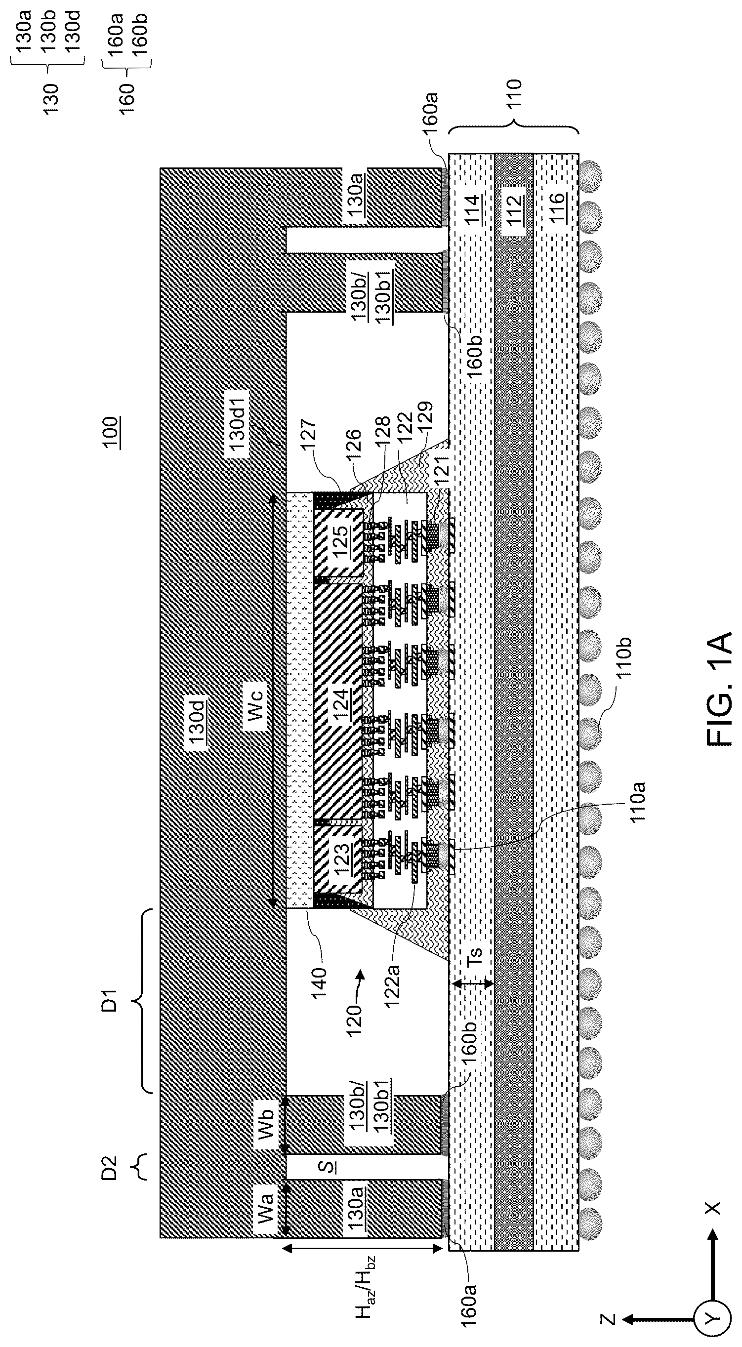
A is a vertical cross-sectional view of a package assembly 100 (e.g., organic/silicon interposer package) according to one or more embodiments. It should be noted that some background elements may be omitted from A for ease of explanation. B is a perspective view of a package lid 130 that may be included in the package assembly 100 according to one or more embodiments. C is a plan view of the bottom surface 130 d 1 of the plate portion 130 d of the package lid 130 according to one or more embodiments. The vertical cross-sectional view of the package assembly 100 in A is a view along the line I-I′ in the package lid 130 in C .
As illustrated in A , the package assembly 100 may include a package substrate 110 , an interposer module 120 mounted on the package substrate 110 , and a package lid 130 on the interposer module 120 and attached to the package substrate 110 . The package assembly 100 may also include a TIM film 140 formed on the interposer module 120 . The TIM film 140 may include, for example, a metal TIM film (e.g., a solder TIM), a thermal paste, thermal adhesive, thermal gap filler, thermal pad (e.g., silicone), thermal tape, a graphite TIM film, and a carbon nanotube TIM film. Other types of TIM films are within the contemplated scope of this disclosure.
The package substrate 110 may include any substrate that can support a package assembly including, for example, a system on integrated substrate (SoIS), a printed circuit board (PCB) etc. In one or more embodiments, the package substrate 110 may include a core substrate 112 (e.g., polymer substrate), an upper insulating layer 114 (e.g., chip-side insulating layer) having a thickness T s formed on the core substrate 112 , and a lower insulating layer 116 (e.g., board-side insulating layer) formed in contact with the core substrate 112 opposite the upper insulating layer 114 . The package substrate 110 may also include metal interconnects and through vias to provide an electrical connection of the package substrate 110 .
The package substrate 110 may also include metal bonding pads 110 a formed on a chip-side of the package substrate 110 , for providing an electrical connection to a semiconductor device (e.g., interposer module, semiconductor die, etc.) that is mounted on the package substrate 110 . A ball-grid array (BGA) including a plurality of solder balls 110 b may be formed on a board-side of the package substrate 110 that is opposite to the chip-side of the package substrate 110 . The solder balls 110 b may allow the package assembly 100 to be securely mounted on a substrate such as a printed circuit board (PCB) and electrically coupled to the substrate. The solder balls 110 b may be electrically connected to the metal bonding pads 110 a by the metal interconnects and through vias in the package substrate 110 .
The interposer module 120 may be mounted by C 4 bumps 121 on the metal bonding pads 110 a in the package substrate 110 . Although only one interposer module 120 is illustrated in A , the package assembly 120 may include more than one interposer module 120 . The interposer module 120 may include an interposer dielectric layer 122 that may embed metal interconnects 122 a connected to the C 4 bumps 121 . The interposer module 120 may also include a first semiconductor die 123 , second semiconductor die 124 and a third semiconductor die 125 that may all be mounted on the interposer dielectric layer 122 . While the embodiment illustrated in A includes a first semiconductor die 123 , second semiconductor die 124 and a third semiconductor die 125 , in other embodiments the interposer module 120 may include fewer or more semiconductor dies.
The first semiconductor die 123 , second semiconductor die 124 and third semiconductor die 125 may be mounted on the interposer dielectric layer 122 by micro-bumps 128 that may be electrically connected to the metal interconnects 122 a . A package underfill layer 129 may be formed under and around the interposer module 120 and the C 4 bumps 121 so as to adhere the interposer module 120 to the package substrate 110 . The package underfill layer 129 may be formed of an epoxy-based polymeric material.
Each of the first semiconductor die 123 , second semiconductor die 124 and third semiconductor die 125 may include, for example, a semiconductor die, a system on chip (SOC) die, a system on integrated chips (SoIC) die, and a high-bandwidth memory (HBM) die. In particular, the interposer module 120 may include a high-performance computing (HPC) application and may include, for example, an integrated graphics processing unit (GPU), application specific integrated circuit (ASIC), field-programmable gate array (FPGA), and HBM by chip on wafer on substrate (CoWoS) technology or integrated fan-out on substrate (INFO-oS) technology.
An interposer underfill layer 126 may be formed around the micro-bumps 128 and between the first semiconductor die 123 and the interposer dielectric layer 122 , between the second semiconductor die 124 and the interposer dielectric layer 122 , and between the third semiconductor die 125 and the interposer dielectric layer 122 . The interposer underfill layer 126 may be formed continuously as one layer under the first semiconductor die 123 , second semiconductor die 124 and third semiconductor die 125 , as illustrated in A . Alternatively, the interposer underfill layer 126 may be formed as three separate layers under the first semiconductor die 123 , second semiconductor die 124 and third semiconductor die 125 , respectively. The interposer underfill layer 126 may also be formed between first semiconductor die 123 and the second semiconductor die 124 , and between the second semiconductor die 124 and the third semiconductor die 125 . The interposer underfill layer 126 may also be formed of an epoxy-based polymeric material.
A molding material layer 127 may be formed over the first semiconductor die 123 , the second semiconductor die 124 , the third semiconductor die 125 , the interposer underfill layer 126 and the interposer dielectric layer 122 . The molding material layer 127 may be formed of an epoxy molding compound (EMC).
The TIM film 140 may be formed on the interposer module 120 to dissipate of heat generated during operation of the package assembly 100 (e.g., operation of first semiconductor die 123 , second semiconductor die 124 , and third semiconductor die). The TIM film 140 may include, for example, a metal TIM film that may be attached to the interposer module 120 , for example, by a thermally conductive adhesive. In particular, the TIM film 140 may contact an upper surface of first semiconductor die 123 , an upper surface of second semiconductor die 124 , an upper surface of the third semiconductor die 125 , and an upper surface of the molding material layer 127 . The TIM film 140 may have a low bulk thermal impedance and high thermal conductivity. The bond-line-thickness (BLT) (e.g., a distance between the package lid 130 and the interposer module 120 ) may be less than about 100 μm, although greater or lesser distances may be used.
The package assembly 100 may also include a stiffener ring (not shown) that may be adhered to the package substrate 110 by an adhesive (e.g., a silicone adhesive or an epoxy adhesive). The stiffener ring may be formed of a metal such as copper with a nickel coating, or an aluminum alloy. The stiffener ring may be formed on the package substrate 110 so as to surround the interposer module 120 . The stiffener ring may increase the rigidity to the package substrate 110 .
The package lid 130 may be on the TIM film 140 and may provide a cover for the interposer module 120 . The package lid 130 may contact at least a portion of the TIM film 140 . In one or more embodiments, the package lid 130 may directly contact an entire upper surface of the TIM film 140 . The package lid 130 may be formed, for example, of metal, ceramic or polymer material. The package lid 130 may include a plate portion 130 d that may cover the interposer module 120 . The plate portion 130 d may include a central region that is formed over a central portion of the interposer module 120 . A bottom surface 130 d 1 of the plate portion 130 d may extend across most of the plate portion 130 d and contact the TIM film 140 .
The package lid 130 may also include an outer foot 130 a and inner foot 130 b that may both extend from the plate portion 130 d (e.g., in the z direction in A ) and connect the package lid 130 to the package substrate 110 by an adhesive 160 . That is, the adhesive 160 may adhere the outer foot 130 a to the package substrate 110 and the inner foot 130 b to the package substrate 110 .
The inner foot 130 b may extend from the plate portion 130 d within a perimeter established by the outer foot 130 a . The inner foot 130 b may be separately formed from the outer foot 130 a . In particular, the inner foot 130 b may extend from the plate potion 130 d separately from the outer foot 130 a so that a space S may be formed between the inner foot 130 b and the outer foot 130 a . A distance D 1 (e.g., in the x-direction in A ) between the inner foot 130 b and the TIM film 140 (e.g., between the inner foot 130 b and the interposer module 120 ) may be greater than about 1000 μm. A distance D 2 between the inner foot 130 b and the outer foot 130 a (e.g., a width of the space S) may generally be in a range from about 0.2 mm to about 10 mm. In one or more embodiments, the distance D 2 may be in a range from about 0.5 mm (500 μm) to about 10 mm. A distance D 3 between the outer foot 130 a and the TIM film 140 (e.g., between the outer foot 130 a and the interposer module 120 ) may be greater than about 1500 μm. The distances D 1 , D 2 and D 3 may depend upon several factors such as a width (in the x-direction in A ) of the plate portion 130 d , a width Wb of the inner foot 130 b , a width Wa of the outer foot 130 a , a width We of the interposer module 120 (e.g., a width of the TIM film), etc.
The inner foot 130 b may have a width Wb that is greater than or equal to a width Wa of the outer foot 130 a . In particular, the outer foot 130 a may have a width Wa in a range from about 0.5 mm to about 6 mm, and the inner foot 130 b may have a width Wb in a range from about 1 mm to about 10 mm. The inner foot 130 b may have a height H bz from the bottom surface 130 d 1 of the plate portion 130 d that is substantially the same as a height H az of the outer foot 130 a . That is, the outer foot 130 a may extend from the plate portion 130 d by a first distance (i.e., H az ), and the inner foot 130 b may extend from the plate portion 130 d by a second distance (i.e., H bz ) substantially the same as the first distance. The inner foot 130 b may be formed on the package lid 130 , for example, by milling using a computer numerical control (CNC) milling machine, or by molding, punching or stamping the package lid 130 to include the inner foot 130 b.
The adhesive 160 may include, for example, epoxy adhesive or silicone adhesive. Other adhesives are within the contemplated scope of this disclosure. The adhesive 160 may include an adhesive outer portion 160 a that adheres the outer foot 130 a to the package substrate 110 , and an adhesive inner portion 160 b that adheres the inner foot 130 b to the package substrate 110 . The adhesive outer portion 160 a may be composed of the same adhesive material as the adhesive inner portion 160 b . Alternatively, the adhesive outer portion 160 a may be composed of an adhesive material that is different than that the adhesive inner portion 160 b . The adhesive outer portion 160 a may have a first thickness at the outer foot 130 a , and the adhesive inner portion 160 b may have a second thickness at the inner foot 130 b , and the second thickness may be substantially the same as than the first thickness.
The adhesive outer portion 160 a may have a shape (in a plan view) that corresponds to a shape of the outer foot 130 a , and the adhesive inner portion 160 b may have a shape (in a plan view) that corresponds to a shape of the inner foot 130 b . A width of the adhesive outer portion 160 a may be substantially the same as the width Wa of the outer foot 130 a , and a width of the adhesive inner portion 160 b may be substantially the same as the width Wb of the inner foot 130 b . That is, the adhesive outer portion 160 a may adhere to substantially all of the bottom surface of the outer foot 130 a , and the adhesive inner portion 160 b may adhere to substantially all of the bottom surface of the inner foot 130 b . In particular, an outermost edge and innermost edge of the adhesive outer portion 160 a may be substantially aligned with an outermost edge and innermost edge of the bottom of the outer foot 130 a , respectively, and an outermost edge and innermost edge of the adhesive inner portion 160 b may be substantially aligned with an outermost edge and innermost edge of the bottom of the inner foot 130 a , respectively.
As illustrated in B and 1 C , the package lid 130 may have a square shape or rectangle shape. Other suitable shapes of the package lid 130 may be within the contemplated scope of disclosure. The outer foot 130 a may be formed continuously around the entire perimeter of the bottom surface 130 d 1 of the plate portion 130 d . The inner foot 130 b may include one or more inner foot corner portions 130 b 1 having a corner shape or L-shape. The inner foot corner portions 130 b 1 may be located between the outer foot 130 a and the interposer module 120 in the x-direction and the y-direction in A . It should be noted that only the part of the inner foot corner portion 130 b 1 that extends in the y-direction is illustrated in the vertical cross-sectional view of A , and the lid is not limited thereto. The inner foot corner portion 130 b 1 may be formed inside each corner of the outer foot 130 a , and may be substantially aligned with the corresponding corner of the outer foot 130 a.
The bottom surface 130 d 1 of the plate portion 130 d may be bounded on all sides by the outer foot 130 a and may therefore, have a shape that corresponds to (e.g., is substantially the same as) the shape of the outer foot 130 a (i.e., a square shape as shown in C ). The outer foot 130 a may include a first outer foot side 130 ax and a second outer foot side 130 ay . The inner foot corner portion 130 b 1 may include a first inner foot corner portion side 130 b 1 x extending along the first outer foot side 130 ax . The first inner foot corner portion side 130 b 1 x may have a length L b1 that is less than a length L ax of the first outer foot side 130 ax . The inner foot corner portion 130 b 1 may also include a second inner foot corner portion side 130 b 1 y extending along the second outer foot side 130 ay . The second inner foot corner portion side 130 b 1 y may have a length L b1 that is less than a length L ay of the second outer foot side 130 ay . In particular, the length L b1 of the first inner foot corner portion side 130 b 1 x may be greater than or equal to 0.1 times the length L ax of the first outer foot side 130 ax . The length L b1 of the second inner foot corner portion side 130 b 1 y may be greater than or equal to 0.1 times the length L ay of the second outer foot side 130 ay.
There may be several advantages provided by the inner foot 130 b of the package lid 130 . The inner foot 130 b may improve (e.g., strengthen) the bond between the package lid 130 and the package substrate 110 , as compared to conventional package assemblies. This improved bond may the reduce the risk of delamination of the adhesive 160 from the package substrate 110 . The improved bond may act to reduce a stress (e.g., TIM1 stress) on the TIM film 140 . That is, the inner foot 130 b may act as stress buffer in the package assembly 100 . In particular, the stress on the TIM film 140 with the new designed package lid 130 can be about 15% less than a stress on the TIM film in a conventional package assembly. That is, the novel package lid 130 may reduce the stress from TIM1 stress=1 in a conventional package assembly to TIM1 stress=0.85 in one or more embodiments.
By reducing the stress on the TIM film 140 , the package lid 130 with the reinforced package lid foot structure design may also mitigate the stress-induced crack in the TIM film 140 and delamination of the TIM film 140 . The package lid 130 may, therefore, improve the reliability performance of the package assembly 100 .
It should also be noted that the inner foot 130 b may be added to the package lid 130 without requiring the purchase of new tooling. Therefore, there may be almost no cost added by the addition of the inner foot 130 b . Further, because of the reduced risk of cracking and delamination of TIM film provided by the inner foot 130 b in the new package lid design, a metal TIM film can now be used in large COW dies (e.g., ≥10×10 mm) without the risk of cracking and delamination.
D is a vertical cross-sectional view of the package assembly 100 having an alternative design, according to one or more embodiments. As illustrated in D , the upper insulating layer 114 may include a recessed portion 111 (e.g., a trench). A shape and location (in a plan view) of the recessed portion 111 may correspond to the shape and location of the inner foot 130 b . A width of the recessed portion 111 may be slightly greater than a width Wb of the inner foot 130 b . In at least one embodiment, the width of the recessed portion 111 may be greater than the width Wb of the inner foot 130 b by more than 1 μm. A depth of the recessed portion 111 may be less than the thickness T s of the upper insulating layer 114 (e.g., about one half the thickness T s of the upper insulating layer 114 ) so that a bottom of the recessed portion 111 may be formed within the upper insulating layer 114 .
The height H bz of the inner foot 130 b may be greater than a height H az of the outer foot 130 a . That is, the outer foot 130 a may extend from the plate portion 130 d by a first distance (i.e., H az ), and the inner foot 130 b may extend from the plate portion 130 d by a second distance (i.e., H bz ) that is greater than the first distance (i.e., H az ). A difference between the first distance and the second distance may be, for example, in a range of 100 μm to 500 μm. The difference between the first distance and the second distance may also constitute the embedded length of the inner foot 130 b (e.g., the length of the inner foot 130 b that is embedded in the upper insulating layer 114 . The length of the embedded portion of the inner foot may be greater than zero but less than a thickness T s of the upper insulating layer. That is, a length of the embedded portion of the inner foot (e.g., the supported embedded ring) may be anywhere between zero and T s .
The adhesive inner portion 160 b may be placed at the bottom of the recessed portion 111 , and the inner foot 130 b may be inserted into recessed portion 111 and adhered inside the recessed portion 111 by the adhesive inner portion 160 b.
E is a vertical cross-sectional view of the package assembly 100 having an another alternative design, according to one or more embodiments. As illustrated in E , the upper insulating layer 114 may include a recessed portion 113 (e.g., a trench). A shape and location (in a plan view) of the recessed portion 113 may correspond to the shape and location of the inner foot 130 b (e.g., see C ). A width of the recessed portion 113 may be slightly greater than a width Wb of the inner foot 130 b . A depth of the recessed portion 113 may be substantially the same as a thickness T s of the upper insulating layer 114 , so that a bottom of the recessed portion 113 may be formed on an upper surface of the core substrate 112 .
The height H bz of the inner foot 130 b may be greater than a height H az of the outer foot 130 a . That is, the outer foot 130 a may extend from the plate portion 130 d by a first distance (i.e., H az ), and the inner foot 130 b may extend from the plate potion 130 d by a second distance (i.e., H bz ) that is greater than the first distance (i.e., H az ). A difference between the first distance and the second distance may be, for example, in a range of 500 μm to 1000 μm. The difference between the first distance and the second distance may also constitute the embedded length of the inner foot 130 b (e.g., the length of the inner foot 130 b that is embedded in the upper insulating layer 114 ).
The adhesive inner portion 160 b may be placed at the bottom of the recessed portion 113 , and the inner foot 130 b may be inserted into recessed portion 113 and adhered inside the recessed portion 113 by the adhesive inner portion 160 b.
A- 2 B illustrate an alternative design in which package lid 130 includes inner foot line portions 130 b 2 . A is a perspective view of the package lid 130 having the alternative design according to one or more embodiments. B is a plan view of the bottom surface 130 d 1 of the plate portion 130 d of the package lid 130 having the alternative design according to one or more embodiments.
As illustrated in A and 2 B , in this alternative design, the inner foot 130 b may include the inner foot corner portions 130 b 1 having a corner shape or L-shape. The inner foot 130 b may also include one or more inner foot line portions 130 b 2 placed along a side of the package lid 130 between opposing inner foot corner portions 130 b 1 . Although two inner foot line portions 130 b 2 are illustrated in A and 2 B , other numbers of inner foot line portions 130 b 2 are contemplated by the embodiments.
As illustrated in B , the inner foot line portions 130 b 2 may be aligned with the opposing inner foot corner portions 130 b 1 . The inner foot line portions 130 b 2 may have a height (e.g., extending from the plate portion 130 d ) and width that are substantially the same as the height H bz and width Wb of the inner foot corner portions 130 b 1 , respectively. The inner foot line portions 130 b 2 may be uniformly spaced between the opposing inner foot corner portions 130 b 1 . The inner foot line portions 130 b 2 may have a length Lb 2 that is less than a length L b1 of the first inner foot corner portion side 130 b 1 x and second inner foot corner portion side 130 b 1 y . The length Lb 2 and width of the inner foot line portions 130 b 2 may be uniform along one side of the package lid 130 , and may also be uniform around an entire perimeter of the package lid 130 .
The alternative design of the package lid 130 illustrated in A- 2 B may be implemented in any of the designs of the package assembly 100 illustrated in A, 1 D and 1 E . That is, the inner foot 130 b in A- 2 B may have a height H bz that is substantially equal to the height H az of the outer foot 130 a (e.g., see A ). The inner foot 130 b in A- 2 B may alternatively have an embedded portion having a length that is less than the thickness T s of the upper insulating layer 114 (e.g., see D ), or an embedded portion having a length that is substantially equal to the thickness T s of the upper insulating layer 114 (e.g., E ).
A- 3 B illustrate another alternative design in which package lid 130 is similar to that in A- 2 B , but is further enhanced by having an increased width Wb of the inner foot 130 b . Unlike the design of A- 2 B in which the width Wb of the inner foot 130 b may be in a range from 1 mm to about 10 mm, in the design of A- 3 B , the inner foot 130 b may have a width Wb in a range from about 2 mm to about 10 mm. In addition, unlike the design of A- 2 B in which the width Wb of the inner foot 130 b may be the same as the width Wa of the outer foot 130 a , in the design of A- 3 B , the width Wb of the inner foot 130 b may be substantially greater than (e.g., at least 50% greater than) the width Wa of the outer foot 130 a.
As illustrated in A and 3 B , in this alternative design, the inner foot 130 b may include the inner foot corner portions 130 b 1 having a corner shape or L-shape. The inner foot 130 b may also include one or more inner foot line portions 130 b 2 placed along a side of the package lid 130 between opposing inner foot corner portions 130 b 1 . Although two inner foot line portions 130 b 2 are illustrated in A and 3 B , other numbers of inner foot line portions 130 b 2 are contemplated by the embodiments.
As illustrated in B , the inner foot line portions 130 b 2 may be aligned with the opposing inner foot corner portions 130 b 1 . The inner foot line portions 130 b 2 may have a height (e.g., extending from the plate portion 130 d ) and width that are substantially the same as the height H bz and width Wb of the inner foot corner portions 130 b 1 , respectively. The inner foot line portions 130 b 2 may be uniformly spaced between the opposing inner foot corner portions 130 b 1 . The inner foot line portions 130 b 2 may have a length Lb 2 that is less than a length L b1 of the first inner foot corner portion side 130 b 1 x and second inner foot corner portion side 130 b 1 y . The length Lb 2 and width of the inner foot line portions 130 b 2 may be uniform along one side of the package lid 130 , and may also be uniform around an entire perimeter of the package lid 130 .
The alternative design of the package lid 130 illustrated in A- 3 B may be implemented in any of the designs of the package assembly 100 illustrated in A, 1 D and 1 E . That is, the inner foot 130 b in A- 3 B may have a height H bz that is substantially equal to the height H az of the outer foot 130 a (e.g., see A ). The inner foot 130 b in A- 3 B may alternatively have an embedded portion having a length that is less than the thickness T s of the upper insulating layer 114 (e.g., see D ), or an embedded portion having a length that is substantially equal to the thickness T s of the upper insulating layer 114 (e.g., E ).
A- 4 B illustrate a recessed portion 413 for a package assembly according to one or more embodiments. The description of A- 4 B may be applied to any of the recessed portions in the package assemblies described herein.
As illustrated in A- 4 B , the recessed portion 413 (e.g., trench) may be formed in an upper insulating layer 414 of a package substrate. A width WRP of the recessed portion 413 may be greater than a width Wb of an inner foot 430 b to be inserted in the recessed portion 413 . In particular, the width WRP of the recessed portion 413 may be at least 10% greater than the width Wb of an inner foot 430 b.
An adhesive inner portion 460 b may be dispensed onto the bottom 413 - 2 of the recessed portion 413 , and the inner foot 430 b may be inserted into recessed portion 413 and adhered inside the recessed portion 413 by the adhesive inner portion 460 b . The amount of adhesive inner portion 460 b should be sufficient to fill the recessed portion 413 upon the insertion of the inner foot 430 b . The adhesive inner portion 460 b may be contained within the recessed portion 413 upon insertion of the inner foot 430 b . A height of an upper surface of the adhesive inner portion 460 b may be less than or equal to a height of an upper surface of the upper insulating layer 414 .
The adhesive inner portion 460 b may be formed on a first sidewall 413 - 1 , bottom 413 - 2 and second sidewall 413 - 3 of the recessed portion 413 . In particular, the adhesive inner portion 460 b may include a first portion 460 b - 1 , second portion 460 b - 2 and third portion 460 b - 3 that are formed between the inner foot 430 b and the first sidewall 413 - 1 , bottom 413 - 2 and second sidewall 413 - 3 , respectively. Thus, the inner foot 430 b may include an embedded portion that is embedded in the upper insulating layer 414 and adhered by the adhesive inner portion 460 b to the first sidewall 413 - 1 , bottom 413 - 2 and second sidewall 413 - 3 of the recessed portion 413 .
A- 5 B illustrate an inner foot 530 b for a package assembly according to one or more embodiments. A illustrates a plan view of the inner foot 530 b on the upper insulating layer 514 of a package substrate according to one or more embodiments. B is a vertical cross-sectional view of the inner foot 530 b according to one or more embodiments. The description of A- 5 B may be applied to any of the inner feet of the package assemblies described herein.
As illustrated in A- 5 B , the inner foot 530 b may be located on the upper insulating layer 514 inside the outer foot 530 a . The inner foot 530 b may include an inner foot flange portion 530 b - 1 that projects from the inner foot 530 b at a bottom end of the inner foot 530 b . The inner foot flange portion 530 b - 1 may from an inner surface of the inner foot 530 b toward an inside of the package assembly and/or from an outer surface of the inner foot 530 b toward an outside of the package assembly
The inner foot flange portion 530 b - 1 may increase the area of the bottom of the inner foot 530 b that contacts a surface to which the inner foot 530 b may be bonded. The inner foot 530 b including the inner foot flange portion 530 b - 1 may be bonded to an upper surface of the upper insulating layer 514 , to a bottom surface of a recessed portion in the upper insulating layer 514 , to an upper surface of a core substrate underlying the upper insulating layer 514 , etc.
The inner foot flange portion 530 b - 1 may also include vertical slits 530 b - 2 (e.g., through holes) that penetrate the inner foot flange portion 530 b - 1 . As the inner foot 530 b is pressed onto the upper insulating layer 514 , an adhesive inner portion 560 b may be forced into the vertical slits 530 b - 2 to form an additional bonded interface between inner foot 530 b and the upper insulating layer 514 .
A- 6 B illustrate an inner foot 630 b for a package assembly according to one or more embodiments. A illustrates a perspective view of the inner foot 630 b according to one or more embodiments. B is a vertical cross-sectional view of the inner foot 630 b according to one or more embodiments. The description of A- 6 B may be applied to any of the inner feet of the package assemblies described herein.
The inner foot 630 b may include an inner foot thinned portion 630 b - 3 that projects downward from a bottom surface of the inner foot 630 b . The inner foot thinned portion 630 b - 3 may have a width WbT that is less than a width Wb of the inner foot 630 b . A center of the inner foot thinned portion 630 b - 3 may be aligned with a center of the inner foot 630 b.
The inner foot thinned portion 630 b - 3 may increase the area of the bottom of the inner foot 630 b that contacts a surface to which the inner foot 630 b may be bonded. The inner foot thinned portion 630 b - 3 may be inserted into a recessed portion of an upper insulating layer 614 of a package substrate, and bonded by an adhesive inner portion 660 b to a bottom surface and sidewalls of the recessed portion. In addition, upon insertion of the inner foot thinned portion 630 b - 3 into the recessed portion, the adhesive inner portion 660 b may be forced out of the recessed portion and between a bottom surface of the inner foot 630 b and an upper surface of the upper insulating layer 614 , so that the bottom surface of the inner foot 630 b may be bonded to the upper surface of the upper insulating layer 614 .
The inner foot thinned portion 630 b - 3 may also include slits 630 b - 4 (e.g., through holes) that may penetrate the inner foot thinned portion 630 b - 3 . The slits 630 b - 4 may be formed horizontally or may be formed at an angle (e.g., angled up and inward toward a center of the inner foot 630 b ) in a side of the inner foot thinned portion 630 b - 3 . As the inner foot thinned portion 630 b - 3 is pressed into the recessed portion, the adhesive inner portion 660 b may be forced into the slits 630 b - 4 to form an additional bonded interface between inner foot 630 b and the upper insulating layer 614 .
A- 7 K illustrate various intermediate structures that may be formed during a method of making the package assembly 100 according to one or more embodiments. The method in A- 7 K may be used to form all of the alternative designs of the package assembly 100 described above A illustrates a vertical cross-sectional view of an intermediate structure in which the recessed portion 113 may be formed in the upper insulating layer 114 of the package substrate 110 according to one or more embodiments. The recessed portion 113 may be formed, for example, by a laser using a laser drilling process. The recessed portion 113 may be formed by the laser to have a width that is slightly greater than a width of the inner foot 130 that is to be inserted into the recessed portion 113 . Alternatively, the recessed portion 113 may be formed to have a width that is at least 10% greater than the width of an inner foot 130 b , so that upon insertion of the inner foot 130 b into the recessed portion 113 , the adhesive 160 b may be forced between a sidewall of the recessed portion 113 and the inner foot 130 b.
The recessed portion 113 may be formed by the laser to have a depth that is substantially the same as a thickness of the upper insulating layer 114 . That is, a bottom of the recessed portion 113 may be constituted by the upper surface of the core substrate 112 of the package substrate 110 .
A recessed portion having a shallower depth may be formed in the upper insulating layer 114 . For package assemblies that do not mount an inner foot in a recessed portion of the package substrate (e.g., see A ), the step of forming the recessed portion illustrated in A may be omitted.
B illustrates a vertical cross-sectional view of an intermediate structure in which the interposer module 120 may be mounted on the package substrate 110 (e.g., via a flip chip bonding (FCB) process) according to one or more embodiments. As illustrated in B , the C 4 bumps 121 of the interposer module 120 may be positioned on the metal bonding pads 110 a of the package substrate 110 and heated in order to bond the C 4 bumps 121 to the metal bonding pads 110 a.
C illustrates a vertical cross-sectional view of an intermediate structure in which the package underfill layer 129 may be formed on the package substrate 110 according to one or more embodiments. The package underfill layer 129 may be formed of an epoxy-based polymeric material. As illustrated in C , the package underfill layer 129 may be formed under and around the interposer module 120 and the C 4 bumps 121 so as to adhere the interposer module 120 to the package substrate 110 . The package underfill layer 129 may then be cured, for example, in a box oven for about 90 minutes at about 150° C. to provide the package underfill layer 129 with a sufficient stiffness and mechanical strength.
D illustrates a vertical cross-sectional view of an intermediate structure in which the TIM film 140 may be formed on (e.g., dispensed on) or attached to the upper surface of the interposer module 120 according to one or more embodiments. The TIM film 140 may include, for example, a metal TIM film (e.g., a solder TIM), a thermal paste, thermal adhesive, thermal gap filler, thermal pad (e.g., silicone), thermal tape, a graphite TIM film, and a carbon nanotube TIM film. The TIM film 140 may be attached to the upper surface of the interposer module 120 by using, for example, a thermally conductive adhesive.
E illustrates a vertical cross-sectional view of an intermediate structure in which the adhesive 160 may be applied to the package substrate 110 according to one or more embodiments. The adhesive 160 may include, for example, a silicone adhesive or an epoxy adhesive. The adhesive 160 may be dispensed on the upper insulating layer 114 so as to form the adhesive outer portion 160 a at a position corresponding to a placement of the outer foot 130 a of the package lid 130 . The adhesive 160 may be dispensed in a quantity sufficient to securely bond the outer foot 130 a of the package lid 130 to the upper insulating layer 114 . In particular, the adhesive 160 may be dispensed in an amount sufficient to form the adhesive outer portion 160 a to have a desirable thickness after pressing the package lid 130 onto the adhesive 160 .
The adhesive 160 may also be dispensed in the recessed portion 113 that has a shape and location corresponding to a shape and location of the inner foot 130 b . The adhesive 160 may be dispensed in a quantity sufficient to securely bond the inner foot 130 b of the package lid 130 to the package substrate 110 . In particular, the adhesive 160 may be dispensed in an amount sufficient to form the adhesive inner portion 160 b having a desirable thickness after inserting the inner foot 130 b (not shown) into the recessed portion 113 and pressing the package lid 130 onto the adhesive 160 .
The dispensed width of the adhesive outer portion 160 a may be less than the ultimate width (after pressing on the package lid 130 ) of the adhesive outer portion 160 a , and the dispensed width of the adhesive inner portion 160 b may be less than the ultimate width (after pressing on the package lid 130 ) of the adhesive inner portion 160 b . The dispensed thickness of the adhesive outer portion 160 a may be greater than the ultimate thickness (after pressing on the package lid 130 ) of the adhesive outer portion 160 a , and the dispensed thickness of the adhesive inner portion 160 b may be less than the ultimate thickness (after pressing on the package lid 130 ) of the adhesive inner portion 160 b.
F illustrates a vertical cross-sectional view of an intermediate structure in which the package lid 130 may be attached to (e.g., mounted on) the package substrate 110 according to one or more embodiments. As noted above, the package lid 130 may be composed of metal, ceramic or plastic and may be formed, for example, by milling using a computer numerical control (CNC) milling machine, or by molding or stamping the package lid 130 to include the inner foot 130 b.
In F , the package substrate 110 with the interposer module 120 may be placed on a surface and the package lid 130 lowered down over the interposer module 120 and onto the package substrate 110 . The outer foot 130 a of the package lid 130 may then be aligned with the adhesive outer portion 160 a formed on the package substrate 110 , and the inner foot 130 b of the package lid 130 may be aligned with the adhesive inner portion 160 b formed on the package substrate 110 . The package lid 130 may then be pressed downward by applying a pressing force F 100 down (in the z-direction in F ) onto the package lid 130 so that the outer foot 130 a and inner foot 130 b of the package lid 130 may contact the package substrate 110 through the adhesive 160 .
Alternatively, the package lid 130 may be inverted (e.g., flipped) and placed on a surface (e.g., a flat surface), and the interposer module 120 on the package substrate 110 may be inverted and inserted into the package lid 130 . The package substrate 110 and interposer module 120 may then be pressed by applying a pressing force down into the package lid 130 so that the outer foot 130 a and inner foot 130 b of the package lid 130 may contact the package substrate 110 through the adhesive 160 .
The package lid 130 may be clamped to the package substrate 110 for a period to allow the adhesive 160 to cure and form a secure bond between the package substrate 110 and the package lid 130 . The clamping of the package lid 130 to the package substrate 110 may be performed, for example, by using a heat clamp module. The heat clamp module may apply a uniform force across the upper surface of the package lid 130 . In one or more embodiments, the heat clamp module may apply the pressing force F 100 to the package lid 130 .
G illustrates a vertical cross-sectional view of an intermediate structure in which a plurality of solder balls 110 b may be formed on the package substrate 110 according to one or more embodiments. The plurality of solder balls 110 b may constitute a ball-grid array (BGA) that may allow the package assembly 100 to be securely mounted (e.g., by surface mount technology (SMT)) on a substrate such as a printed circuit board and electrically coupled to the substrate.
is a flow chart illustrating a method of making a package assembly according to one or more embodiments. Step 810 includes forming an adhesive on a package substrate. Step 820 includes placing a package lid on the adhesive, the package lid including a plate portion, an outer foot extending from the plate portion, and an inner foot extending from the plate portion and including a first corner portion located inside a first corner of the outer foot. Step 830 includes pressing the package lid onto the package substrate and curing the adhesive so that the adhesive adheres the outer foot to the package substrate and the inner foot to the package substrate.
is a vertical cross-sectional view of a package assembly 900 , according to one or more embodiments. The package assembly 900 may include the package substrate 110 and a molded die module 980 mounted on the package substrate 110 . The molded die module 980 may include a first semiconductor die 981 and a second semiconductor die 982 that may be molded together by a molding material 927 . The molding material 927 may be composed of a material that is the same as or similar to the molding material layer 127 described above. The first semiconductor die 981 and second semiconductor die 982 may be the same as or similar to the semiconductor dies (e.g., 123 , 124 , 125 ) described above. In particular, the first semiconductor die 981 and second semiconductor die 982 may include SOC devices. The TIM film 140 (e.g., SOC TIM) may be formed on a surface of the molded die module 980 .
A package lid 930 may cover the molded die module 980 . The package lid 930 may be bonded to the package substrate 110 . The package lid 930 may include a plate portion 930 d (e.g., island portion) that may have a planar shape. The plate portion 930 d may include a bottom surface 930 d 1 that may contact the TIM film 140 .
A conventional package lid may include a plate portion (e.g., island portion) having a flat bottom surface. A package lid having such a conventional design may have a die-to-die (D2D) molding stress of 1.00. The D2D molding area may have more stress at a high temperature (HT) due to a coupling effect between the package lid and the die. This stress may induce a crack in the molding material.
In contrast, an embodiment package assembly 900 may include a package lid 930 that may have a recessed design that reduces D2D molding stress in the molded die module 980 . The recessed lid design may reduce the D2D molding stress at the HT, for example, to 0.90. Advantageously, the recessed lid design may not require a significant change the steps in a process of making the package assembly 900 .
As illustrated in , the embodiment package lid 930 may include a first cavity C 1 formed at an edge of the molded die module 980 . In particular, the first cavity C 1 may be formed at the molding material 927 at a corner 980 a of a molded die module 980 . The first cavity C 1 may have a depth D 4 in a range from 0.1 mm to 30 mm. The embodiment package lid 930 may also include a second cavity C 2 formed at an edge of the molded die module 980 and along to a D2D molding gap 980 b of the molded die module 980 . The second cavity C 2 may have a depth D 5 that is also in a range from 1 mm to 30 mm. The depth D 4 of the first cavity C 1 and the depth D 5 of the second cavity C 2 may be the same or different. Each of the depth D 4 of the first cavity C 1 and the depth D 5 of the second cavity C 2 may be in a range of 5% to 60% of the thickness T 930d of the plate portion 930 d.
The package lid 1630 may also include a ring portion 1630 a that may bond the plate portion 1630 d to the package substrate 110 . The ring portion 1630 a may be bonded to the package substrate by a third adhesive 160 c , and bonded to the plate portion 1630 d by a fourth adhesive 160 d . Although it is not illustrated in A , the ring portion 1630 a may be embedded in the substrate 110 in a similar manner as described above (e.g., see D, 1 E, 4 A, 4 B, 6 A, 6 B ). The ring portion 1630 a may have any other inner foot design described above (e.g., the designs of inner foot 430 b in B , inner foot 530 b in B , or inner foot 630 b in B ).
A is a plan view of a surface of the package substrate 110 in the package assembly 900 , according to one or more embodiments. The package lid 930 is not illustrated in A for ease of explanation.
As illustrated in A , one or more secondary dies 990 may be formed on the package substrate 110 . The secondary dies 990 may also be the same or similar the semiconductor dies (e.g., 123 , 124 , 125 ) described above. In particular, the secondary dies 990 may include a high-bandwidth memory (HBM) device such as a dynamic random access memory (DRAM) device.
The package substrate 110 may include a package substrate outer area 110 o that may correspond to the area of the molded die module 980 together with the secondary dies 990 . That is, the boundary of the package substrate outer area 110 o may be coextensive with an outer surface of the secondary dies 990 . The package substrate 110 may also include a package substrate inner area 110 i that corresponds to the area of the molded die module 980 . That is, the boundary of the package substrate inner area 110 i may be coextensive with the outer surface of the molded die module 980 .
B is a plan view of the molded die module 980 , according to one or more embodiments. As illustrated in B , the molding material 927 may have a first thickness Td 1 that extends from the sides of the first semiconductor die 981 in the x-direction, and from the sides of the second semiconductor die 982 in the x-direction. The first thickness Td 1 may be substantially uniform over the sides of the first semiconductor die 981 and the second semiconductor die 982 . The molding material 927 may have also have a second thickness Td 2 that extends from an upper side of the first semiconductor die 981 in the y-direction, and from the lower side of the second semiconductor die 982 in the y-direction. The second thickness Td 2 may also be substantially uniform over the sides of the first semiconductor die 981 and the second semiconductor die 982 . The molding material 927 may have also have a third thickness Td 3 that is formed in the D2D molding gap 980 b that extends in the x-direction in the molded die module 980 . The third thickness Td 3 may also be substantially uniform along a lower side of the first semiconductor die 981 and an upper side of the second semiconductor die 982 .
A is a perspective view of the plate portion 930 d of the package lid 930 , according to one or more embodiments. The bottom surface 930 d 1 of the plate portion 930 d may include a plate portion inner area 930 di corresponding to the package substrate inner area 110 i . That is, the plate portion inner area 930 di may be substantially aligned in the z-direction with the package substrate inner area 110 i when the package lid 930 is mounted on the package substrate 110 .
The bottom surface 930 d 1 may also include a plate portion outer area 930 do corresponding to the package substrate outer area 110 o . That is, the plate portion outer area 930 do may be substantially aligned in the z-direction with the package substrate outer area 110 o when the package lid 930 is mounted on the package substrate 110 .
The corner 980 a of a molded die module 980 may be substantially aligned with a corner of the plate portion inner area 930 di . Thus, the first cavity C 1 may be formed at a corner of the plate portion inner area 930 di . The first cavity C 1 may be formed at one or more of the corners of the plate portion inner area 930 di . An edge of the first cavity C 1 may coincide with the corner of the plate portion inner area 930 di . The first cavity C 1 may extend from the corner of the plate portion inner area 930 di up to the boundary of the plate portion outer area 930 do.
The second cavity C 2 may be formed along the D2D molding gap 980 b (e.g., shown in B ) of the molded die module 980 . The second cavity C 2 may be formed on one or both of the opposing sides of the plate portion inner area 930 di and extend in the x-direction. The second cavities C 2 may be substantially aligned with each other and substantially aligned with the D2D molding gap 980 b . An edge of the second cavity C 2 may coincide with a boundary of the plate portion inner area 930 di . The second cavity C 2 may extend from the plate portion inner area 930 di up to the boundary of the plate portion outer area 930 do.
B is a plan view of the bottom surface 930 d 1 of the plate portion 930 d , according to one or more embodiments. The cross-sectional view in is a view along the cross-section II-IF of the plate portion 930 d in B .
The first cavity C 1 may have a length Ld 4 in the x-direction. The length Ld 4 may be greater than or equal to the first thickness Td 1 of the molding material 927 . The first cavity C 1 may also have and a width Wd 5 in the y-direction. The width Wd 5 may be greater than or equal to the second thickness Td 2 of the molding material 927 . The length Ld 4 of the first cavity C 1 may also be substantially the same as the width Wd 5 of the first cavity C 1 . That is, the first cavity C 1 may have a square shape in the plan view. Other shapes of the first cavity C 1 are contemplated by this disclosure.
The second cavity C 2 may have a width Wd 6 in the y-direction. The width Wd 6 of the second cavity C 2 may be substantially uniform. The width Wd 6 of the second cavity C 2 may be greater than or equal to the third thickness Td 3 of the molding material 927 . The second cavity C 2 may have a linear shape. In particular, the second cavity C 2 may have a straight-line shape. Each of the first thickness Td 1 , second thickness Td 2 and third thickness Td 3 of the molding material 927 , the length Ld 4 and width Wd 5 of the first cavity C 1 , and the width Wd 6 of the second cavity C 2 may be greater than zero.
A- 12 B illustrate an alternative design of the package assembly 900 , according to one or more embodiments. A is a plan view of a surface of the package substrate 110 in the alternative design of the package assembly 900 , according to one or more embodiments. In this alternative design, the first semiconductor die 981 and second semiconductor die 982 may be arranged longitudinally in the y-direction in the molded die module 980 . Therefore, the D2D molding gap 980 b may extend in the y-direction in this alternative design. The secondary dies 990 may be arranged similarly as in A . The package substrate inner area 110 i and package substrate outer area 110 o may be configured similarly as in A .
B is a plan view of the bottom surface 930 d 1 of the plate portion 930 d in the alternative design of the package assembly 900 , according to one or more embodiments. In this alternative design, the plate portion inner area 930 di and plate portion outer area 930 do may be configured similarly as in A and 11 B . The first cavity C 1 may also be formed at one or more of the corners of the plate portion inner area 930 di.
However, the alternative design illustrated in B includes one or more second cavities C 2 ′ that extend in the y-direction. In particular, the second cavities C 2 ′ may be arranged on opposing sides of the plate portion inner area 930 di in the y-direction. The second cavities C 2 ′ may be located at an edge of the molded die module 980 and aligned with the D2D molding gap 980 b that may also extend in the y-direction. The second cavities C 2 ′ may be substantially the same as the second cavities C 2 . The second cavities C 2 ′ may extend to the boundary of the plate potion outer area 930 do . The second cavities C 2 ′ may have a width Wd 6 that is greater than the third thickness Td 3 of the molding material 927 that is formed in the D2D molding gap 980 b . The second cavities C 2 ′ may have a depth in a range from 0.1 mm to 30 mm, and in a range from 5% to 60% of the thickness of the plate portion 930 d . However, a length of the second cavities C 2 ′ may be less than a length of the cavities C 2 . In one or more embodiments, the length of the second cavities C 2 ′ may be in a range from 10% to 50% of the length of the cavities C 2 .
A- 13 B illustrate another alternative design of the package assembly 900 , according to one or more embodiments. A is a plan view of a surface of the package substrate 110 in the alternative design of the package assembly 900 , according to one or more embodiments. The molded die module 980 may include the first semiconductor die 981 and second semiconductor die 982 , along with a third semiconductor die 983 and fourth semiconductor die 984 . The first semiconductor die 981 , second semiconductor die 982 , third semiconductor die 983 and fourth semiconductor die 984 may be arranged longitudinally in the x-direction in the molded die module 980 . Therefore, there may be three D2D molding gaps 980 b extending in the x-direction in this alternative design. The secondary dies 990 may be arranged similarly as in A . The package substrate inner area 110 i and package substrate outer area 110 o may be configured similarly as in A .
B is a plan view of the bottom surface 930 d 1 of the plate portion 930 d in the alternative design of the package assembly 900 , according to one or more embodiments. In this alternative design, the plate portion inner area 930 di and plate portion outer area 930 do may be configured similarly as in A and 11 B . The first cavity C 1 may also be formed at one or more of the corners of the plate portion inner area 930 di . The second cavities C 2 may be formed on opposing sides of the plate portion inner area 930 di in the x-direction. The second cavities C 2 may be aligned with the D2D molding gap 980 b between the second semiconductor die 982 and third semiconductor die 983 . The second cavities C 2 ′ may be formed on opposing sides of the plate portion inner area 930 di in the x-direction. The second cavities C 2 ′ may be aligned with the D2D molding gap 980 b between the first semiconductor die 981 and second semiconductor die 982 . The second cavities C 2 ′ may also be aligned with the D2D molding gap 980 b between the third semiconductor die 983 and fourth semiconductor die 984 .
A- 14 B illustrate another alternative design of the package assembly 900 , according to one or more embodiments. A is a plan view of a surface of the package substrate 110 in the alternative design of the package assembly 900 , according to one or more embodiments. The molded die module 980 may include the first semiconductor die 981 and second semiconductor die 982 , along with the third semiconductor die 983 and the fourth semiconductor die 984 . The first semiconductor die 981 , second semiconductor die 982 , third semiconductor die 983 and fourth semiconductor die 984 may be arranged in a 2×2 configuration in the molded die module 980 . Therefore, there may be a D2D molding gap 980 b extending in the x-direction, and a D2D molding gap 980 b extending in the y-direction in this alternative design. The secondary dies 990 may be arranged similarly as in A . The package substrate inner area 110 i and package substrate outer area 110 o may be configured similarly as in A .
B is a plan view of the bottom surface 930 d 1 of the plate portion 930 d in the alternative design of the package assembly 900 , according to one or more embodiments. In this alternative design, the plate portion inner area 930 di and plate portion outer area 930 do may be configured similarly as in A and 11 B . The first cavity C 1 may also be formed at one or more of the corners of the plate portion inner area 930 di . The second cavities C 2 may be formed on opposing sides of the plate portion inner area 930 di in the x-direction. The second cavities C 2 may be aligned with the D2D molding gap 980 b that extends in the x-direction between the first semiconductor die 981 and second semiconductor die 982 , and between the third semiconductor die 983 and fourth semiconductor die 984 . The second cavities C 2 ′ may be formed on opposing sides of the plate portion inner area 930 di in the y-direction. The second cavities C 2 ′ may be aligned with the D2D molding gap 980 b that extends in the y-direction between the first semiconductor die 981 and third semiconductor die 983 , and between the second semiconductor die 982 and fourth semiconductor die 984 .
is a flow chart illustrating a method of making a package assembly according to one or more embodiments. Step 1510 includes mounting a molded die module on a package substrate. Step 1520 includes mounting a ring portion of a package lid around the molded die module on the package substrate. Step 1530 includes bonding a plate portion of the package lid to the ring portion of the package lid, so that a cavity in a bottom surface of the plate portion is located at an edge of the molded die module.
Referring now to A- 17 D , one or more embodiments may include a dug lid design for stress mitigation of a secondary die TIM film (e.g., a DRAM TIM). In a typical package assembly, a secondary die TIM film may have more stress at room temperature (RT) due to a coupling effect between the package lid and a secondary die. The result may induce delamination of the secondary die TIM film.
In one or embodiments of the present disclosure, a digging area (e.g., cavity may be located in the package lid at the corner of the secondary die (e.g., DRAM die). The digging area may reduce secondary die TIM P 1 stress (e.g., principal stress) in a package assembly and decrease delamination risk. The dug design may be implemented, for example, in any die or mold structure.
A is a vertical cross-sectional view of a package assembly 1600 according to one or more embodiments. The package assembly 1600 may include the package substrate 110 , and a molded die module (not shown) mounted on the package substrate 110 . One or more secondary dies 990 may also be mounted on the package substrate 110 . The secondary dies 990 may be the same or similar the semiconductor dies (e.g., 123 , 124 , 125 ) described above. In particular, the secondary dies 990 may include a high-bandwidth memory (HBM) device such as a dynamic random access memory (DRAM) device. A TIM film 145 (e.g., secondary die TIM film or DRAM TIM) may be on each of the secondary dies 990 . The TIM film 145 may have a shape that corresponds a shape of the secondary die 990 so that a sidewall of the TIM film 145 may be substantially aligned with a sidewall of the secondary die 990 around an entire perimeter of the secondary die 990 .
A package lid 1630 may cover the molded die module and secondary dies 990 . The package lid 1630 may be bonded to the package substrate 110 . The package lid 1630 may include a plate portion 1630 d (e.g., island portion) that may have a planar shape. The plate portion 1630 d may include a bottom surface 1630 d 1 that may contact the TIM film 145 .
Some package lid designs may include a plate portion (e.g., island portion) having a flat bottom surface. However, in some embodiments, the plate portion 1630 d of the package lid 1630 may have a recessed design (e.g., a dug lid design) including one or more cavities. The one or more cavities (e.g., digging areas) may be formed in the plate portion 1630 d at or near the corner of a secondary die 990 . The dug lid design may reduce secondary die TIM stress and delamination risk. With the dug lid design, stress on the TIM film 145 (e.g., die to die (DtD) molding stress) may be reduced from about 1.00 in a typical package assembly (e.g., a conformal lid design without digging), to about 0.95 or less in the package assembly 1600 .
As illustrated in A , the plate portion 1630 d may include a cavity C 3 formed at a corner (e.g., a corner edge) of the DRAM die 990 . The cavity C 3 may have a depth (in the Z direction) in a range from 0.1 mm to 5 mm, and in a range from 1% to 20% of the thickness of the plate portion 1630 d . The cavity C 3 may also a length d 3 (in the Y direction) in a range from 0.1 mm to 20 mm, and in range from 1% to 20% of a length d 1 (in the Y direction) of the secondary die 990 . It should be noted that the plate portion 1630 d may include the cavity C 3 in addition to any one of the cavities C 1 , C 2 and C 2 ′ described above with respect to B .
The package lid 930 may also include a ring portion 930 a that may bond the plate portion 930 d to the package substrate 110 . The ring portion 930 a may be bonded to the package substrate by a third adhesive 160 c , and bonded to the plate portion 930 d by a fourth adhesive 160 d . Although it is not illustrated in , the ring portion 930 a may be embedded in the substrate 110 in a similar manner as described above (e.g., see D, 1 E, 4 A, 4 B, 6 A, 6 B ). The ring portion 930 a may have any other inner foot design described above (e.g., the designs of inner foot 430 b in B , inner foot 530 b in B , or inner foot 630 b in B ).
The package assembly 900 may be made by a method similar to the method described above (e.g., see A- 7 G ). In particular, the molded die module 980 may be mounted on the package substrate 110 . The molded die module 980 may include metal bonding pads (not shown) that may contact the metal bonding pads 110 a (see ) of the package substrate 110 . The TIM film 140 may then be formed on the molded die module 980 . The ring portion 930 a may be mounted on the package substrate 110 around the molded die module 980 by the third adhesive 160 c . The plate portion 930 d may then be bonded to the ring portion 930 a by the fourth adhesive 160 d , so that the bottom surface 930 d 1 of the plate portion 930 d contacts the TIM film 140 . A plurality of solder balls 110 b may then be formed on the package substrate 110 .
B is a plan view of a surface of the package substrate 110 in the package assembly 1600 , according to one or more embodiments. The package lid 1630 is not illustrated in B for ease of explanation. The cross-sectional view in A is a view along the cross-section II-IF of the package substrate 110 in B .
As illustrated in B , the secondary dies 990 may be formed on the package substrate 110 adjacent to a molded die module 980 such as an integrated fan out package (InFO). The outer perimeter of the secondary dies 990 in B may correspond to the outer perimeter of the TIM films 145 that may be formed on the second dies 990 , respectively.
The secondary dies 990 may have a length d 2 in the X-direction that is substantially the same or different as the length d 1 in the Y-direction. That is, the secondary dies 990 may have a square shape in the plan view. Alternatively, the secondary dies 990 may have a rectangular shape in the plan view, with a longitudinal direction of the rectangular shape being in the X-direction or the Y-direction.
The molded die module 980 may include a first semiconductor die 981 and a second semiconductor die 982 that may be molded together by a molding material. The first semiconductor die 981 and second semiconductor die 982 may be the same as or similar to the semiconductor dies (e.g., 123 , 124 , 125 ) described above. In particular, the first semiconductor die 981 and second semiconductor die 982 may include SOC devices. A TIM film (e.g., SOC TIM (not shown)) may be formed on the molded die module 980 and have a thickness that is substantially the same or different than a thickness of the TIM film 145 .
The package substrate 110 may include a first package substrate secondary die area 110 - 1 that may be coextensive with an outer surface of the secondary dies 990 on one side of the molded die module 980 . The package substrate 110 may also include a second package substrate secondary die area 110 - 2 that may be coextensive with an outer surface of the secondary dies 990 on another side (e.g., opposite side) of the molded die module 980 .
C is a plan view of the bottom surface 1630 d 1 of the plate portion 1630 d , according to one or more embodiments. The plate portion 1630 d may include a first plate portion secondary die area 1630 d - 1 that (upon assembly of the package assembly 1600 ) may be aligned with the first package substrate secondary die area 110 - 1 on the package substrate 110 . The plate portion 1630 d may also include a second plate portion secondary die area 1630 d - 2 that (upon assembly of the package assembly 1600 ) may be aligned with the second package substrate secondary die area 110 - 2 on the package substrate 110 .
As illustrated in C , one or more cavities C 3 may be formed in the first plate portion secondary die area 1630 d - 1 and in the second plate portion secondary die area 1630 d - 1 . The cavities C 3 may be formed at locations corresponding to the corners of the secondary dies 990 . The cavities C 3 may have an angular shape (e.g., right angle shape, L-shape, etc.) that may be aligned with a corner of the secondary dies 990 . That is, an outermost edge of the cavities C 3 may be substantially aligned with an outermost edge of the secondary dies 990 at a corner of the secondary dies 990 .
The cavities C 3 may include a first cavity portion C 3 x extending in the X-direction, and a second cavity portion C 3 y extending in the Y-direction. A depth of the first cavity portion C 3 x may be substantially the same or different than a depth of the second cavity portion C 3 y . The first cavity portion C 3 x may have a length d 4 and a width d 5 , and the second cavity portion C 3 y may have the length d 3 and a width d 6 . The length d 3 may be substantially the same or different from the length d 4 , and the width d 5 may be substantially the same or different than the width d 6 .
Each of the length d 1 and length d 2 of the secondary dies 990 may be greater than zero. Each of the length d 4 of the first cavity portion C 3 x and the length d 3 of the second cavity portion C 3 y may be greater than zero. In one or more embodiments, the length d 4 may be in a range from 0.1 mm to 20 mm, and in range from 1% to 20% of a length d 2 (in the X-direction) of the secondary die 990 .
Each of the width d 5 of the first cavity portion C 3 x and the width d 6 of the second cavity portion C 3 y may be greater than zero. In one or more embodiments, each of the width d 5 and the width d 6 may be in a range from 0.1 mm to 5 mm.
The length d 1 of the secondary die 990 in the Y-direction may be greater than the length d 3 of the second cavity portion C 3 y , and greater than the width d 5 of the first cavity portion C 3 x . The length d 2 of the secondary die 990 in the X-direction may be greater than the length d 4 of the first cavity portion C 3 x , and greater than the width d 6 of the second cavity portion C 3 y.
The package assembly 1600 may be made by a method similar to the method described above (e.g., see A- 7 G ). In particular, the molded die module 980 and secondary dies 990 may be mounted on the package substrate 110 . A TIM film 145 may then be formed on the molded die module 980 . The TIM films 145 may be formed on the secondary dies 990 , respectively. The ring portion 1630 a may be mounted on the package substrate 110 around the molded die module 980 and the secondary dies 990 by the third adhesive 160 c . The plate portion 1630 d may then be positioned over the package substrate 110 so as to align the cavities C 3 in the plate portion 1630 d with the corners of the secondary dies 990 . The plate portion 1630 d may then be bonded to the ring portion 1630 a by the fourth adhesive 160 d , so that the bottom surface 1630 d 1 of the plate portion 1630 d contacts the TIM film on the molded die module 980 and contacts the TIM films 145 on the secondary dies 990 .
B illustrate four alternative designs of the package assembly 1600 . In each of the four alternative designs, the molded die module 980 , first package substrate secondary die area 110 - 1 and second package substrate secondary die area 110 - 2 , first plate portion secondary die area 1630 d - 1 and second plate portion secondary die area 1630 d - 2 , may all be substantially the same as described above with respect to B- 16 C .
is a plan view of the bottom surface 1630 d 1 of the plate portion 1630 d in a first alternative design of the package assembly 1600 , according to one or more embodiments. The package substrate 110 in the first alternative design is substantially the same as B . As illustrated in , in the first alternative design, the cavities C 3 in the first plate portion secondary die area 1630 d - 1 and second plate portion secondary die area 1630 d - 1 may be located the corners of the four secondary dies 990 shown in B . The cavities C 3 may have a square shape (or rectangular shape) in the plan view. A corner of the square shape may be aligned with a corner of the secondary dies 990 . That is, an outermost edge of the cavities C 3 may be substantially aligned with an outermost edge of the secondary dies 990 at a corner of the secondary dies 990 . The cavities C 3 may have the length d 4 in the X-direction and the length d 3 in the Y-direction.
The length d 3 and length d 4 of the cavities C 3 may be the same or different. A depth of the cavities C 3 may be substantially the same or different. Thus, for example, a depth of a cavity C 3 in the first plate portion secondary die area 1630 d - 1 may be the same or different than a depth of a cavity C 3 in the second plate portion secondary die area 1630 d - 1 .
is a plan view of the bottom surface 1630 d 1 of the plate portion 1630 d in a second alternative design of the package assembly 1600 , according to one or more embodiments. The package substrate 110 in the second alternative design is substantially the same as B . As illustrated in , in the second alternative design, the cavities C 3 in the first plate portion secondary die area 1630 d - 1 and second plate portion secondary die area 1630 d - 1 may be located at the corners of the four secondary dies 990 shown in B . The cavities C 3 may have a line shape in the plan view and intersect the corners of the secondary dies 990 at a 45° angle. In some embodiments, the cavities C 3 may have a line shape in the plan view and intersect the corners of the secondary dies 990 at another angle. An end of the line shape may be aligned with a corner of the secondary dies 990 . That is, an outermost edge of the cavities C 3 may be substantially aligned with an outermost edge of the secondary dies 990 at a corner of the secondary dies 990 . The cavities C 3 may have a length d 7 that is substantially the same as the length d 3 and the length d 4 described above with respect to C . The cavities C 3 may have a width d 8 that is substantially the same as the width d 5 and the width d 6 described above with respect to C . The length d 7 and width d 8 of the cavities C 3 may be the same or different.
A is a plan view of the package substrate 110 in a third alternative design of the package assembly 1600 , according to one or more embodiments. In the third alternative design, the first package substrate secondary die area 110 - 1 includes one secondary die 990 that is centrally located in the Y-direction. The second package substrate secondary die area 110 - 2 also includes one secondary die 990 that is centrally located in the Y-direction.
B is a plan view of the bottom surface 1630 d 1 of the plate portion 1630 d in the third alternative design of the package assembly 1600 , according to one or more embodiments. As illustrated in B , in the third alternative design, the cavities C 3 in the first plate portion secondary die area 1630 d - 1 and second plate portion secondary die area 1630 d - 1 may be located the corners of the two secondary dies 990 in A . The cavities C 3 may be similar (e.g., in terms of shape, location, etc.) to that described above with respect to . That is, the cavities C 3 may have a square shape that is aligned with a corner of the secondary dies 990 , have a length d 4 in the X-direction and a length d 3 in the Y-direction, and so on.
A is a plan view of the package substrate 110 in a fourth alternative design of the package assembly 1600 , according to one or more embodiments. In the fourth alternative design, the first package substrate secondary die area 110 - 1 includes one secondary die 990 that is located at an end of the first package substrate secondary die area 110 - 1 in the Y-direction. The second package substrate secondary die area 110 - 2 includes two secondary dies 990 similar to the second package substrate secondary die area 110 - 2 in B .
B is a plan view of the bottom surface 1630 d 1 of the plate portion 1630 d in the fourth alternative design of the package assembly 1600 , according to one or more embodiments. As illustrated in B , in the fourth alternative design, the cavities C 3 in the first plate portion secondary die area 1630 d - 1 and second plate portion secondary die area 1630 d - 1 may be located the corners of the three secondary dies 990 shown in A . The cavities C 3 may be similar (e.g., in terms of shape, location, etc.) to that described above with respect to . That is, the cavities C 3 may have a square shape that is aligned with a corner of the secondary dies 990 , have a length d 4 in the X-direction and a length d 3 in the Y-direction, and so on.
Referring now to A- 22 D , one or more embodiments may include a package lid having an inner foot (e.g., inner rib or inner lid rib). The inner foot may improve coverage in a TIM film (e.g., a film-type TIM such as a graphite TIM) in a package assembly (e.g., electronic package). In a typical package assembly, a poor thermal performance (e.g., thermal resistance of about 0.1 C/cm{circumflex over ( )}2) of a film-type TIM may be induced by a lower coverage due to a small width of a package lid. However, the package lid with the inner foot may improve the coverage (e.g., coverage contour of good thermal performance of the TIM film) as compared to a typical package lid. In particular, the coverage by the package lid with the inner foot may be about 91% or more. The inner foot may help to increase coverage of the TIM film for good thermal performance with little or no increment of stress level in components, such as the dies. The inner foot design may be implemented, for example, in any die or mold structure.
The package lid may include the inner foot near a small foot width side (e.g., narrow lid foot width side) of the package lid. The package assembly may also have adhesive pattern on the package substrate that corresponds to the inner foot of the package lid. The inner foot of the package lid may help to increase coverage between the package lid and an interposer module (e.g., CoW die) that is covered by the package lid and provide better thermal performance in the package assembly.
The package assembly with the package lid having an inner foot may be formed by a method similar to that described above for the package assembly 100 , and illustrated in A- 7 G (e.g., a film-type TIM process). In this method, a plurality of the TIM films (FTIM) may be formed on a tape. The tape may be put on attachment rollers which are turned to attach the plurality of TIM films to a plurality of the interposer modules (e.g., COW dies), respectively. The package lid may then be attached (e.g., by an automated pick-and-place device) to the package substrate so as to contact the TIM film. An adhesive pattern may be formed on a surface of the package substrate. The package lid may then be positioned over the package substrate and aligned with adhesive pattern. A hot clamp device may then apply high pressure and temperature to the package lid in order to clamp the package lid onto the adhesive and package substrate.
A illustrates a package assembly 2100 according to one or more embodiments. The package assembly 2100 includes the package substrate 110 and a package lid 2130 mounted on the package substrate 110 . The package lid 2130 may include a plate portion 2130 d and an outer foot 2130 a that may be formed around a perimeter of the plate portion 2130 d . The plate portion 2130 d may include a pair of first sides 2130 d - 1 and a plate portion extension 2130 e that extends from the first sides 2130 d - 1 . The plate portion extension 2103 e may be positioned in a central portion of the first sides 2130 d - 1 . The plate portion extension 2130 e may have a length (in the X-direction) that is in a range of 20% to 40% of the length of the first side 2130 d - 1 . The plate portion extension 2103 e may extend in a Z-direction from a bottom surface of the outer foot 2130 a to an upper surface of the plate portion 2130 d . A width of the plate portion extension 2130 e (in the Y-direction) may be in a range from 25% to 75% of a width of the outer foot 2130 a.
The plate portion 2130 d may also include a pair of second sides 2130 d - 2 (e.g., small foot width side) that connects the pair of first sides 2130 d - 1 at opposing ends of the pair of first sides 2130 d - 1 . The plate portion 2130 d may also include one or more step portions 2130 f that extend from the outer foot 2130 a at the pair of second sides 2130 d - 2 . The step portion 2130 f may have a width (in the X-direction) that is in a range from 50% to 150% of the width of the outer foot 2130 a (in the X-direction). The step portion 2130 f may have a length (in the Y-direction) that is in a range from 20% to 45% of the length of the second side 2130 d - 2 of the plate portion 2130 d . The step portion 2130 f may extend in the Z-direction along an entire length of the outer foot 2130 a . That is, an upper surface of the step portion 2130 f may be substantially co-planar with a bottom surface of the plate portion 2130 d.
The step portion 2130 f may have a first end that is substantially aligned with an end of the second side 2130 d - 2 of the plate portion 2130 d , and a second end that is opposite the first end. The outer foot 2130 a may include an outer foot exposed portion 2130 a - 1 (e.g., narrow foot side) that is positioned between the second ends of a pair of the step portions 2130 f . A length of the outer foot exposed portion 2130 a - 1 (in the Y-direction) may be in a range from 10% to 60% of the length of the second side 2130 d - 2 of the plate portion 2130 d (in the Y-direction). The length of the outer foot exposed portion 2130 a - 1 (in the Y-direction) may also be in a range from 20% to 80% of the length of the plate portion extension 2130 e (in the X-direction).
B is a plan view of the package substrate 110 in the package assembly 2100 , according to one or more embodiments. The package lid 2130 may be attached to the package substrate 110 by a first adhesive 160 a and second adhesive 160 b which have an adhesive pattern as illustrated in B . The package lid 2130 may contact the package substrate 110 at points corresponding to a location of the first adhesive 160 a and second adhesive 160 b . Thus, the outline of the first adhesive 160 a and second adhesive 160 b in D may also constitute an outline of the package lid 2130 on the package substrate 110 . The various parts of the package lid 2130 contacting the package substrate 110 through the adhesive pattern may also be indicated in B .
As illustrated in B , the interposer module 120 (e.g., electronic package) may be located at a center of the package lid 2130 in the plan view. The outer foot 2130 a may be formed around the perimeter of the interposer module 120 . The outer foot 2130 a may have a uniform width around the perimeter of the interposer module 120 . The plate portion extensions 2130 e and step portions 2130 f may be located on a side of the outer foot 2130 a . The outer foot exposed portion 2130 a - 1 may be located between the step portions 2130 f.
The package lid 2130 may also include an inner foot 2130 r that is located inside the outer foot 2130 a . The inner foot 2130 r may be located between the interposer module 120 and the outer foot exposed portion 2130 a - 1 . A center point of the inner foot 2130 r in the Y-direction may be substantially aligned with a center point of the outer foot exposed portion 2130 a - 1 in the Y-direction. A length of the inner foot 2130 r in the Y-direction may be in a range from 50% to 150% of the length of the outer foot exposed portion 2130 a - 1 in the Y-direction. The inner foot 2130 r may be separated from the outer foot exposed portion 2130 a - 1 by a first distance G 1 . The inner foot 2130 r may be separated from the interposer module 120 by a second distance G 2 . In one or more embodiments, the second distance G 2 is greater than the first distance G 1 . The first distance G 2 may alternatively be less than or substantially the same as the second distance G 1 .
C is a vertical cross-sectional view of the package assembly 2100 , according to one or more embodiments. The vertical cross-sectional view of the package assembly 2100 in C is a view along the line III-III′ in A and 21 B .
As illustrated in C , the package assembly 2100 includes the interposer module 120 mounted on the package substrate 110 . The interposer module 120 may include, for example, a semiconductor die, SOC die, dummy die, etc. The package underfill layer 129 may be formed under and around the interposer module 120 on the package substrate 110 . The interposer module 120 may also include the molding material layer 127 that is formed on the semiconductor dies in the interposer module 120 .
The TIM film 140 (e.g., graphite TIM film) may be formed on an upper surface of the interposer module 120 . In particular, the TIM film 140 may be formed on the molding material layer 127 that may constitute at least a portion of the upper surface of the interposer module 120 . The package lid 2130 may be formed over the interposer module 120 and attached to the package substrate 110 through the first adhesive 160 a and second adhesive 160 b . A bottom surface 2130 d 1 of the plate portion 2130 d of the package lid 2130 may contact an upper surface of the TIM film 140 .
As illustrated in C , the outer foot 2130 a of the package lid 2130 may project downward in the Z-direction from the bottom surface 2130 d 1 of the plate portion 2130 d . The inner foot 2130 r may be located between the outer foot 2130 a and the interposer module 120 . The inner foot 2130 r may project in the Z-direction from the bottom surface 2130 d 1 of the plate portion 2130 d . The inner foot 2130 r may be attached to the package substrate 110 through the second adhesive 160 b.
The inner foot 2130 r may have a width (in the X-direction) that is greater than a width of the outer foot 2130 a . The inner foot 2130 r may be separated from the interposer module 120 (in particular, the package underfill layer 129 ) by a distance G 2 , and separated from the outer foot 2130 a by a distance G 1 .
D is a vertical cross-sectional view of the package assembly 2100 , according to one or more embodiments. The vertical cross-sectional view of the package assembly 2100 in D is a view along the line IV-IV′ in A and 21 B .
The vertical cross-sectional view in D may be substantially the same as the vertical cross-sectional view in C , except that the vertical cross-sectional view in D includes the step portion 2130 f that may be formed on an outer sidewall of the outer foot 2130 a . As illustrated in D , a length of the step portion 2130 f may be substantially the same as the length of the outer foot 2130 a.
The inner foot 2130 r in the package assembly 2100 may improve coverage in the TIM film 140 . That is, the package lid 2130 with the inner foot 2130 r may improve the coverage (e.g., coverage contour of good thermal performance of the TIM film 140 ) as compared to a typical package lid. In particular, the coverage by the package lid 2130 with the inner foot 2130 r may be about 91% or more. The inner foot 2130 r may help to increase coverage of the TIM film 140 for good thermal performance with little or no increment of stress level in components, such as the dies.
The package assembly 2100 with the package lid 2130 having the inner foot 2130 r may be formed by a method similar to that described above for the package assembly 100 , and illustrated in A- 7 G (e.g., a film-type TIM process). In this method, a plurality of the TIM films 140 (FTIM) may be formed on a tape. The tape may be put on attachment rollers which are turned to attach the plurality of TIM films 140 to a plurality of the interposer modules 120 (e.g., COW dies), respectively. The package lid 2130 may then be attached (e.g., by an automated pick-and-place device) to the package substrate 110 so as to contact the TIM film 140 . An adhesive pattern may be formed on a surface of the package substrate 110 . The package lid 2130 may then be positioned over the package substrate 110 and aligned with adhesive pattern. A hot clamp device may then apply high pressure and temperature to the package lid 2130 in order to clamp the package lid 2130 onto the adhesive and package substrate 110 .
A- 22 D illustrate alternative designs of the package assembly 2100 according to one or more embodiments. It should be noted that in each of the A- 22 D , the adhesive pattern of the first adhesive 160 a may be substantially the same as the adhesive pattern of the first adhesive 160 a in B . The difference between the alternative designs in A- 22 D and the design in B may be the size and location of the second adhesive 160 b . As in B , the second adhesive 160 b may also be identified as the inner foot 2130 r in A- 22 D .
A is a plan view of the package substrate 110 in a first alternative design of the package assembly 2100 , according to one or more embodiments. The first alternative design may include two inner feet 2130 r on opposing sides of the interposer module 120 in the X-direction. The inner feet 2130 r may extend longitudinally along the second side 2130 d - 2 of the plate portion 2130 d . The inner foot 2130 r may be located inside the outer foot exposed portion 2130 a - 1 . The inner foot 2130 r may have a length in the Y-direction that is less than a length in the Y-direction of the outer foot exposed portion 2130 a - 1 . In one or more embodiments, the inner foot 2130 r may have a length in the Y-direction that is in a range from 50% to 120% of the length in the Y-direction of the outer foot exposed portion 2130 a - 1 .
B is a plan view of the package substrate 110 in a second alternative design of the package assembly 2100 , according to one or more embodiments. The second alternative design may include four inner feet 2130 r . Two of the inner feet 2130 r may be formed on one side of the interposer module 120 , and the other two inner feet 2130 r may be formed on an opposing side of the interposer module 120 in the Y-direction. The inner feet 2130 r may extend longitudinally along the first side 2130 d - 1 of the plate portion 2130 d . At least a portion of the inner foot 2130 r may be formed between the plate portion extension 2130 e . The inner foot 2130 r may have a length in the X-direction that is less than a length in the X-direction of the plate portion extension 2130 e . In one or more embodiments, the inner foot 2130 r may have a length in the X-direction that is in a range from 40% to 80% of the length in the X-direction of the plate portion extension 2130 e.
C is a plan view of the package substrate 110 in a third alternative design of the package assembly 2100 , according to one or more embodiments. The third alternative design may be substantially the same as the second alternative design in B and include four inner feet 2130 r . In one or more embodiments, the inner foot 2130 r may have a length in the X-direction that is in a range from 20% to 60% of the length in the X-direction of the plate portion extension 2130 e.
D is a plan view of the package substrate 110 in a fourth alternative design of the package assembly 2100 , according to one or more embodiments. The fourth alternative design may include a first pair of inner feet 2130 r having an arrangement as in the first alternative design of A . The fourth alternative design may also include two pairs of inner feet 2130 r having an arrangement as in the second alternative design of B .
Referring to A- 8 , in one or more embodiments a package assembly 100 may include a package substrate 110 , a package lid 130 on the package substrate 110 and including a plate portion 130 d , an outer foot 130 a extending from the plate portion 130 d , and an inner foot 130 b having a height H bz greater than or equal to a height H az of the outer foot 130 a , extending from the plate portion 130 d and including a first inner foot corner portion 130 b 1 located inside a first corner of the outer foot 130 a , and an adhesive 160 that adheres the outer foot 130 a to the package substrate 110 and adheres the inner foot 130 b to the package substrate 110 . The height H bz of the inner foot 130 b may be substantially equal to the height H az of the outer foot 130 a . The height H bz of the inner foot 130 b may be greater than the height H az of the outer foot 130 a . The outer foot 130 a may extend from the plate portion 130 d by a first distance and the inner foot 130 b may extend from the plate portion 130 d by a second distance greater than the first distance. The package substrate 110 may include a recessed portion 111 , 113 and the inner foot 130 b may be adhered to the package substrate 110 inside the recessed portion 111 , 113 . The package substrate 110 may include a core substrate 112 and an upper insulating layer 114 on the core substrate, and the recessed portion 111 , 113 may be formed in the upper insulating layer 114 . The inner foot 130 b may be adhered inside the recessed portion 111 , 113 to the upper insulating layer 114 . The inner foot 130 b may be adhered inside the recessed portion 111 , 113 to the core substrate. The outer foot 130 a may include a first outer foot 130 a side and a second outer foot 130 a side, and the first inner foot corner portion 130 b 1 of the inner foot 130 b may include a first inner foot corner portion side extending along the first outer foot 130 a side and having a length L b1 that may be less than a length L ax of the first outer foot 130 a side. The first inner foot corner portion 130 b 1 of the inner foot 130 b further may include a second inner foot corner portion side extending along the second outer foot 130 a side and having a length L b1 that may be less than a length L ay of the second outer foot 130 a side (e.g., L b1 ≥0.1×L ax and L b1 ≥0.1×L ay ). The inner foot 130 b further may include a second inner foot corner portion 130 b 1 located inside a second corner of the outer foot 130 a , and the second inner foot corner portion 130 b 1 may be separate from the first inner foot corner portion 130 b 1 . The inner foot 130 b further may include a first line portion between the first inner foot corner portion 130 b 1 and the second inner foot corner portion 130 b 1 . A thickness of the inner foot 130 b may be greater than a thickness of the outer foot 130 a . A distance between the inner foot 130 b and the outer foot 130 a may be greater than 500 μm. The package assembly 100 may further include, an interposer module 120 mounted on the package substrate 110 under the plate portion 130 d of the package lid 130 , and a thermal interface material (TIM) film 140 on the interposer module 120 and between the interposer module 120 and the plate portion 130 d of the package lid 130 . A distance between the inner foot 130 b and the TIM film may be greater than 1000 μm.
Referring to A- 8 , a method of making a package assembly 100 may include forming an adhesive 160 on a package substrate 110 , placing a package lid 130 on the adhesive 160 , the package lid 130 may include a plate portion 130 d , an outer foot 130 a extending from the plate portion 130 d , and an inner foot 130 b extending from the plate portion 130 d and including a first inner foot corner portion 130 b 1 located inside a first corner of the outer foot 130 a , and pressing the package lid 130 onto the package substrate 110 and curing the adhesive 160 so that the adhesive 160 adheres the outer foot 130 a to the package substrate 110 and the inner foot 130 b to the package substrate 110 . The method may further may include forming a recessed portion 111 , 113 in the package substrate 110 , wherein the forming of the adhesive 160 may include forming the adhesive 160 in the recessed portion 111 , 113 and the placing of the package lid 130 on the adhesive 160 may include placing the inner foot 130 b inside the recessed portion 111 , 113 . The package substrate 110 may include a core substrate and an upper insulating layer 114 on the core substrate, and the forming of the recessed portion 111 , 113 may include forming the recessed portion 111 , 113 in the upper insulating layer 114 . The placing of the inner foot 130 b inside the recessed portion 111 , 113 may include placing the inner foot 130 b on the core substrate inside the recessed portion 111 , 113 .
Referring to A- 8 , a package assembly 100 may include a package substrate 110 including a core layer, and an insulating layer on the core layer and including a recessed portion 111 , 113 , a package lid 130 on the package substrate 110 and including a plate portion 130 d , an outer foot 130 a extending from the plate portion 130 d and having a first height and an inner foot 130 b extending from the plate portion 130 d and having a second height greater than or equal to the first height, the inner foot 130 b extending into the recessed portion 111 , 113 of the insulating layer and including a first inner foot corner portion 130 b 1 located inside a first corner of the outer foot 130 a and a second inner foot corner portion 130 b 1 located inside a second corner of the outer foot 130 a and separated from the first inner foot corner portion 130 b 1 , an adhesive 160 that adheres the outer foot 130 a to the package substrate 110 and adheres the inner foot 130 b to the package substrate 110 , an interposer module mounted on the package substrate 110 under the plate portion 130 d of the package lid 130 , and a thermal interface material (TIM) film 140 on the interposer module 120 and between the interposer module 120 and the plate portion 130 d of the package lid 130 .
Referring to B , a package assembly 900 / 1600 may include a package substrate 110 , a molded die module 980 on the package substrate 110 , a secondary die 990 on the package substrate 110 adjacent to the molded die module 980 , and a package lid 930 / 1630 including a ring portion 930 a / 1630 a around the molded die module 980 and the secondary die 990 on the package substrate 110 , and a plate portion 930 d / 1630 d on the ring portion 930 a / 1630 a and over the molded die module 980 and secondary die 990 , and including a cavity C 1 , C 2 , C 2 ′, C 3 that is located at one of an edge of the molded die module 980 or a corner of the secondary die 990 .
The foregoing outlines features of several embodiments so that those skilled in the art may better understand the aspects of the present disclosure. Those skilled in the art should appreciate that they may readily use the present disclosure as a basis for designing or modifying other processes and structures for carrying out the same purposes and/or achieving the same advantages of the embodiments introduced herein. Those skilled in the art should also realize that such equivalent constructions do not depart from the spirit and scope of the present disclosure, and that they may make various changes, substitutions, and alterations herein without departing from the spirit and scope of the present disclosure.
Figures (20)
Citations
This patent cites (6)
- US5311402
- US5623394
- US9892990
- US2004/0150977
- US2016/0093578
- US2016/0233141