Three-dimensional Integrated Circuit Structure and a Method of Fabricating the Same
Abstract
A three-dimensional integrated circuit structure including: a first die including a first power delivery network, a first substrate, a first device layer, and a first metal layer; a second die on the first die, the second die including a second power delivery network, a second substrate, a second device layer, and a second metal layer; a first through electrode extending from the first power delivery network to a top surface of the first metal layer; and a first bump on the first through electrode, the second power delivery network including: lower lines to transfer power to the second device layer; and a pad connected to a lowermost one of the lower lines, the first bump is interposed between and connects the first through electrode and the pad, and the first power delivery network is connected to the second power delivery network through the first bump and the first through electrode.
Claims (19)
1 . An integrated circuit structure, comprising: a first die including a first power delivery network, a first substrate, a first device layer, and a first metal layer that are sequentially stacked; a second die on the first die, the second die including a second power delivery network, a second substrate, a second device layer, and a second metal layer that are sequentially stacked; a first through electrode that extends from the first power delivery network to a top surface of the first metal layer; a first bump on the first through electrode; a through contact that extends from the second power delivery network to the second metal layer, is horizontally offset relative to the first through electrode and is able to transfer power; and a second bump between the through contact and the first metal layer, wherein the second metal layer is electrically connected to the first metal layer through the second bump and the through contact, wherein the second power delivery network includes: a plurality of lower lines is configured to transfer a power to the second device layer; and a pad connected to a lowermost one of the lower lines, wherein the first bump is interposed between and connects the first through electrode and the pad, wherein the through contact penetrates the second power delivery network, wherein the first power delivery network is electrically connected to the second power delivery network through the first bump and the first through electrode, and wherein the through contact extends to a bottom surface of the second power delivery network.
10 . An integrated circuit structure, comprising: a first die including a first power delivery network, a first substrate, a first device layer, and a first metal layer that are sequentially stacked; a second die on the first die, the second die including a second power delivery network, a second substrate, a second device layer, and a second metal layer that are sequentially stacked: a through electrode that extends from the first power delivery network to a top surface of the first metal layer; and a through contact that extends from the second power delivery network to the second metal layer, is horizontally offset relative to the through electrode, wherein the through contact penetrates the second power delivery network, wherein the through electrode electrically connects the first power delivery network to the second power delivery network, wherein the through contact electrically connects the first metal layer to the second metal layer, wherein a diameter of a lower portion of the through electrode is greater than a diameter of an upper portion of the through electrode, wherein a diameter of a lower portion of the through contact is greater than a diameter of an upper portion of the through contact, and wherein the through contact extends to a bottom surface of the second power delivery network.
15 . An integrated circuit structure, comprising: a first power delivery network that includes a plurality of stacked first lower lines; a first semiconductor substrate on the first power delivery network; a first device layer that includes a plurality of first transistors on the first semiconductor substrate; a first metal layer that includes a plurality of first wiring lines stacked on the first device layer; a first through via that electrically connects the first power delivery network to the first device layer; a through electrode that extends from the first power delivery network to a top surface of the first metal layer; a second power delivery network on the first metal layer, the second power delivery network including a plurality of stacked second lower lines; a second semiconductor substrate on the second power delivery network; a second device layer that includes a plurality of second transistors on the second semiconductor substrate; a second metal layer that includes a plurality of second wiring lines stacked on the second device layer; a through contact that extends from the second power delivery network to the second metal layer, is horizontally offset relative to the through electrode and is able to transfer power; and a second through via that electrically connects the second power delivery network to the second device layer, wherein the through contact penetrates the second power delivery network and extends to a bottom surface of the second power delivery network, wherein the second power delivery network is electrically connected to the through electrode, wherein a power applied to the first power delivery network is transferred via the through electrode to the second power delivery network, wherein the first power delivery network is configured to transfer the power to the first device layer, and wherein the second power delivery network is configured to transfer the power to the second device layer.
Show 16 dependent claims
2 . The integrated circuit structure of claim 1 , further comprising an external connection member below the first power delivery network, wherein the external connection member is configured to apply the power to the first power delivery network.
3 . The integrated circuit structure of claim 2 , wherein the power applied to the first power delivery network is transferred to the second power delivery network through the first bump and the first through electrode.
4 . The 3D integrated circuit structure of claim 1 , wherein the second die further includes a through via that penetrates the second substrate and extends from the second power delivery network to the second metal layer, wherein a diameter of the first through electrode is greater than a diameter of the through via, and wherein the second power delivery network is electrically connected to the second device layer through the second metal layer and the through via.
5 . The integrated circuit structure of claim 1 , further comprising: a third die between the first die and the second die, the third die including a third power delivery network, a third substrate, a third device layer, and a third metal layer that are sequentially stacked; and a second through electrode that extends from the third power delivery network to the third metal layer, wherein the first, second, and third power delivery networks are electrically connected to each other through the first through electrode and the second through electrode.
6 . The integrated circuit structure of claim 5 , wherein the first through electrode and the second through electrode overlap each other.
7 . The integrated circuit structure of claim 1 , wherein a lower portion of the first through electrode is in the first power delivery network, an upper portion of the first through electrode is in the first metal layer, and a diameter of the lower portion of the first through electrode is greater than a diameter of the upper portion of the first through electrode.
8 . The integrated circuit structure of claim 1 , further comprising a dielectric spacer on a sidewall of the first through electrode.
9 . The integrated circuit structure of claim 1 , wherein a diameter of a lower portion of the first through electrode is greater than a diameter of an upper portion of the first through electrode, and a diameter of a lower portion of the through contact is greater than a diameter at of upper portion of the through contact.
11 . The integrated circuit structure of claim 10 , wherein the through electrode is configured to transfer a power between the first power delivery network and the second power delivery network, and the through contact is configured to transfer a signal between the first metal layer and the second metal layer.
12 . The integrated circuit structure of claim 10 , further comprising: a first through via that penetrates the first substrate and electrically connects the first power delivery network to the first device layer; and a second through via that penetrates the second substrate and electrically connects the second power delivery network to the second device layer.
13 . The integrated circuit structure of claim 12 , wherein the first device layer includes: a first transistor on the first substrate; and a first active contact that connects the first transistor to a first lowermost line of the first metal layer, wherein the first through via is connected to the first lowermost line, wherein the second device layer includes: a second transistor on the second substrate; and a second active contact that connects the second transistor to a second lowermost line of the second metal layer, and wherein the second through via is connected to the second lowermost line.
14 . The integrated circuit structure of claim 10 , further comprising: a first dielectric spacer on a sidewall of the through electrode; and a second dielectric spacer on a sidewall of the through contact.
16 . The integrated circuit structure of claim 15 , wherein a diameter of the through electrode is greater than a diameter of each of the first and second through vias.
17 . The integrated circuit structure of claim 15 , further comprising: a bump on the through electrode; and a pad connected to a lowermost one of the second lower lines of the second power delivery network, wherein the bump electrically connects the through electrode and the pad to each other.
18 . The integrated circuit structure of claim 15 , further comprising an external connection member below a lowermost one of the first lower lines of the first power delivery network, wherein the external connection member is configured to apply the power to the first power delivery network.
19 . The integrated circuit structure of claim 15 , wherein the first device layer includes a first active contact that connects at least one of the first transistors to a lowermost one of the first wiring lines, wherein the first through via is connected to the lowermost one of the first wiring lines, wherein the second device layer includes a second active contact that connects at least one of the second transistors to a lowermost one of the second wiring lines, and wherein the second through via is connected to the lowermost one of the second wiring lines.
Full Description
Show full text →
CROSS-REFERENCE TO RELATED APPLICATION
This U.S. nonprovisional application claims priority under 35 U.S.C. § 119 to Korean Patent Application No. 10-2021-0159836 filed on Nov. 18, 2021 in the Korean Intellectual Property Office, the disclosure of which is incorporated by reference herein in its entirety.
TECHNICAL FIELD
The present inventive concept relates to a three-dimensional integrated circuit structure and a method of fabricating the same, and more particularly, to a three-dimensional integrated circuit structure with improved electrical properties and a method of fabricating the same. DISCUSSION OF RELATED ART Semiconductor devices or integrated circuit with characteristics such as, high capacity, thinness, and small size, are in constant demand. As such, a variety of packaging techniques have been developed. A semiconductor package is a metal, plastic, glass or ceramic casing containing one or more discrete semiconductor devices or integrated circuits. A semiconductor package is typically configured such that a semiconductor chip is mounted on a printed circuit board (PCB) and bonding wires or bumps are used to electrically connect the semiconductor chip to the PCB.
SUMMARY
Some embodiments of the present inventive concept provide a three-dimensional integrated circuit structure with improved electrical properties and increased reliability. Some embodiments of the present inventive concept provide a method of fabricating a three-dimensional integrated circuit structure with improved electrical properties and increased reliability. According to some embodiments of the present inventive concept, a three-dimensional integrated circuit structure includes: a first die including a first power delivery network, a first substrate, a first device layer, and a first metal layer that are sequentially stacked; a second die on the first die, the second die including a second power delivery network, a second substrate, a second device layer, and a second metal layer that are sequentially stacked; a first through electrode that extends from the first power delivery network to a top surface of the first metal layer; and a first bump on the first through electrode, wherein the second power delivery network includes: a plurality of lower lines is configured to transfer a power to the second device layer; and a pad connected to a lowermost one of the lower lines, wherein the first bump is interposed between and connects the first through electrode and the pad, and wherein the first power delivery network is electrically connected to the second power delivery network through the first bump and the first through electrode. According to some embodiments of the present inventive concept, a three-dimensional integrated circuit structure includes: a first die including a first power delivery network, a first substrate, a first device layer, and a first metal layer that are sequentially stacked; a second die on the first die, the second die including a second power delivery network, a second substrate, a second device layer, and a second metal layer that are sequentially stacked; a through electrode that extends from the first power delivery network to a top surface of the first metal layer; and a through contact that extends from the second power delivery network to the second metal layer, wherein the through electrode electrically connects the first power delivery network to the second power delivery network, wherein the through contact electrically connects the first metal layer to the second metal layer, wherein a diameter of a lower portion of the through electrode is greater than a diameter of an upper portion of the through electrode, and wherein a diameter of a lower portion of the through contact is greater than a diameter of an upper portion of the through contact. According to some embodiments of the present inventive concept, a three-dimensional integrated circuit structure includes: a first power delivery network that includes a plurality of stacked first lower lines; a first semiconductor substrate on the first power delivery network; a first device layer that includes a plurality of first transistors on the first semiconductor substrate; a first metal layer that includes a plurality of first wiring lines stacked on the first device layer; a first through via that electrically connects the first power delivery network to the first device layer; a through electrode that extends from the first power delivery network to a top surface of the first metal layer; a second power delivery network on the first metal layer, the second power delivery network including a plurality of stacked second lower lines; a second semiconductor substrate on the second power delivery network; a second device layer that includes a plurality of second transistors on the second semiconductor substrate; a second metal layer that includes a plurality of second wiring lines stacked on the second device layer; and a second through via that electrically connects the second power delivery network to the second device layer, wherein the second power delivery network is electrically connected to the through electrode, wherein a power applied to the first power delivery network is transferred via the through electrode to the second power delivery network, wherein the first power delivery network is configured to transfer the power to the first device layer, and wherein the second power delivery network is configured to transfer the power to the second device layer.
BRIEF DESCRIPTION OF THE DRAWINGS
illustrates a cross-sectional view showing a semiconductor package according to some embodiments of the present inventive concept. illustrates an enlarged cross-sectional view of section M shown in , showing a three-dimensional integrated circuit structure according to some embodiments of the present inventive concept. , 4 , 5 , 6 and 7 illustrate cross-sectional views of section M shown in , showing a method of fabricating a three-dimensional integrated circuit structure according to some embodiments of the present inventive concept. illustrates a cross-sectional view showing a semiconductor package according to some embodiments of the present inventive concept. illustrates enlarged cross-sectional view of sections N and M shown in , showing a three-dimensional integrated circuit structure according to some embodiments of the present inventive concept. illustrates a cross-sectional view showing a semiconductor package according to some embodiments of the present inventive concept. , 12 and 13 illustrate enlarged cross-sectional views of section M shown in , showing a three-dimensional integrated circuit structure according to some embodiments of the present inventive concept. illustrates enlarged cross-sectional view of sections N and M shown in , showing a three-dimensional integrated circuit structure according to some embodiments of the present inventive concept.
DETAILED
DESCRIPTION OF THE EMBODIMENTS
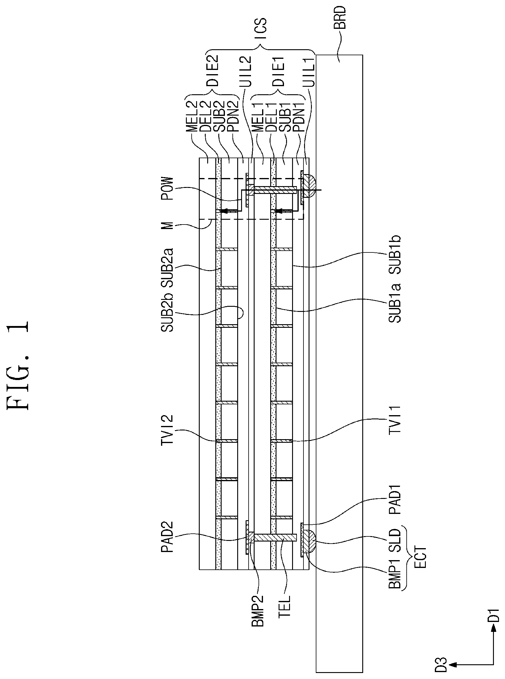
illustrates a cross-sectional view showing a semiconductor package according to some embodiments of the present inventive concept. illustrates an enlarged cross-sectional view of section M shown in , showing a three-dimensional integrated circuit structure according to some embodiments of the present inventive concept. Referring to , a three-dimensional integrated circuit structure ICS may be provided on a package substrate BRD. In some embodiments of the present inventive concept, the three-dimensional integrated circuit structure ICS may include first and second dies DIE 1 and DIE 2 . The second die DIE 2 may be stacked on the first die DIE 1 . Each of the first and second dies DIE 1 and DIE 2 may include a logic chip, a memory chip, or a radio-frequency (RF) chip. The logic chip may include a central processing unit (CPU), and the memory chip may include at least one selected from static random access memory (SRAM) cells, dynamic RAM (DRAM) cell, magnetoresistive RAM (MRAM) cells, and Flash memory cells. External connection members ECT may be provided between the three-dimensional integrated circuit structure ICS and the package substrate BRD. Each of the external connection members ECT may include a first bump BMP 1 connected to a first pad PAD 1 of the first die DIE 1 , and may also include a solder pattern SLD on the first bump BMP 1 . The three-dimensional integrated circuit structure ICS may be connected through the external connection members ECT to the package substrate BRD. A power may be applied from the package substrate BRD through the external connection members ECT to the three-dimensional integrated circuit structure ICS. A first dielectric structure UIL 1 may be provided on a first power delivery network PDN 1 . The first dielectric structure UIL 1 may cover the first bump BMP 1 . An under-fill layer may fill a space between the three-dimensional integrated circuit structure ICS and the package substrate BRD. The first die DIE 1 may include a first substrate SUB 1 . The first substrate SUB 1 may be a semiconductor substrate including silicon (Si), germanium (Ge), and silicon-germanium (SiGe). The first substrate SUB 1 may have a first surface SUB 1 a and a second surface SUB 1 b . The second surface SUB 1 b may be opposite to the first surface SUB 1 a . For example, the first surface SUB 1 a may be a top surface of the first substrate SUB 1 , and the second surface SUB 1 b may be a bottom surface of the first substrate SUB 1 . The first die DIE 1 may include the first power delivery network PDN 1 on the second surface SUB 1 b of the first substrate SUB 1 . The first power delivery network PDN 1 may provide a first device layer DEL 1 of the first die DIE 1 with a power POW transferred from the external connection member ECT. The first power delivery network PDN 1 may include a wiring network for applying the power POW to the first device layer DEL 1 . The wiring network of the first power delivery network PDN 1 may provide the first device layer DEL 1 with not only the power POW but also a signal. For example, a power delivery network according to some embodiments of the present inventive concept may include a wiring network for delivering powers and signals. The first pad PAD 1 may be provided between the first power delivery network PDN 1 and the external connection member ECT. The first pad PAD 1 may be electrically connected to the first power delivery network PDN 1 . An interlayer dielectric layer IMD may be interposed between the first power delivery network PDN 1 and the first substrate SUB 1 . The interlayer dielectric layer IMD may insulate the first power delivery network PDN 1 from the first substrate SUB 1 . The first die DIE 1 may include the first device layer DEL 1 on the first surface SUB 1 a of the first substrate SUB 1 . The first device layer DEL 1 may include one or more of passive and active elements. For example, the passive and/or active elements of the first device layer DEL 1 may include one or more of transistors, capacitors, and inductors. The passive and/or active elements of the first device layer DEL 1 may constitute at least one of logic circuits, peripheral circuits, radio frequency (RF) circuits, and complementary metal-oxide semiconductor (CMOS) circuits. The first die DIE 1 may include a first metal layer MEL 1 on the first device layer DEL 1 . The first metal layer MEL 1 may be electrically connected to the first device layer DEL 1 . As discussed below, the first metal layer MEL 1 may include a plurality of stacked metal layers. A plurality of first through vias TVI 1 that penetrate the first substrate SUB 1 may be provided between the first power delivery network PDN 1 and the first device layer DEL 1 . In some embodiments of the present inventive concept, the first through vias TVI 1 may vertically extend from the first power delivery network PDN 1 to the first metal layer MEL 1 . In some embodiments of the present inventive concept, the first through vias TVI 1 may vertically extend from the first power delivery network PDN 1 into the first metal layer MEL 1 . The first power delivery network PDN 1 may be electrically connected through the first through vias TVI 1 to the first device layer DEL 1 . The first die DIE 1 may include a plurality of through electrodes TEL that extend from the first power delivery network PDN 1 to a top surface of the first metal layer MEL 1 . The through electrode TEL may vertically extend to penetrate the first substrate SUB 1 , the first device layer DEL 1 , and the first metal layer MEL 1 . The through electrode TEL may receive a signal and the power POW from the first power delivery network PDN 1 . A plurality of second bumps BMP 2 may be provided between the first die DIE 1 and the second die DIE 2 . The second bumps BMP 2 may be correspondingly provided on top surfaces of the through electrodes TEL. The second bump BMP 2 may be connected to a second pad PAD 2 of the second die DIE 2 to electrically connect the through electrode TEL to the second die DIE 2 . The second die DIE 2 may include a second substrate SUB 2 . The second substrate SUB 2 may have a first surface SUB 2 a and a second surface SUB 2 b . The second surface SUB 2 b may be opposite to the first surface SUB 2 a. The second die DIE 2 may include a second power delivery network PDN 2 on the second surface SUB 2 b of the second substrate SUB 2 , and may also include a second device layer DEL 2 on the first surface SUB 2 a of the second substrate SUB 2 . An interlayer dielectric layer IMD may be interposed between the second power delivery network PDN 2 and the second substrate SUB 2 . The second die DIE 2 may further include a second metal layer MEL 2 on the second device layer DEL 2 . A description of the second power delivery network PDN 2 , the second device layer DEL 2 , and the second metal layer MEL 2 may be substantially the same as or similar to that of the first power delivery network PDN 1 , the first device layer DEL 1 , and the first metal layer MEL 1 , respectively. A plurality of second through vias TVI 2 that penetrate the second substrate SUB 2 may be provided between the second power delivery network PDN 2 and the second device layer DEL 2 . The second power delivery network PDN 2 may be electrically connected through the second through vias TVI 2 to the second device layer DEL 2 . The power POW may be applied from the first die DIE 1 to the second power delivery network PDN 2 through the through electrode TEL and the second bump BMP 2 . The power POW applied to the second power delivery network PDN 2 may be directly transferred through the second through via TVI 2 to the second device layer DEL 2 . As shown in , the power POW, which is applied from the external connection member ECT to the three-dimensional integrated circuit structure ICS, may be vertically transferred via the through electrode TEL. The power POW and a signal may be directly transferred to the first device layer DEL 1 and the second device layer DEL 2 through the first power delivery network PDN 1 and the second power delivery network PDN 2 that are respectively connected to lower and upper portions of the through electrode TEL. A three-dimensional integrated circuit structure ICS according to some embodiments of the present inventive concept may be configured to transfer the power POW and a signal along the shortest path (or vertical path) to the first device layer DEL 1 of the first die DIE 1 and the second device layer DEL 2 of the second die DIE 2 . Accordingly, the three-dimensional integrated circuit structure ICS may improve in power delivery efficiency and increase in electrical properties. The following will describe in detail the first die DIE 1 with reference to . The first power delivery network PDN 1 may be provided on the second surface SUB 1 b of the first substrate SUB 1 . The first power delivery network PDN 1 may include first lower lines LM 1 on the second surface SUB 1 b and second lower lines LM 2 underneath the first lower lines LM 1 . For example, the second lower line LM 2 may be located at a bottom of the first power delivery network PDN 1 . A lower via LVI may be provided between the first and second lower lines LM 1 and LM 2 . The first and second lower lines LM 1 and LM 2 may constitute a wiring network that distributes a power and a signal that are input and applies the power and the signal to the first device layer DEL 1 . The first pad PAD 1 may be provided below the second lower line LM 2 . As illustrated in , the external connection member ECT may be provided on the first pad PAD 1 . A power may be input to first power delivery network PDN 1 through the external connection member ECT and the first pad PAD 1 . The first device layer DEL 1 may be provided on the first surface SUB 1 a of the first substrate SUB 1 . The first device layer DEL 1 may include a front-end-of-line (FEOL) layer formed through an FEOL process for semiconductor fabrication. For example, the first device layer DEL 1 may include a plurality of source/drain patterns SD provided on an upper portion of the first substrate SUB 1 . The upper portion of the first substrate SUB 1 may include a first active region. The first device layer DEL 1 may include a plurality of gate electrodes GE on the first active region. For example, a plurality of gate electrodes GE may be provided on the first surface SUB 1 a of the first substrate SUB 1 . Each of the gate electrodes GE may be interposed between a pair of neighboring source/drain patterns SD. The first device layer DEL 1 may include a plurality of transistors constituted by the gate electrodes GE and the source/drain patterns SD. In some embodiments of the present inventive concept, the first device layer DEL 1 may include fin-shaped field effect transistors, also referred to as FinFETs. Is some embodiments of the present inventive concept, the first device layer DEL 1 may include three-dimensional field effect transistors, also referred to as gate-all-around FETs (GAAFETs) or multi-bridge channel FETs (MBCFETS), in which a gate surrounds a channel. The first device layer DEL 1 may further include a plurality of active contacts AC connected to corresponding source/drain patterns SD. The first device layer DEL 1 may further include a plurality of gate contacts connected to corresponding gate electrodes GE. The first metal layer MEL 1 may be provided on the first device layer DEL 1 . The first metal layer MEL 1 may include a back-end-of-line (BEOL) layer formed through a BEOL process for semiconductor fabrication. For example, the first metal layer MEL 1 may include a plurality of wiring lines M 1 , M 2 , . . . , and Mt that are sequentially stacked. For example, first wiring lines M 1 may be provided at bottom of the first metal layer MEL 1 . The first wiring lines M 1 may be connected through vias to the active contacts AC of the first device layer DEL 1 . Second wiring lines M 2 may be provided on the first wiring lines M 1 . The second wiring lines M 2 may be connected through vias to the first wiring lines M 1 . As shown in , not all of the second wiring lines M 2 are connected to the first wiring lines M 1 with the through vias. Uppermost wiring lines Mt may be provided at top of the first metal layer MEL 1 . A plurality of wiring lines may be stacked between the second wiring line M 2 and the uppermost wiring line Mt, and no limitation is imposed on the number of the stacked wiring lines between the second wiring line M 2 and the uppermost wiring line Mt. Each of the wiring lines M 1 , M 2 , . . . , and Mt of the first metal layer MEL 1 may include at least one metal selected from aluminum, copper, tungsten, molybdenum, and cobalt. The first through via TVI 1 may extend from the first lower line LM 1 of the first power delivery network PDN 1 to the first wiring line M 1 of the first metal layer MEL 1 . The first through via TVI 1 may penetrate the first substrate SUB 1 to vertically connect the first lower line LM 1 to the first wiring line M 1 . The first wiring line M 1 may be electrically connected to the source/drain pattern SD through the via and the active contact AC that are provided below the first wiring line M 1 . A power and a signal may be transferred from the first power delivery network PDN 1 via the first through via TVI 1 and the first wiring line M 1 to a transistor of the first device layer DEL 1 . The through electrode TEL may extend from the second lower line LM 2 of the first power delivery network PDN 1 to the second bump BMP 2 on the first metal layer MEL 1 . The through electrode TEL may directly contact the second lower line LM 2 and the second bump BMP 2 . The through electrode TEL may penetrate the first substrate SUB 1 , the first device layer DEL 1 , and the first metal layer MEL 1 to vertically connect the second lower line LM 2 to the second bump BMP 2 . A power may be transferred from the first power delivery network PDN 1 vertically through the first die DIE 1 to the second bump BMP 2 . The through electrode TEL may have a diameter greater than that of the first through via TVI 1 . The diameter of the through electrode TEL may decrease in a direction from lower toward upper portions of the through electrode TEL. The lower portion of the through electrode TEL may be provided in the first power delivery network PDN 1 and the upper portion of the through electrode TEL may be adjacent to the upper surface of the first die DIE 1 . For example, the lower portion of the through electrode TEL in the first power delivery network PDN 1 may have a first diameter DI 1 . The upper portion of the through electrode TEL in the first metal layer MEL 1 may have a second diameter DI 2 . The second diameter DI 2 may be less than the first diameter DI 1 . A dielectric spacer CSP may be provided on a sidewall of the through electrode TEL. The dielectric spacer CSP may include a silicon-based dielectric material, such as silicon oxide or silicon nitride. The dielectric spacer CSP may insulate the sidewall of the through electrode TEL. A dielectric spacer may also be provided on and insulate a sidewall of the first through via TVI 1 . A second dielectric structure UIL 2 may be provided on the first metal layer MEL 1 . The second dielectric structure UIL 2 may include a first dielectric layer PAL 1 and a second dielectric layer PAL 2 on the first dielectric layer PAL 1 . The second dielectric structure UIL 2 may include an opening OPN that exposes the top surface of the through electrode TEL. For example, the first dielectric layer PAL 1 may include an inorganic dielectric layer, such as a silicon nitride layer, a silicon oxide layer, or a silicon oxynitride layer. The second dielectric layer PAL 2 may include an organic polymer layer. For example, the organic polymer layer may include polyimide, fluorocarbon, resin, or synthetic rubber. The second bump BMP 2 may be provided in the opening OPN of the second dielectric structure UIL 2 . The second bump BMP 2 may have a bottom surface in contact with the top surface of the through electrode TEL. The second bump BMP 2 may have a top surface in contact with the second pad PAD 2 of the second die DIE 2 . Thus, power may be transmitted via the second bump BMP 2 from the through electrode TEL to the second pad PAD 2 . The following will describe the second die DIE 2 . The second die DIE 2 may be provided on the second dielectric structure UIL 2 . The second dielectric structure UIL 2 and the second bump BMP 2 may be interposed between the first die DIE 1 and the second die DIE 2 . The second power delivery network PDN 2 may be provided on the second surface SUB 2 b of the second substrate SUB 2 . The second power delivery network PDN 2 may include first lower lines LM 1 on the second surface SUB 2 b of the second substrate SUB 2 and second lower lines LM 2 below the first lower lines LM 1 . The first and second lower lines LM 1 and LM 2 may constitute a wiring network that distributes a power and a signal that are input and applies the power and the signal to the second device layer DEL 2 . The second pad PAD 2 may be provided below the second lower line LM 2 . The second pad PAD 2 may be in contact with the second bump BMP 2 to electrically connect to the through electrode TEL of the first die DIE 1 . A power may be input to the second power delivery network PDN 2 through the through electrode TEL and the second pad PAD 2 . The second device layer DEL 2 may be provided on the first surface SUB 2 a of the second substrate SUB 2 . The second device layer DEL 2 may include an FEOL layer formed through an FEOL process for semiconductor fabrication. For example, the second device layer DEL 2 may include a, plurality of source/drain patterns SD provided on an upper portion of the second substrate SUB 2 . The upper portion of the second substrate SUB 2 may include a second active region. The second device layer DEL 2 may include a plurality of gate electrodes GE on the second active region. In some embodiments of the present inventive concept, the second device layer DEL 2 may include fin-shaped field effect transistors, e.g., FinFETs. Is some embodiments of the present inventive concept, the second device layer DEL 2 may include three-dimensional field effect transistors, GAAFETs or MBCFETS, in which a gate surrounds a channel. The second device layer DEL 2 may further include a plurality of active contacts AC connected to corresponding source/drain patterns SD. The second device layer DEL 2 may further include a plurality of gate contacts connected to corresponding gate electrodes GE. The second metal layer MEL 2 may be provided on the second device layer DEL 2 . The second metal layer MEL 2 may include a BEOL layer formed through a BEOL process for semiconductor fabrication. For example, the second metal layer MEL 2 may include a plurality of wiring lines M 1 , M 2 , . . . , and Mt that are sequentially stacked. A detailed description of the second metal layer MEL 2 may be substantially the same as or similar to that of the first metal layer MEL 1 discussed above. The second lower line LM 2 of the second power delivery network PDN 2 may be connected to the second pad PAD 2 , and as a result, a power may be transferred from the first die DIE 1 via the through electrode TEL to the second power delivery network PDN 2 of the second die DIE 2 . The second through via TVI 2 may be provided to extend from the first lower line LM 1 of the second power delivery network PDN 2 to the first wiring line M 1 of the second metal layer MEL 2 . The second through via TVI 2 may be directly connected to the first lower line LM 1 of the second power delivery network PDN 2 and the first wiring line M 1 of the second metal layer MEL 2 . The second through via TVI 2 may penetrate the second substrate SUB 2 to vertically connect the first lower line LM 1 to the first wiring line M 1 . Thus, a power and a signal may be transferred from the second power delivery network PDN 2 via the second through via TVI 2 and the first wiring line M 1 to a transistor of the second device layer DEL 2 . to 7 illustrate cross-sectional views of section M shown in , showing a method of fabricating a three-dimensional integrated circuit structure according to some embodiments of the present inventive concept. Referring to , an FEOL process for semiconductor fabrication may be performed to form a first device layer DEL 1 on a first surface SUB 1 a of a first substrate SUB 1 . For example, a plurality of source/drain patterns SD may be formed in a first active region AR 1 of the first substrate SUB 1 . A plurality of gate electrodes GE may be formed on the first active region AR 1 . A plurality of active contacts AC may be formed to connect to corresponding source/drain patterns SD. A BEOL process for semiconductor fabrication may be performed to form a first metal layer MEL 1 on the first device layer DEL 1 . For example, the formation of the first metal layer MEL 1 may include sequentially forming (or stacking) a plurality of wiring lines M 1 , M 2 , . . . , and Mt. In some embodiments of the present inventive concept, an aluminum pad may be formed on an uppermost wiring line Mt on the first metal layer MEL 1 . Referring to , the first die DIE 1 that has undergone the BEOL process may be reversed (e.g., flipped) to expose a, 6 second surface SUB 1 b of the first substrate SUB 1 . In some embodiments of the inventive concept, the second surface SUB 1 b of the first substrate SUB 1 may undergo a chemical mechanical polishing (CMP) process to reduce a thickness of the first substrate SUB 1 . The second surface SUB 1 b of the first substrate SUB 1 may undergo an anisotropic etching process to form a through via hole VIH that penetrates the first substrate SUB 1 . The etching process may continue until the through via hole VIH exposes a first wiring line M 1 . The through via hole VIH may be filled with a conductive material to from a first through via TVI 1 . The first through via TVI 1 may have a bottom surface in direct contact with the first wiring line M 1 . The first through via TVI 1 may have a top surface that is exposed on the second surface SUB 1 b. A semiconductor process may be performed to form a first power delivery network PDN 1 on the second surface SUB 1 b of the first substrate SUB 1 . For example, a first lower dielectric layer LIL 1 may be formed on the second surface SUB 1 b . A plurality of first lower lines LM 1 may be formed in the first lower dielectric layer LIL 1 . At least one of the first lower lines LM 1 may be formed on the first through via TVI 1 to contact the top surface of the first through via TVI 1 . For example, the first lower line LM 1 may be electrically connected through the first through via TVI 1 to the first wiring line M 1 . An interlayer dielectric layer IMD may be interposed between the first power delivery network PDN 1 and the first substrate SUB 1 . Referring to , a second lower dielectric layer LIL 2 may be formed on the first lower dielectric layer LIL 1 . The second lower dielectric layer LIL 2 may undergo an anisotropic etching process to form a through electrode hole VEH that penetrates the first substrate SUB 1 , the first device layer DEL 1 , and the first metal layer MEL 1 . The etching process may continue until the through electrode hole VEH completely penetrates the first metal layer MEL 1 . The through electrode hole VEH may be formed to have a diameter that decreases in a third direction D 3 . For example, the through electrode hole VEH in the first power delivery network PDN 1 may have a third diameter DI 3 , and the through electrode hole VEH in the first metal layer MEL 1 may have a fourth diameter DI 4 . The third diameter DI 3 may be greater than the fourth diameter DI 4 . A dielectric spacer CSP may be conformally formed on an inner sidewall of the through electrode hole VEH. The dielectric spacer CSP may include a dielectric material. A through electrode TEL may be formed on the dielectric spacer CSP to completely fill the through electrode hole VEH. For example, a barrier layer and a conductive layer may be sequentially formed on the dielectric spacer CSP. The barrier layer may include a metal nitride layer or a combination of a metal layer and a metal nitride layer. The metal nitride layer may include at least one selected from a titanium nitride (TiN) layer, a tantalum nitride (TaN) layer, a tungsten nitride (WN) layer, a nickel nitride (NiN) layer, a cobalt nitride (CoN) layer, and a platinum nitride (PtN) layer. The metal layer may include at least one metal selected from aluminum, copper, tungsten, molybdenum, and cobalt. A second lower line LM 2 may be formed on the through electrode TEL. The second lower line LM 2 may be formed in the second lower dielectric layer LIL 2 . The second lower line LM 2 may be connected to the through electrode TEL. For example, the second lower line LM 2 may directly contact the through electrode TEL. In addition, the second lower line LM 2 may be connected to the first lower line LM 1 . For example, the second lower line LM 2 may be connected to the first lower line LM 1 through a first lower via LV 1 . Referring to , the first die DIE 1 may be reversed again to re-expose the first metal layer MEL 1 . A second bump BMP 2 may be formed on an exposed top surface of the through electrode TEL. For example, the second bump BMP 2 may be formed through a post-fabrication process. The formation of the second bump BMP 2 may include forming a seed pattern on the exposed top electrode TEL and performing a plating process on the seed pattern to form a conductive pattern. The seed pattern and the conductive pattern may constitute the second bump BMP 2 . For example, the seed pattern may include a conductive material, such as copper, titanium, and any alloy thereof. The conductive pattern may include copper. Referring to , a second die DIE 2 may be formed. The formation of the second die DIE 2 may be substantially the same as the formation of the first die DIE 1 discussed above with reference to to 6 . The formation of the through electrode TEL may be omitted in forming the second die DIE 2 . A second dielectric structure UIL 2 may be formed on a second power delivery network PDN 2 of the second die DIE 2 . The second dielectric structure UIL 2 may be patterned to form an opening OPN that exposes a second pad PAD 2 . The second die DIE 2 may be stacked on the first die DIE 1 , such that the first die DIE 1 and the second die DIE 2 may be bonded to each other. The second bump BMP 2 may be provided in the opening OPN to thereby contact the second pad PAD 2 . As a result, the first power delivery network PDN 1 of the first die DIE 1 may be electrically connected via the through electrode TEL to the second power delivery network PDN 2 of the second die DIE 2 . In some embodiments of the present inventive concept, referring back to , a three-dimensional integrated circuit structure ICS including the first die DIE 1 and the second die DIE 2 may be mounted on a package substrate BRD. For example, an external connection member ECT may be formed on the first pad PAD 1 of the three-dimensional integrated circuit structure ICS, and the three-dimensional integrated circuit structure ICS may be connected through the external connection member ECT to the package substrate BRD. illustrates a cross-sectional view showing a semiconductor package according to some embodiments of the present inventive concept. illustrates an enlarged cross-sectional view of sections N and M shown in , showing a three-dimensional integrated circuit structure according to some embodiments of the present inventive concept. In the embodiment that follows, a detailed description of features repetitive to those discussed above with reference to may be omitted, and a difference thereof will mainly be discussed in detail. Referring to , a third pad PAD 3 may be provided at top of the three-dimensional integrated circuit structure ICS. The third pad PAD 3 may be provided on the second metal layer MEL 2 of the second die DIE 2 . The third pad PAD 3 may be directly connected to the second metal layer MEL 2 . A signal connection member SCT may be connected to connect the third pad PAD 3 to the package substrate BRD. In some embodiments of the present inventive concept, the signal connection member SCT may include a conductive wire. The signal connection member SCT may provide an input or output between the package substrate BRD and the third pad PAD 3 . The second die DIE 2 may include a plurality of through contacts TCNT that extend from the second metal layer MEL 2 to a bottom surface of the second power delivery network PDN 2 . The through contacts TCNT may extend in the third direction D 3 to penetrate the second power delivery network PDN 2 , the second substrate SUB 2 , the second device layer DEL 2 , and a lower portion of the second metal layer MEL 2 . The through contact TCNT may receive a signal from the second metal layer MEL 2 . A plurality of third bumps BMP 3 may be provided between the first die DIE 1 and the second die DIE 2 . The third bumps BMP 3 may be correspondingly provided on bottom surfaces of the through contacts TCNT. The third bump BMP 3 may be connected to the first metal layer MEL 1 to electrically connect the through contact TCNT to the first die DIE 1 . A signal may be transferred from the second metal layer MEL 2 of the second die DIE 2 through the third bump BMP 3 and the through contact TCNT to the first metal layer MEL 1 of the first die DIE 1 . Therefore, a signal may be exchanged and processed between the first die DIE 1 and the second die DIE 2 . The three-dimensional integrated circuit structure ICS according to some embodiments of the present inventive concept may be configured to transfer a signal along the shortest path between the first metal layer MEL 1 of the first die DIE 1 and the second metal layer MEL 2 of the second die DIE 2 . Accordingly, the three-dimensional integrated circuit structure ICS may increase in signal processing speed and electrical properties. The first die DIE 1 and the second die DIE 2 will be discussed in detail with reference to . The through contact TCNT may be provided to vertically extend from the uppermost wiring line Mt of the second metal layer MEL 2 to the third bump BMP 3 between the first die DIE 1 and the second die DIE 2 . The through contact TCNT may penetrate the second power delivery network PDN 2 , the second substrate SUB 2 , and the second device layer DEL 2 to vertically connect the second metal layer MEL 2 to the third bump BMP 3 . For example, a signal processed in the second device layer DEL 2 of the second die DIE 2 may be transferred to the third bump BMP 3 through the second metal layer MEL 2 and the through contact TCNT. The third bump BMP 3 may be connected to the uppermost wiring line Mt of the first metal layer MEL 1 via the through contact TCNT. Therefore, the signal may be input through the first metal layer MEL 1 to the first device layer DEL 1 . Accordingly, a signal may be exchanged and processed between the first die DIE 1 and the second die DIE 2 . A variation in diameter of the through contact TCNT may be the same as or similar to a variation in diameter of the through electrode TEL. The through contact TCNT may have a diameter that decreases in a direction from lower toward upper portions thereof. For example, the lower portion of the through contact TCNT in the second power delivery network PDN 2 may have a fifth diameter DI 5 . The upper portion of the through contact TCNT in the second metal layer MEL 2 may have a sixth diameter DI 6 . The sixth diameter DI 6 may be less than the fifth diameter DI 5 . illustrates a cross-sectional view showing a semiconductor package according to some embodiments of the present inventive concept. In the embodiment that follows, a detailed description of features repetitive to those discussed above with reference to may be omitted, and a difference thereof will mainly be discussed in detail. Referring to , the three-dimensional integrated circuit structure ICS according to some embodiments of the present inventive concept may further include a third die DIE 3 interposed between the first die DIE 1 and the second die DIE 2 . The third die DIE 3 may include a third power delivery network PDN 3 , a third substrate SUB 3 , a third device layer DEL 3 , and a third metal layer MEL 3 that are sequentially stacked. The third power delivery network PDN 3 , the third substrate SUB 3 , the third device layer DEL 3 , and the third metal layer MEL 3 of the third die DIE 3 may be respectively the same as or similar to the first power delivery network PDN 1 , the first substrate SUB 1 , the first device layer DEL 1 , and the first metal layer MEL 1 of the first die DIE 1 discussed above with reference to . The third die DIE 3 may further include second through electrodes TEL 2 that penetrate therethrough. The second through electrode TEL 2 may be substantially the same as the through electrode TEL of the first die DIE 1 discussed above with reference to . The second through electrode TEL 2 may extend in the third direction D 3 from the third power delivery network PDN 3 to a top surface of the third metal layer MEL 3 . The second through electrode TEL 2 may be electrically connected to the first through electrode TEL 1 of the first die DIE 1 . For example, the first through electrode TEL 1 may be electrically connected to the third power delivery network PDN 3 through the second bump BMP 2 and the third pad PAD 3 in direct contact with the second bump BMP 2 . The second through electrode TEL 2 may be connected to the third power delivery network PDN 3 , and the power POW applied to the third power delivery network PDN 3 may be transferred in the third direction D 3 through the second through electrode TEL 2 . The second through electrode TEL 2 may be electrically connected to the second power delivery network PDN 2 through the second bump BMP 2 and the second pad PAD 2 in direct contact with the second bump BMP 2 . As a result, the power POW applied from the external connection member ECT to the three-dimensional integrated circuit structure ICS may be transferred in a vertical direction (e.g., the third direction D 3 ) through the first through electrode TEL 1 and the second through electrode TEL 2 . The first and second through electrodes TEL 1 and TEL 2 may be electrically connected to the first, second, and third power delivery networks PDN 1 , PDN 2 , and PDN 3 , and the power POW and a signal may be directly transferred to the first, second, and third device layers DEL 1 , DEL 2 , and DEL 3 through the first, second, and third power delivery networks PDN 1 , PDN 2 , and PDN 3 . In some embodiments of the present inventive concept, the second through electrode TEL 2 may vertically overlap the first through electrode TELL. The second pad PAD 2 may vertically overlap the third pad PAD 3 . In some embodiments of the present inventive concept, there may be provided a plurality of third dies DIE 3 that are stacked. Each of the plurality of third dies DIE 3 may include the third power delivery network PDN 3 and the second through electrode TEL 2 . Thus, the power POW may be transferred from the first die DIE 1 through the stacked third dies DIE 3 to the second die DIE 2 at top position of the three-dimensional integrated circuit structure ICS. For example, the N number of the third dies DIE 3 may be interposed between the first die DIE 1 and the second die DIE 2 , and N may be an integer between 1 and 10. , 12 , and 13 illustrate enlarged cross-sectional views of section M shown in , showing a three-dimensional integrated circuit structure according to some embodiments of the present inventive concept. In the embodiment that follows, a detailed description of features repetitive to those discussed above with reference to may be omitted, and a difference thereof will mainly be discussed in detail. Referring to , the first die DIE 1 may include neither the first power delivery network PDN 1 nor the first through vias TVI 1 . The external connection member ECT, such as a bump, may be directly provided on the second surface SUB 1 b of the first substrate SUB 1 . The through electrode TEL may directly connect the external connection member ECT to the second bump BMP 2 between the first die DIE 1 and the second die DIE 2 . Referring to , a third substrate SUB 3 may be interposed between the first die DIE 1 and the second die DIE 2 . The third substrate SUB 3 may be a semiconductor wafer used as a carrier substrate. For example, the third substrate SUB 3 may include silicon (Si). A bonding layer BDL may be provided between the third substrate SUB 3 and the first die DIE 1 . Referring to , the active contact AC of the first die DIE 1 may include a pad part PDP at an upper portion thereof. The pad part PDP may horizontally extend to overlap the first through via TVI 1 . The first through via TVI 1 may be directly connected to the pad part PDP of the active contact AC. Therefore, a power and a signal may be directly transferred to the active contact AC from the first power delivery network PDN 1 . The second die DIE 2 may include a MOL line M 0 between the active contact AC and the first wiring line M 1 . The MOL line M 0 may be formed through a middle-of-line (MOL) process before the formation of the first wiring line M 1 . The MOL line M 0 may horizontally extend to overlap the second through via TVI 2 . The second through via TVI 2 may be directly connected to the MOL line M 0 . Therefore, a power and a signal may be directly transferred from the second power delivery network PDN 2 to the MOL line M 0 below the first wiring line Mt. As a result, there may be a reduction in path through which a power and a signal are transferred to the second device layer DEL 2 . illustrates an enlarged cross-sectional view of sections N and M shown in , showing a three-dimensional integrated circuit structure according to some embodiments of the present inventive concept. In the embodiment that follows, a detailed description of features repetitive to those discussed above with reference to may be omitted, and a difference thereof will mainly be discussed in detail. Referring to , the second die DIE 2 may include a first through contact TCNT 1 and a second through contact TCNT 2 . The first through contact TCNT 1 may vertically extend from the second metal layer MEL 2 to the second surface SUB 2 b of the second substrate SUB 2 . The second through contact TCNT 2 may vertically extend from the second surface SUB 2 b of the second substrate SUB 2 to a top surface of the third bump BMP 3 . The second through contact TCNT 2 may vertically overlap the first through contact TCNT 1 . The second through contact TCNT 2 may be connected to the first through contact TCNT 1 . The third bump BMP 3 and the second metal layer MEL 2 may be electrically connected to each other through the first and second through contacts TCNT 1 and TCNT 2 . A variation in diameter of the first through contact TCNT 1 may be opposite to a variation in diameter of the through electrode TEL. The first through contact TCNT 1 may have a diameter that increases in a direction from lower toward upper portions thereof. For example, a fifth diameter DI 5 may be given to the lower portion of the first through contact TCNT 1 in the second substrate SUB 2 . A sixth diameter DI 6 may be given to the upper portion of the first through contact TCNT 1 in the second metal layer MEL 2 . The sixth diameter DI 6 may be greater than the fifth diameter DI 5 . In a three-dimensional integrated circuit structure according to some embodiments of the present inventive concept, a power delivery network and its connected through electrode may be used to directly transfer an external power along the shortest path to a first device layer of a first die and a second device layer of a second die. The three-dimensional integrated circuit structure may increase in electrical properties and improve in power and signal delivery efficiency. Although some embodiments of the present inventive concept have been described with reference to the accompanying figures, it will be understood that various changes in form and detail may be made thereto without departing from the spirit and scope of the present inventive concept as set forth in the appended claims. It therefore will be understood that the embodiments described above are illustrative and not limiting.
Figures (14)
Citations
This patent cites (23)
- US8513061
- US9536809
- US9654004
- US9741691
- US10128301
- US10950546
- US10978348
- US11041211
- US2002/0020862
- US2009/0160050
- US2010/0001379
- US2010/0252934
- US2011/0298130
- US2012/0238069
- US2012/0292777
- US2016/0322331
- US2020/0373331
- US2021/0118805
- US2021/0143127
- US2023/0060355
- US10-2011-0134198
- US10-2015-0066527
- US202133444