Semiconductor Package Including Metal Pattern Layer with Open Region Which Overlaps Non-contact Pad
Abstract
A semiconductor package includes: a package substrate including a plurality of insulating layers and a plurality of metal pattern layers respectively disposed on the plurality of insulating layers, wherein each of the plurality of metal pattern layers has an interconnection layer; at least one semiconductor chip disposed on an upper surface of the package substrate, and connected to the interconnection layer; contact pads disposed on a lower surface of the package substrate, and connected to the interconnection layer; and non-contact pads disposed on the lower surface of the package substrate, and insulated from the interconnection layer, wherein a lowermost metal pattern layer among the plurality of metal pattern layers has a first open region at least partially overlapping at least one non-contact pad among the non-contact pads, in a direction perpendicular to the upper surface of the package substrate.
Claims (20)
1 . A semiconductor package, comprising: a package substrate including a plurality of insulating layers and a plurality of metal pattern layers respectively disposed on the plurality of insulating layers, wherein each of the plurality of metal pattern layers has an interconnection layer; at least one semiconductor chip disposed on an upper surface of the package substrate, and connected to the interconnection layer; contact pads disposed on a lower surface of the package substrate, and connected to the interconnection layer; and non-contact pads disposed on the lower surface of the package substrate, and insulated from the interconnection layer, wherein a lowermost metal pattern layer among the plurality of metal pattern layers has a first open region at least partially overlapping a central portion of at least one non-contact pad among the non-contact pads, in a direction perpendicular to the upper surface of the package substrate.
14 . A semiconductor package, comprising: a package substrate including a plurality of insulating layers and a plurality of metal pattern layers respectively disposed on the plurality of insulating layers, wherein each of the plurality of metal pattern layers has an interconnection layer; a first semiconductor chip disposed on first surface of the package substrate, and connected to the interconnection layer; a second semiconductor chip disposed on the first surface of the package substrate, and connected to the interconnection layer; contact pads disposed on a second surface of the package substrate, and connected to the interconnection layer, wherein the contact pads include first and second signal pads for transmitting a differential signal, and non-contact pads disposed on the second surface of the package substrate, and insulated from the interconnection layer, wherein the non-contact pads comprise at least one non-contact pad disposed adjacent to the second signal pad and positioned closer to an edge of the package substrate than the second signal pad, wherein a first metal pattern layer among the plurality of interconnection layers has an open region overlapping the at least one non-contact pad among the non-contact pads in a direction perpendicular to the first surface of the package substrate.
19 . A semiconductor package, comprising: a package substrate having a plurality of insulating layers and a plurality of metal pattern layers respectively disposed on the plurality of insulating layers, wherein each of the plurality of metal pattern layers has an interconnection layer; at least one semiconductor chip disposed on an upper surface of the package substrate, and connected to the interconnection layer; contact pads disposed on a lower surface of the package substrate, and connected to the interconnection layer, wherein the contact pads include a first signal pad and a second signal pad for transmitting a differential signal; non-contact pads disposed on the lower surface of the package substrate, and insulated from the interconnection layer; contact bumps respectively disposed on the contact pads; and non-contact bumps respectively disposed on the non-contact pads, wherein a lowermost metal pattern layer among the plurality of interconnection layers has an open region at least partially overlapping at least one non-contact pad among the non-contact pads.
Show 17 dependent claims
2 . The semiconductor package of claim 1 , wherein the lowermost metal pattern layer comprises a ground pattern, and the first open region is located in the ground pattern.
3 . The semiconductor package of claim 2 , wherein the first open region is a hole in the ground pattern.
4 . The semiconductor package of claim 1 , wherein the first open region has an area greater than an area of the at least one non-contact pad.
5 . The semiconductor package of claim 1 , wherein a next lowermost metal pattern layer among the plurality of metal pattern layers is disposed on the lowermost metal pattern layer and has at least one second open region overlapping the at least one non-contact pad in the vertical direction.
6 . The semiconductor package of claim 1 , wherein the at least one non-contact pad is positioned between one of the contact pads and an edge of the package substrate.
7 . The semiconductor package of claim 6 , wherein the contact pads comprise first and second signal pads for transmitting a differential signal, and the one contact pad is one of the first or second signal pads.
8 . The semiconductor package of claim 7 , wherein the other one of the first or second signal pads is disposed closer to the edge of the package substrate than the one of the first or second signal pads.
9 . The semiconductor package of claim 8 , wherein the at least one non-contact pad and the other one of the first or second signal pads are disposed side by side at the edge of the package substrate.
10 . The semiconductor package of claim 1 , wherein an insulating layer between the lowermost metal pattern layer and the non-contact pads has a thickness of about 20 μm or less.
11 . The semiconductor package of claim 1 , further comprising conductive bumps respectively disposed on the contact pads and the non-contact pads.
12 . The semiconductor package of claim 1 , wherein the at least one semiconductor chip comprises a plurality of semiconductor chips.
13 . The semiconductor package of claim 12 , wherein the plurality of semiconductor chips comprise a memory chip and a processor chip for controlling an operation of the memory chip.
15 . The semiconductor package of claim 14 , wherein the first signal pad is disposed closer to the edge of the package substrate than the second signal pad.
16 . The semiconductor package of claim 15 , wherein the at least one non-contact pad and the first signal pad are disposed side by side at the edge of the package substrate.
17 . The semiconductor package of claim 14 , wherein the first semiconductor chip comprises a memory device, and the second semiconductor chip comprises a processor chip configured to transmit/receive data to and from the memory device and to and from an external device using a serial interface.
18 . The semiconductor package of claim 17 , wherein the semiconductor package is a universal flash storage (UFS) device.
20 . An electronic device, comprising: a circuit board having circuit lines; and the semiconductor package of claim 19 disposed on the circuit board, wherein the circuit lines comprise a first signal line and a second signal line, wherein the first signal line is connected to a contact bump disposed on the first signal pad, and the second signal line is connected to a contact bump disposed on the second signal pad and is connected to a non-contact bump disposed on the at least one non-contact pad.
Full Description
Show full text →
CROSS-REFERENCE TO RELATED APPLICATION
This application claims benefit of priority under 35 U.S.C. 119(a) to Korean Patent Application No. 10-2022-0020608 filed on Feb. 17, 2022, in the Korean Intellectual Property Office, the disclosure of which is incorporated by reference herein in its entirety.
TECHNICAL FIELD
The present inventive concept relates to a semiconductor package. More particularly, the present inventive concept relates to a semiconductor package including a metal pattern layer having an open region.
DISCUSSION OF THE RELATED ART
According to the development of the electronics industry and the desires of users, electronic devices are becoming lighter, thinner, and smaller. According to this trend, it is increasing desirable for semiconductor packages used in electronic devices to have high performance (e.g., high speed) and high capacitance. In addition, as an example, the semiconductor package may be provided as a Ball Grid Array (BGA) package to be mounted on an electronic device.
When a semiconductor package is mounted on a main board of an electronic device, characteristic degradation may occur due to conductive bumps (e.g., balls) connected to a signal line of the main board.
SUMMARY
According to an example embodiment of the present inventive concept, a semiconductor package includes: a package substrate including a plurality of insulating layers and a plurality of metal pattern layers respectively disposed on the plurality of insulating layers, wherein each of the plurality of metal pattern layers has an interconnection layer; at least one semiconductor chip disposed on an upper surface of the package substrate, and connected to the interconnection layer; contact pads disposed on a lower surface of the package substrate, and connected to the interconnection layer; and non-contact pads disposed on the lower surface of the package substrate, and insulated from the interconnection layer, wherein a lowermost metal pattern layer among the plurality of metal pattern layers has a first open region at least partially overlapping at least one non-contact pad among the non-contact pads, in a direction perpendicular to the upper surface of the package substrate.
According to an example embodiment of the present inventive concept, a semiconductor package includes: a package substrate including a plurality of insulating layers and a plurality of metal pattern layers respectively disposed on the plurality of insulating layers, wherein each of the plurality of metal pattern layers has an interconnection layer; a first semiconductor chip disposed on first surface of the package substrate, and connected to the interconnection layer; a second semiconductor chip disposed on the first surface of the package substrate, and connected to the interconnection layer; contact pads disposed on a second surface of the package substrate, and connected to the interconnection layer, wherein the contact pads include first and second signal pads for transmitting a differential signal; and non-contact pads disposed on the second surface of the package substrate, and insulated from the interconnection layer, wherein the non-contact pads include at least one non-contact pad disposed adjacent to the second signal pad and positioned closer to an edge of the package substrate than the second signal pad, wherein a first metal pattern layer among the plurality of interconnection layers has an open region overlapping the at least one non-contact pad among the non-contact pads in a direction perpendicular to the first surface of the package substrate.
According to an example embodiment of the present inventive concept, a semiconductor package includes: a package substrate having a plurality of insulating layers and a plurality of metal pattern layers respectively disposed on the plurality of insulating layers, wherein each of the plurality of metal pattern layers has an interconnection layer; at least one semiconductor chip disposed on an upper surface of the package substrate, and connected to the interconnection layer; contact pads disposed on a lower surface of the package substrate, and connected to the interconnection layer, wherein the contact pads include a first signal pad and a second signal pad for transmitting a differential signal; non-contact pads disposed on the lower surface of the package substrate, and insulated from the interconnection layer; contact bumps respectively disposed on the contact pads; and non-contact bumps respectively disposed on the non-contact pads, wherein a lowermost metal pattern layer among the plurality of interconnection layers has an open region at least partially overlapping at least one non-contact pad among the non-contact pads.
BRIEF DESCRIPTION OF DRAWINGS
The above and other aspects of the present inventive concept will become more apparent by describing in detail embodiments thereof, with reference to the accompanying drawings, in which:
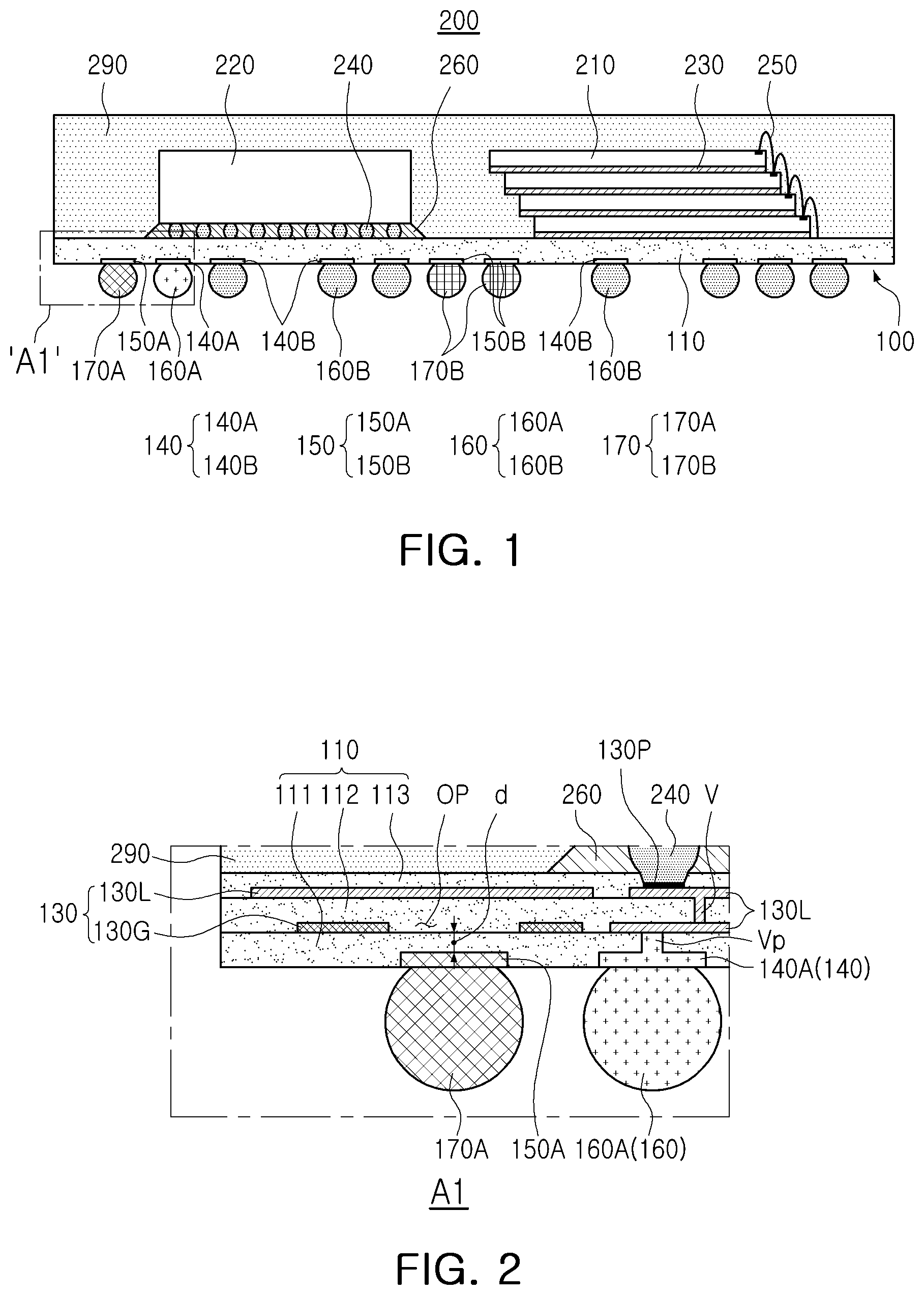
is a cross-sectional view illustrating a semiconductor package according to an example embodiment of the present inventive concept.
is a partially enlarged view of portion (“A 1 ”) of the semiconductor package of .
is a cross-sectional view illustrating a circuit board on which the semiconductor package of is mounted.
is a partial enlarged view illustrating an enlarged portion “A 2 ” of .
is a plan view illustrating signal routing of a circuit board on which a semiconductor package is mounted and an arrangement of conductive bumps in the semiconductor package according to an embodiment of the present inventive concept.
are partial plan views illustrating portion “A 3 ” of at a first level LV 1 and a second level LV 2 , respectively.
is a plan view illustrating a portion of a package substrate of a semiconductor package according to an example embodiment of the present inventive concept.
is a graph illustrating delivery characteristics according to the introduction of an example embodiment of the present inventive concept.
is a cross-sectional view illustrating a semiconductor package according to an example embodiment of the present inventive concept, and is an enlarged partial view of portion (“B 1 ”) of the semiconductor package of .
is a cross-sectional view illustrating a semiconductor package according to an example embodiment of the present inventive concept, and is an enlarged partial view of portion (“B 2 ”) of the semiconductor package of .
DETAILED DESCRIPTION OF THE EMBODIMENTS
Hereinafter, example embodiments of the present inventive concept will be described in detail with reference to the accompanying drawings.
is a cross-sectional view illustrating a semiconductor package according to an example embodiment of the present inventive concept, and is an enlarged partial view of portion (“A 1 ”) of the semiconductor package of .
Referring to , a semiconductor package 200 includes a package substrate, and a first semiconductor chip and a second semiconductor chip disposed on the package substrate.
The package substrate 100 may include a body portion 110 , a plurality of metal pattern layers 130 , contact pads 140 , and non-contact pads 150 . The body portion 110 may have a plurality of insulating layers 111 , 112 , and 113 , and a plurality of metal pattern layers 130 may be respectively disposed on the plurality of insulating layers 111 , 112 , and 113 . The contact pads 140 and non-contact pads 150 may be disposed on a lower surface of the body portion 101 . Here, the plurality of metal pattern layers 130 may include interconnection layers 130 L and ground pattern layers 130 G. The interconnection layers 130 L may be interconnected to each other by a via V, and may constitute a redistribution circuit. The contact pads 140 may be connected to the interconnection layers 130 L by a pad via Vp, and the non-contact pads 150 might not be connected to the interconnection layer 130 L and may be separated from the redistribution circuit.
For example, the package substrate 100 may be a printed circuit board. The package substrate 100 is not limited to a printed circuit board, and may be interconnection substrate of various types.
The package substrate 100 may be made of at least one of a phenol resin, an epoxy resin, and a polyimide. For example, the package substrate 100 may include FR4, tetrafunctional epoxy, polyphenylene ether, epoxy/polyphenylene oxide, bismaleimidetriazine (BT), Thermount, cyanate ester, polyimide, and/or liquid crystal polymer. In addition, the metal pattern layer 130 , the contact pads 140 , and the non-contact pads 150 may include, for example, copper (Cu), nickel (Ni), aluminum (Al), and/or beryllium copper.
Conductive bumps 160 and 170 may be formed on the contact pads 140 and the non-contact pads 150 of the package substrate 100 , respectively. The conductive bumps 160 and 170 may include, for example, a solder ball, and the semiconductor package 200 may be a ball grid array (BGA) package.
The contact pads 140 , which are connected to the interconnection layer 130 L, may include a first contact pad 140 A and a second contact pad 140 B. The first contact pad 140 A transmits a signal that is relatively sensitive to impedance, and the second contact pad 140 B transmits a power signal or a ground signal. First and second contact bumps 160 A and 160 B may be disposed on the first and second contact pads 140 A and 140 B, respectively.
As described above, in the non-contact pad 150 connected to the wiring layer 130 L, similar to the contact bump 160 , a non-contact bump 170 may be disposed on the non-contact pad 150 , and as illustrated in , stable support of the semiconductor package 200 on a main board (see ) may be achieved.
In the present example embodiment, the non-contact pad 150 may be divided into a first non-contact pad 150 A and a second non-contact pad 150 B depending on whether it is connected to a signal line of the main board. Similarly thereto, the non-contact bump 170 may be divided into first and second non-contact bumps 170 A and 170 B, which are respectively disposed on the first and second non-contact pads 150 A and 150 B.
is a cross-sectional view illustrating a circuit board 310 on which the semiconductor package 200 of is mounted, and is a partially enlarged view illustrating portion “A 2 ” of . The electronic device 300 illustrated in may be, for example, an electronic device having a memory device such as a universal flash storage (UFS) card.
Referring to , the first non-contact pad 150 A may be electrically connected to the same signal line 315 B as the first contact pad 140 A through the first non-contact bump 170 A. Here, the first non-contact pad 150 A and the first non-contact bump 170 A may serve as stubs of the signal line 315 B.
In the present embodiment, to reduce the stub influence due to the first non-contact bump 170 A, an open region OP may be included in a metal pattern layer 130 (e.g., a lowermost metal pattern) that is disposed on a lowermost insulating layer 111 . For example, the lowermost metal pattern layer 130 may be disposed on the lowermost insulating layer 111 in a direction substantially perpendicular to an upper surface of the package substrate 100 .
By reducing capacitance generated in the first non-contact bump 170 A by the open region OP, an influence of the stub on the first non-contact bump 170 A can be reduced. As a thickness d of the lowermost insulating layer 111 decreases, capacitance due to the adjacent metal pattern layer may increase, so that the influence of the impedance caused by the formation of the open region OP can be effectively reduced. For example, when the thickness d of the lowermost insulating layer 111 is about 20 μm or less, for example, about 15 μm or less, an effect of the formation of the open region OP may be expected.
The open region OP may have a larger than a planar area of the first non-contact pad 150 A. In an example embodiment of the present inventive concept, the metal pattern layer on which the open region OP is formed may be a ground pattern 130 G.
The first non-contact pad 150 A may be located in a region adjacent to an edge of the package substrate 100 around a first contact pad 140 A that is connected to the same signal line (refer to 315 B of ) as that of the first non-contact pad 150 A. In this arrangement, since a signal line 315 B connected by the first contact bump 160 A extends externally (in a direction of an arrow) toward the first non-contact pad 150 A, the signal line 315 B must also be connected to a first non-contact bump 150 A located in an extension path thereof, and as a result thereof, the first non-contact bump 150 A may act as a stub of the signal line 315 B. As in the present embodiment, the first non-contact pad 150 A and the first non-contact bump 170 A may be disposed on an outermost side of the package substrate 100 to be adjacent to an edge of the package substrate 100 . For example, the first non-contact pad 150 A may be most adjacent to the edge (e.g., a first edge) of the package substrate 100 of the contact pads 140 and 150 .
In addition, the non-contact pad 150 employed in this embodiment may include a second non-contact pad 150 B that is not electrically connected to the same signal line 315 B as that of the first contact pad 140 A. Since the second non-contact pad 150 B does not act as a stub for a specific signal line, an additional open region might not be required in the adjacent metal pattern layer.
Although the first and second contact pads 140 A and 140 B and the first and second non-contact pads 150 A and 150 B are illustrated differently in this embodiment, they may be formed of the same material and in the same process as each other. Similarly thereto, although the first and second contact bumps 160 A and 160 B and the first and second non-contact bumps 170 A and 170 B are illustrated differently, in reality, they may be formed of the same material in the same process as each other.
In the present embodiment, the first semiconductor chip 210 may include a plurality of semiconductor chips provided as a chip stack structure. In the chip stack structure, a plurality of semiconductor chips 210 may be stacked in a stepwise manner or such that they are misaligned with one another. The first semiconductor chips 210 may be memory chips. For example, the memory chips may include a non-volatile memory semiconductor chip. The non-volatile memory semiconductor chip may be, for example, a NAND flash memory, a resistive random access memory (RRAM), a magnetoresistive RAM (MRAM), a phase-change RAM (PRAM), or a ferroelectric RAM (FRAM).
An adhesive layer 230 may be interposed between the first semiconductor chips 210 . For example, the adhesive layer 230 may be a material such as direct adhesive film (DAF) or film over wire (FOW). Each of the first semiconductor chips 210 may include chip pads disposed on one side of an upper surface thereof. Each of the first semiconductor chips 210 may be stacked so that chip pads on one side are exposed, and wires 250 may be connected to each other between the chip pads between the adjacent semiconductor chips 210 and connected to the upper pad 130 P of the package substrate 100 .
The second semiconductor chip 220 may be disposed on the body portion 110 and may be connected to the interconnection layer 130 L through conductive bumps 240 . A filler 260 may be disposed between the second semiconductor chip 220 and the body portion 110 and may surround the conductive bumps 240 . The second semiconductor chip 220 may be, for example, a processor chip controlling the first semiconductor chip 210 , a non-volatile memory semiconductor. The processor chip may be configured to transmit/receive data to and from an external device using a serial interface. For example, the processor chip may be configured to support a universal flash storage (UFS) interface protocol, a peripheral component interconnect express (PCIe) interface protocol, or a USB 3.0 interface protocol.
In an example embodiment of the present inventive concept, the first and second lower semiconductor chips 210 and 220 may be different memory chips or processor chips. In an example embodiment of the present inventive concept, the first semiconductor chip 210 might not be limited to a non-volatile memory chip, but may be a volatile memory chip or a combination thereof. For example, the volatile memory chip may include a dynamic random access memory (DRAM), a static RAM (SRAM), a thyristor RAM (TRAM), a zero capacitor RAM (ZRAM), or a twin transistor RAM (TTRAM). In an example embodiment of the present inventive concept, the second semiconductor chip 220 may include a central processor (CPU), a graphics processor (GPU), a field programmable gate array (FPGA), a digital signal processor (DSP), a cryptographic processor, a microprocessor, a microcontroller, an analog-to-digital converter, and an application-specific IC (ASIC). Depending on the type of the first and second semiconductor chips 220 and 230 , the semiconductor package 1000 may be a server-oriented semiconductor package, a mobile-oriented semiconductor package, or an automotive-oriented semiconductor package.
The semiconductor package 200 employed in this example embodiment may further include a molded portion 290 surrounding the first semiconductor chip 210 and the second semiconductor chip 220 .
The molded portion 290 may serve to protect the first semiconductor chip 210 and the second semiconductor chip 220 from the outside. For example, the molded portion 290 may be formed by injecting an appropriate uncured resin onto the package substrate 100 and then curing the resin. In a process of forming the molded portion 290 (e.g., transfer molding), pressure may be applied to a molding resin by a pressing means such as a press. Here, process conditions such as a delay time between injection and pressing of a molding resin, an amount of the injected molding resin, and a pressing temperature/pressure may be set in consideration of physical properties such as viscosity of the molding resin. For example, the molded portion 290 may include an epoxy-group molding resin or a polyimide-group molding resin. For example, the molded portion 290 may include an epoxy molding compound (EMC) or a high-k epoxy molding compound.
The present inventive concept can be used in a contact pad for transmitting a differential signal. For example, when the first contact pad includes first and second signal pads for transmitting a differential signal, and a non-contact bump (or a pad) is connected to a signal line connected to any one of the first or second signal lines, the present inventive concept may be applied.
is a plan view illustrating signal routing of a circuit board on which a semiconductor package is mounted and an arrangement of conductive bumps of the semiconductor package according to the present example embodiment.
Referring to , a plan view of a circuit board 310 , on which the semiconductor package 200 according to the present example embodiment is mounted, is illustrated. The cross-section of above may be understood as a cross-section viewed along line I-I′ of the electronic device 300 of .
A semiconductor package 200 indicated by a dotted line may be the semiconductor package 200 described with reference to . The semiconductor package 200 is configured to transmit/receive data to and from an external device using a serial interface, and illustrates signal routing of the circuit board 310 according to the serial interface.
In , although a portion of circuit lines of the circuit board are illustrated together with an arrangement of conductive bumps 160 and 170 of the semiconductor package 200 , for convenience of explanation, only first and second signal lines for transmitting a differential signal among the circuit lines are illustrated. First and second signal lines 315 A and 315 B are arranged in a diagonal direction on one side of the semiconductor package 200 with respect to a side of the semiconductor package 200 .
is a partially enlarged plan view illustrating portion “A 3 ” of at a first level (LV 1 in ), illustrating routing of a circuit board and arrangement of conductive bumps. Referring to together with , a first contact bump 160 A employed in the present example embodiment includes first and second signal bumps 160 A 1 and 160 A 2 for transmitting a differential signal, respectively. The first and second signal bumps 160 A 1 and 160 A 2 may be respectively connected to one end of the first and second signal lines 315 A and 315 B. The first signal bump 160 A 1 may be disposed adjacent to the related second signal bumps 160 A 2 , but may be disposed closer to one edge of the semiconductor package 200 than the adjacent second signal bump 160 A 2 . In the present example embodiment, the first signal bump 160 A 1 may be disposed more adjacent to an outermost side of the semiconductor package 200 when compared to the second signal bump 160 A 2 , and the second signal bump 160 A 2 may be disposed further inward on the surface of the semiconductor package 200 when compared to the first signal bump 160 A 1 . For example, the first signal bump 160 A 1 may be disposed between the one edge of the semiconductor package 200 and the second signal bump 160 A 2 .
The first and second signal lines 315 A and 315 B may include one or more lands 315 L having a relatively large area, and the conductive bumps including the first and second signal bumps 160 A 1 and 160 A 2 may be disposed on the lands 315 L, respectively.
As illustrated in , a first signal line 315 A connected to the first signal bump 160 A 1 may extend externally without passing through other bumps, while a second signal line 315 B connected to the second signal bump 160 A 2 may extend through the first non-contact bump 170 A disposed closer to the edge of the semiconductor package 200 when compared to the second signal bump 160 A 2 . In addition, the first non-contact bump 170 A may be disposed side by side at the edge of the package substrate 100 together with the first signal pad 160 A 1 . For example, the first non-contact bump 170 A and the first signal pad 160 A 1 may be arranged in a direction parallel to the direction in which the edge of the package substrate 100 extends.
Another contact bump transmitting a power signal and/or a ground signal, e.g., the second contact bump 160 B may be connected to another signal line. Another non-contact bump, for example, the second non-contact bump 170 B, may be connected to a land of a signal line other than the first and second signal lines 315 A and 315 B or a dummy land.
In this arrangement, in a signal transmitted from the first signal bump 160 A 1 through the first signal line 351 A may be unaffected by the other conductive bumps, while, in a signal transmitted from the second signal bump 160 A 2 from the second signal bump 160 A 2 to the second signal line 351 A, the first non-contact bump 170 A acts as a stub to affect impedance. As a result, impedance discontinuity of signals transmitted from the first and second signal lines may be generated.
To minimize the influence of this impedance, as illustrated in , by forming an open region OP in a region of the metal pattern layer 130 G that is vertically overlapped with the first non-contact bump 170 A (or the first non-contact pad 150 A), capacitance due to the first non-contact bump 170 (or the first non-contact pad 150 A) and the metal pattern layer adjacent thereto may be reduced.
is a graph illustrating delivery characteristics according to the introduction of an example embodiment of the present inventive concept.
Referring to , as illustrated in , impedance attenuation characteristics in a form in which an open region OP is introduced (Example) and a form in which an open region OP is not introduced (Comparative Example) are compared with each other and illustrated. It can be seen that a difference in characteristics therebetween is large in a high-frequency band of about 10 GHz or more. For example, in the band of about 10 GHz or more, the characteristic in Example (S-parameter transmission characteristic) was about −4.06 dB, whereas the characteristic in Comparative example was a relatively large, about −9.47 dB, and in a band of about 18 GHz or more, a difference therebetween becomes larger, and the characteristic in Example was about −3.08 dB, whereas the characteristic in Comparative example was about −50.63 dB, which is relatively large. As described above, it could be confirmed that the higher a signal transmission speed, the greater a stub influence due to the non-contact bump, and the greater an improvement effect due to the introduction of the open region.
In the present example embodiment, as illustrated in , the open region OP, located in the ground pattern 130 G, may have a hole shape. The open region OP may have a larger area than that of the first non-contact pad 150 A. A plan view of the level LV 2 illustrated in illustrates a lowermost metal pattern layer between the first and second insulating layers 111 and 112 in the cross-section illustrated in .
By forming an open region OP in a metal pattern layer located above a first non-contact pad (or a pad) connected to a second signal line 351 B connected to one pad (or a bump 160 A 2 ) of the first and second signal pads for transmitting a differential signal, capacitance generated by the first non-contact bump 170 A may be reduced. As a result, it is possible to reduce discontinuity of differential impedance and improve the SI characteristic.
is a plan view illustrating a portion of a package substrate of a semiconductor package according to an example embodiment of the present inventive concept.
Referring to , an open region OP′ introduced in the present example embodiment might not have a closed hole structure surrounded by a ground pattern, but may have a partially opened shape. For example, the open region OP′ may be provided as a spaced apart space between first and second ground patterns 130 G 1 and 130 G 2 . In addition, the open region OP′ introduced in the present example embodiment may have various polygonal shapes such as a quadrangular shape. In an example embodiment of the present inventive concept, the open region introduced in the present example embodiment might not be formed by further processing a ground pattern, but may be provided as an open region in which a metal pattern does not exist in a region overlapping the first non-contact bump in a vertical direction by changing a path of the interconnection layer.
is a cross-sectional view illustrating a semiconductor package 200 A according to an example embodiment of the present inventive concept, and is an enlarged partial view of a portion (“B 1 ”) of the semiconductor package 200 A of .
Referring to , it the structure is similar to that in the example embodiment illustrated in to 7 , except that the semiconductor package 200 A according to the present example embodiment includes one semiconductor chip 220 and an open region OP located on a non-contact pad 150 that is located in an inner region of a lower surface of the package substrate 100 . Accordingly, the description of the example embodiment illustrated in to 7 may be combined with the description of the present example embodiment unless otherwise specifically stated.
The semiconductor package 200 A according to the present example embodiment may include one semiconductor chip 220 . In addition, a first contact pad 140 A, which is for transmitting a signal, and a first non-contact pad 150 A adjacent thereto may be located in an inner region of a lower surface of the package substrate 100 . The first contact bump 160 A of the first contact pad 140 A and the first non-contact bump 170 A of the first non-contact pad 150 A may be connected to each other on the same line. In this case, as illustrated in , an open region OP may be positioned in a region of the metal pattern layer 130 that is vertically overlapped with the first non-contact pad 150 .
is a cross-sectional view illustrating a semiconductor package 200 B according to an example embodiment of the present inventive concept, and is an enlarged partial view of a portion (“B 2 ”) of the semiconductor package 200 B of .
Referring to , it can be understood as a structure similar to the embodiment illustrated in to 7 , except that, in the semiconductor package 200 B according to the present example embodiment, the second semiconductor chip 220 ′ is connected to an interconnection layer 130 L (for example, an upper pad 130 P) of the package substrate 100 by wires 230 ′, and first and second open regions OP 1 and OP 2 are positioned in a vertical direction on the non-contact pad 150 .
Accordingly, the description of the example embodiment illustrated in to 7 may be combined with the description of the present example embodiment unless otherwise specifically stated. Unlike the previous example embodiment, the second semiconductor chip 220 ′ employed in this embodiment may be connected to the interconnection layer 130 L by a wire 230 ′. In addition, a first contact pad 140 A, which is for transmitting a signal, and a first non-contact pad 150 A adjacent thereto may be disposed adjacent to one edge of the package substrate 100 , and a first contact bump 160 A of the first contact pad 140 A and a first non-contact bump 170 A of the first non-contact pad 150 A may be connected to each other on the same line. In this case, as illustrated in , a first open region OP 1 and a second open region OP 2 may be formed in a region of two metal pattern layers 130 overlapping the first non-contact bump 170 A which is connected to the first non-contact pad 150 A, respectively. For example, the first open region OP 1 may be formed in a metal pattern layer 130 Ga (or, e.g., a lowermost metal pattern layer) positioned on the lowermost insulating layer 111 , and the second open region OP 2 may be formed in a metal pattern layer 130 Gb (or, e.g., a next lowermost metal pattern layer) positioned on the next lowermost insulating layer 112 . Each of the metal pattern layers may be a ground pattern 130 Ga and 130 Gb. The method according to the present embodiment may be usefully used when the first and second insulating layers 111 and 112 are relatively thin.
As set forth above, according to an example embodiment of the present inventive concept, an open region may be formed in a metal pattern layer located above a non-contact bump (or a pad) that is connected to a signal line connected to a contact bump (or a pad) for transmitting a signal (e.g., a differential signal), so that capacitance generated by the non-contact bump can be reduced. As a result thereof, it is possible to reduce discontinuity in differential impedance and improve signal integrity (SI) characteristics.
While the present inventive concept has been described with reference to embodiments thereof, it will be understood by those of ordinary skill in the art that various changes in form and details may be made thereto without departing from the spirit and scope of the present inventive concept.
Figures (10)
Citations
This patent cites (17)
- US10090263
- US10777510
- US11063008
- US2007/0284729
- US2013/0221519
- US2016/0358866
- US2018/0331035
- US2019/0206797
- US2020/0373243
- US2021/0183816
- US2021/0184326
- US2021/0335736
- US2023/0068485
- US2023/0127676
- US10-0884238
- US10-2019-0082544
- US10-2020-0134104