Integrated Circuit Devices Including a Cross-coupled Structure
Abstract
Cross-coupled structures are provided. Cross-coupled structures may include a first transistor, a second transistor, a third transistor, and a fourth transistor. The first transistor, the second transistor, and the fourth transistor may be spaced apart from each other in a first direction, and the third transistor and the second transistor may be stacked in a second direction that is perpendicular to the first direction. The third transistor and the second transistor may include a common gate structure, a first portion of the common gate structure may be a gate structure of the second transistor, and a second portion of the common gate structure may be a gate structure of the third transistor.
Claims (20)
1 . A cross-coupled structure comprising: a first transistor comprising a first channel layer and a first dummy channel layer; a second transistor; a third transistor; and a fourth transistor comprising a second channel layer and a second dummy channel layer, wherein the first transistor, the second transistor, and the fourth transistor are spaced apart from each other in a first direction, wherein the third transistor and the second transistor are stacked in a second direction that is perpendicular to the first direction, wherein the third transistor and the second transistor comprise a common gate structure, a first portion of the common gate structure is a gate structure of the second transistor, and a second portion of the common gate structure is a gate structure of the third transistor, wherein the first transistor further comprises a first gate structure that includes a first gate electrode and a first dummy gate electrode that is in contact with the first gate electrode, wherein the fourth transistor further comprises a fourth gate structure that includes a second gate electrode and a second dummy gate electrode that is in contact with the second gate electrode, wherein the first channel layer is spaced apart from the first dummy channel layer in the second direction by the first gate electrode and the first dummy gate electrode, and wherein the second channel layer is spaced apart from the second dummy channel layer in the second direction by the second gate electrode and the second dummy gate electrode.
12 . A cross-coupled structure comprising: a first gate structure that comprises a first gate electrode and a first dummy gate electrode that is in contact with the first gate electrode; a first channel layer in the first gate electrode; a first dummy channel layer in the first dummy gate electrode; a common gate structure, wherein a first portion of the common gate structure is a second gate structure, and a second portion of the common gate structure is a third gate structure; a fourth gate structure that comprises a second gate electrode and a second dummy gate electrode that is in contact with the second gate electrode; a second channel layer in the second gate electrode; and a second dummy channel layer in the second dummy gate electrode, wherein the first gate structure, the common gate structure, and the fourth gate structure are spaced apart from each other in a first direction, wherein the first gate electrode and the first dummy gate electrode are between the first channel layer and the first dummy channel layer in a second direction that is perpendicular to the first direction, and wherein the second gate electrode and the second dummy gate electrode are between the second channel layer and the second dummy channel layer in the second direction.
17 . A cross-coupled structure comprising: a first gate structure that comprises a first gate electrode and a first dummy gate electrode that is in contact with the first gate electrode; a first channel layer in the first gate electrode; a first dummy channel layer in the first dummy gate electrode; a common gate structure, wherein a first portion of the common gate structure is a second gate structure, and a second portion of the common gate structure is a third gate structure; and a fourth gate structure that comprises a second gate electrode and a second dummy gate electrode that is in contact with the second gate electrode; a second channel layer in the second gate electrode; and a second dummy channel layer in the second dummy gate electrode, wherein the first gate structure, the common gate structure, and the fourth gate structure are spaced apart from each other in a first direction, wherein the third gate structure and the second gate structure are stacked in a second direction that is perpendicular to the first direction, wherein each of the first gate structure, the common gate structure, and the fourth gate structure has a thickness in the second direction, wherein the first gate electrode and the first dummy gate electrode are between the first channel layer and the first dummy channel layer in the second direction, and wherein the second gate electrode and the second dummy gate electrode are between the second channel layer and the second dummy channel layer in the second direction.
Show 17 dependent claims
2 . The cross-coupled structure of claim 1 , wherein the cross-coupled structure further comprises a first conductive wire that extends in the first direction, and the first gate structure and the fourth gate structure are electrically connected to the first conductive wire.
3 . The cross-coupled structure of claim 1 , wherein the first transistor further comprises: a first source/drain region and a second source/drain region adjacent opposing side surfaces of the first gate structure, respectively; and a third source/drain region and a fourth source/drain region adjacent the opposing side surfaces of the first gate structure, respectively, wherein the third and fourth source/drain regions are electrically connected to each other and are spaced apart from the first and second source/drain regions in the second direction.
4 . The cross-coupled structure of claim 3 , wherein the cross-coupled structure further comprises a first conductive contact structure that overlaps the third and fourth source/drain regions in a third direction that is perpendicular to the first and second directions, and the third and fourth source/drain regions are electrically connected to the first conductive contact structure.
5 . The cross-coupled structure of claim 4 , wherein each of the third and fourth source/drain regions comprises a first surface and a second surface that is opposite the first surface and is spaced apart from the first surface in the third direction, and the first conductive contact structure contacts the first surfaces of the third and fourth source/drain regions.
6 . The cross-coupled structure of claim 3 , wherein each of the third and fourth source/drain regions comprises a first surface and a second surface that is opposite the first surface and is spaced apart from the first surface in a third direction that is perpendicular to the first direction and the second direction, and wherein the cross-coupled structure further comprises: lateral contact structures contacting the first surfaces of the third and fourth source/drain regions, respectively; and a second conductive contact structure that extends in the first direction and is spaced apart from the lateral contact structures in the second direction, wherein the third and fourth source/drain regions are electrically connected to the second conductive contact structure through the lateral contact structures.
7 . The cross-coupled structure of claim 3 , wherein the cross-coupled structure further comprises a second conductive wire that extends in the first direction, and the third and fourth source/drain regions are electrically connected to the second conductive wire.
8 . The cross-coupled structure of claim 7 , wherein the third source/drain region is between the first source/drain region and the second conductive wire.
9 . The cross-coupled structure of claim 7 , wherein the fourth transistor further comprises: a fifth source/drain region and a sixth source/drain region adjacent opposing side surfaces of the fourth gate structure, respectively; and a seventh source/drain region and an eight source/drain region adjacent the opposing side surfaces of the fourth gate structure, respectively, wherein the seventh and eight source/drain regions are spaced apart from the fifth and sixth source/drain regions in the second direction, wherein the cross-coupled structure further comprises a third conductive wire that extends in the first direction and is electrically connected to the fifth and sixth source/drain regions, and wherein each of the second and third conductive wires comprises a third surface and a fourth surface that is opposite the third surface and is spaced apart from the third surface in the second direction, and the third surfaces of the second and third conductive wires are coplanar.
10 . The cross-coupled structure of claim 1 , wherein the second transistor and the third transistor have different conductivity types.
11 . The cross-coupled structure of claim 1 , wherein the second transistor or the third transistor is between the first transistor and the fourth transistor.
13 . The cross-coupled structure of claim 12 , wherein the common gate structure is spaced apart from the first gate structure in the first direction by a first distance and is spaced apart from the fourth gate structure in the first direction by the first distance.
14 . The cross-coupled structure of claim 12 , wherein the first gate structure and the fourth gate structure are electrically connected to each other.
15 . The cross-coupled structure of claim 12 , further comprising: a first source/drain region and a second source/drain region adjacent opposing side surfaces of the first gate structure, respectively; and a third source/drain region and a fourth source/drain region adjacent the opposing side surfaces of the first gate structure, respectively, wherein the third and fourth source/drain regions are electrically connected to each other and are spaced apart from the first and second source/drain regions in the second direction.
16 . The cross-coupled structure of claim 12 , wherein the common gate structure is between the first gate structure and the fourth gate structure.
18 . The cross-coupled structure of claim 17 , further comprising a conductive wire that extends in the first direction and is spaced apart from the first and fourth gate structures in the second direction, wherein the first and fourth gate structures are electrically connected to the conductive wire.
19 . The cross-coupled structure of claim 17 , further comprising: a first source/drain region and a second source/drain region adjacent opposing side surfaces of the first gate structure, respectively, wherein each of the first and second source/drain regions comprises a first surface and a second surface that is opposite the first surface and is spaced apart from the first surface in a third direction that is perpendicular to the first and second directions; and lateral contacts respectively contacting the first surfaces of the first and second source/drain regions, wherein the first and second source/drain regions are electrically connected to each other through the lateral contacts.
20 . The cross-coupled structure of claim 19 , further comprising a conductive wire that is spaced apart from the lateral contacts in the second direction, wherein the lateral contacts are electrically connected to the conductive wire.
Full Description
Show full text →
CROSS-REFERENCE TO RELATED APPLICATION
This application claims priority to U.S. Provisional Application Ser. No. 63/232,679, entitled CROSS-COUPLE STRUCTURES FOR 3D STACKED DEVICES, filed in the USPTO on Aug. 13, 2021, the disclosure of which is hereby incorporated by reference herein in its entirety. FIELD The present disclosure generally relates to the field of electronics and, more particularly, to integrated circuit devices including a cross-coupled structure.
BACKGROUND
An integrated circuit device including stacked transistors has been proposed to increase the integration density thereof. To further increase the integration density, layouts and structures of a cross-coupled structure that include stacked transistors and can be implemented in a small area have been suggested.
SUMMARY
According to some embodiments of the present invention, cross-coupled structures may include a first transistor, a second transistor, a third transistor, and a fourth transistor. The first transistor, the second transistor, and the fourth transistor may be spaced apart from each other in a first direction, and the third transistor and the second transistor may be stacked in a second direction that is perpendicular to the first direction. The third transistor and the second transistor may include a common gate structure, a first portion of the common gate structure may be a gate structure of the second transistor, and a second portion of the common gate structure may be a gate structure of the third transistor. According to some embodiments of the present invention, cross-coupled structures may include a first gate structure, a common gate structure, and a fourth gate structure. A first portion of the common gate structure may be a second gate structure, and a second portion of the common gate structure may be a third gate structure. The first gate structure, the common gate structure, and the fourth gate structure may be spaced apart from each other in a first direction. According to some embodiments of the present invention, cross-coupled structures may include a first gate structure, a common gate structure, and a fourth gate structure. A first portion of the common gate structure may be a second gate structure, and a second portion of the common gate structure may be a third gate structure. The first gate structure, the common gate structure, and the fourth gate structure may be spaced apart from each other in a first direction. The third gate structure and the second gate structure may be stacked in a second direction that may be perpendicular to the first direction. Each of the first gate structure, the common gate structure, and the fourth gate structure may have a thickness in the second direction.
BRIEF DESCRIPTION OF THE DRAWINGS
is a circuit diagram of a cross-coupled structure according to some embodiments of the present invention. is a layout of a cross-coupled structure according to some embodiments of the present invention. are perspective views of the cross-coupled structure of according to some embodiments of the present invention. show cross-sectional views taken along the lines A-A′, B-B′, and C-C′ in according to some embodiments of the present invention. is a layout of a cross-coupled structure according to some embodiments of the present invention. is a perspective view of the cross-coupled structure in according to some embodiments of the present invention. is a layout of a cross-coupled structure according to some embodiments of the present invention. is a perspective view of the cross-coupled structure in according to some embodiments of the present invention. is a layout of a cross-coupled structure according to some embodiments of the present invention. is a perspective view of the cross-coupled structure in according to some embodiments of the present invention.
DETAILED DESCRIPTION
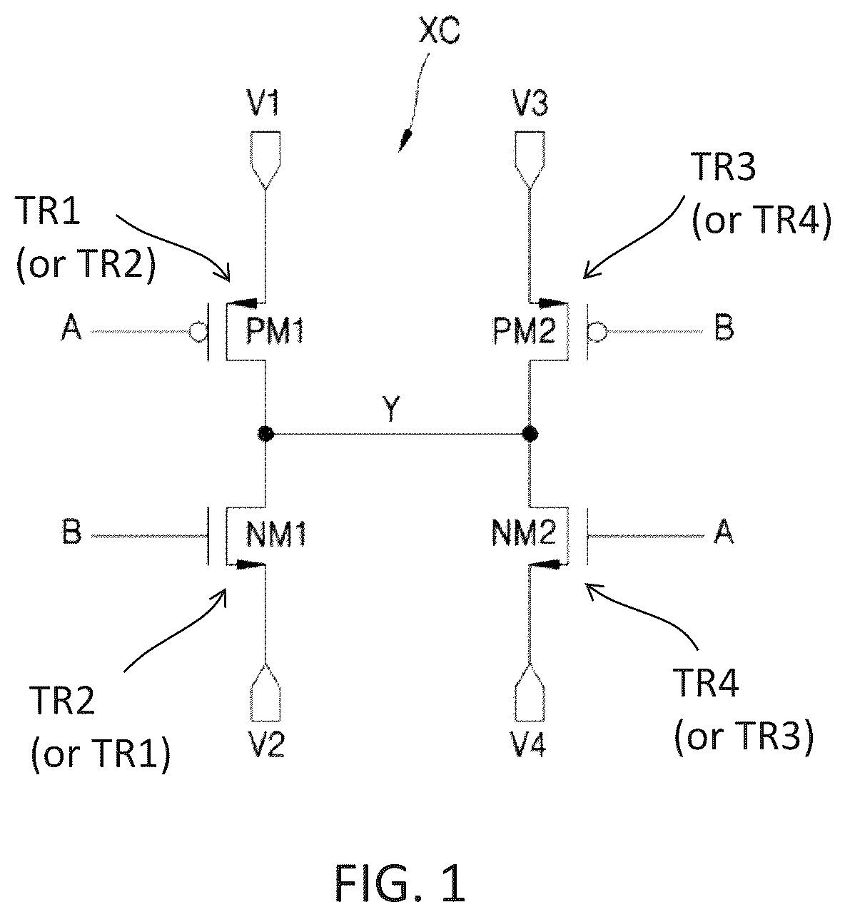
A cross-coupled structure may include stacked transistors. When those stacked transistors have a split gate structure that includes an insulating layer separating stacked gate structures from each other, methods of fabricating the cross-coupled structure may be complicated, and additional areas for wires may be required. According to some embodiments of the present invention, a cross-coupled structure may include a common gate structure including stacked gate structures that contact each other. is a circuit diagram of a cross-coupled structure XC according to some embodiments of the present invention. Referring to , the cross-coupled structure XC may include a first PMOS transistor PM 1 and a first NMOS transistor NM 1 connected in series and may also include a second PMOS transistor PM 2 and a second NMOS transistor NM 2 connected in series. The cross-coupled structure XC may be a portion of various cells (e.g., standard cells) including sequential logic cells (e.g., a latch, a flip-flop, a MUX, a multiplexer, or an adder). The first PMOS transistor PM 1 may include a source connected to a first voltage terminal V 1 , a gate receiving a first control signal A, and a drain connected to an output node Y. The first NMOS transistor NM 1 may include a drain connected to the output node Y, a gate receiving a second control signal B, and a source connected to a second voltage terminal V 2 . The second PMOS transistor PM 2 may include a source connected to a third voltage terminal V 3 , a gate receiving the second control signal B, and a drain connected to the output node Y. The second NMOS transistor NM 2 may include a drain connected to the output node Y, a gate receiving the first control signal A, and a source connected to a fourth voltage terminal V 4 . In some embodiments, the gates of the first PMOS transistor PM 1 and the second NMOS transistor NM 2 are electrically connected to each other to receive the first control signal A, and the gates of the first NMOS transistor NM 1 and the second PMOS transistor PM 2 are electrically connected to each other to receive the second control signal B. As such, the first and second PMOS transistors PM 1 and PM 2 and the first and second NMOS transistors NM 1 and NM 2 form the cross-coupled structure XC. In some embodiments, the first PMOS transistor PM 1 , the first NMOS transistor NM 1 , the second PMOS transistor PM 2 , and the second NMOS transistor NM 2 may be referred to as a first transistor TR 1 , a second transistor TR 2 , a third transistor TR 3 , and a fourth transistor TR 4 , respectively, as described throughout the specification. In some embodiments, the first NMOS transistor NM 1 , the first PMOS transistor PM 1 , the second NMOS transistor NM 2 , and the second PMOS transistor PM 2 may be referred to as a first transistor TR 1 , a second transistor TR 2 , a third transistor TR 3 , and a fourth transistor TR 4 , respectively. The first and third transistors TR 1 and TR 3 may be closer to a substrate (e.g., a substrate 90 in ) than the second and fourth transistors TR 2 and TR 4 . Accordingly, each of the first and third transistors TR 1 and TR 3 may be referred to as a lower transistor, and each of the second and fourth transistors TR 2 and TR 4 may be referred to as an upper transistor. The lower transistors may be PMOS transistors, and the upper transistors may be NMOS transistors, as described throughout the specification. The present invention, however, is not limited thereto. In some embodiments, the lower transistors may be NMOS transistors, and the upper transistors may be PMOS transistors. is a layout of a cross-coupled structure 100 according to some embodiments of the present invention. are perspective views of the cross-coupled structure 100 according to some embodiments of the present invention. Each of shows a group of elements, rather than all elements, to simplify these drawings. are cross-sectional views of the cross-coupled structure 100 according to some embodiments of the present invention. Each of shows cross-sectional views taken along the lines A-A′, B-B′, and C-C′ in according to some embodiments of the present invention, and some elements (e.g., a first conductive wire 82 _ 1 ) are omitted from to simplify these drawings. Referring to through 5 , the cross-coupled structure 100 may include a first transistor TR 1 , a second transistor TR 2 , a third transistor TR 3 , and a fourth transistor TR 4 . The first transistor TR 1 , the second transistor TR 2 , and the fourth transistor TR 4 may be spaced apart from each other in a first direction D 1 , and the first transistor TR 1 , the third transistor TR 3 , and the fourth transistor TR 4 may be spaced apart from each other in the first direction D 1 . The second transistor TR 2 and the third transistor TR 3 may be between the first transistor TR 1 and the fourth transistor TR 4 . The third transistor TR 3 and the second transistor TR 2 may be stacked in a second direction D 2 . The first direction D 1 may be different from the second direction D 2 . In some embodiments, the first direction D 1 may be perpendicular to the second direction D 2 . The cross-coupled structure 100 may also include a first dummy transistor DTR 1 and a second dummy transistor DTR 2 . The first transistor TR 1 and the first dummy transistor DTR 1 may be stacked in the second direction D 2 , and the second dummy transistor DTR 2 and the fourth transistor TR 4 may be stacked in the second direction D 2 . The first transistor TR 1 may include a first channel layer 12 _ 1 , a first gate electrode 16 _ 1 , a first source/drain region 32 _ 1 and a second source/drain region 32 _ 2 . The first channel layer 12 _ 1 may contact the first and second source/drain regions 32 _ 1 and 32 _ 2 and may include a portion that is in the first gate electrode 16 _ 1 . The first dummy transistor DTR 1 may include a first dummy channel layer 12 d _ 1 , a first dummy gate electrode 16 d _ 1 , a third source/drain region 32 _ 3 and a fourth source/drain region 32 _ 4 . The first dummy channel layer 12 d _ 1 may contact the third and fourth source/drain regions 32 _ 3 and 32 _ 4 and may include a portion that is in the first dummy gate electrode 16 d _ 1 . The third and fourth source/drain regions 32 _ 3 and 32 _ 4 may be spaced apart from the first and second source/drain regions 32 _ 1 and 32 _ 2 in the second direction D 2 . The second transistor TR 2 may include a second channel layer 12 _ 2 and a second gate electrode 16 _ 2 . A portion of the second channel layer 12 _ 2 may be in the second gate electrode 16 _ 2 . The third transistor TR 3 may include a third channel layer 12 _ 3 and a third gate electrode 16 _ 3 . A portion of the third channel layer 12 _ 3 may be in the third gate electrode 16 _ 3 . The second dummy transistor DTR 2 may include a second dummy channel layer 12 d _ 2 , a second dummy gate electrode 16 d _ 2 , a fifth source/drain region 32 _ 5 and a sixth source/drain region 32 _ 6 . The second dummy channel layer 12 d _ 2 may contact the fifth and sixth source/drain regions 32 _ 5 and 32 _ 6 and may include a portion that is in the second dummy gate electrode 16 d _ 2 . The first dummy transistor DTR 1 and the second dummy transistor DTR 2 may not be used as transistors that function as transistors. For example, each of the first dummy transistor DTR 1 and the second dummy transistor DTR 2 may not be turned on or turned off in response to voltages applied to nodes thereof. The fourth transistor TR 4 may include a fourth channel layer 12 _ 4 , a fourth gate electrode 16 _ 4 , a seventh source/drain region 32 _ 7 and an eight source/drain region 32 _ 8 . The fourth channel layer 12 _ 4 may contact the seventh and eight source/drain regions 32 _ 7 and 32 _ 8 and may include a portion that is in the fourth gate electrode 16 _ 4 . The second channel layer 12 _ 2 may contact the fourth source/drain region 32 _ 4 and the seventh source/drain region 32 _ 7 , and the fourth source/drain region 32 _ 4 and the seventh source/drain region 32 _ 7 may be source/drain regions of the second transistor TR 2 . The third channel layer 12 _ 3 may contact the second source/drain region 32 _ 2 and the fifth source/drain region 32 _ 5 , and the second source/drain region 32 _ 2 and the fifth source/drain region 32 _ 5 may be source/drain regions of the third transistor TR 3 . Referring to , a distance between a center of the first gate electrode 16 _ 1 in the first direction D 1 and a center of the second gate electrode 16 _ 2 in the first direction D 1 may be one critical poly pitch or contacted poly pitch (CPP). A distance between the center of the second gate electrode 16 _ 2 in the first direction D 1 and a center of the fourth gate electrode 16 _ 4 in the first direction D 1 may also be one CPP. Further, a distance between centers of two adjacent source/drain regions (e.g., the first and second source/drain regions 32 _ 1 and 32 _ 2 ) in the first direction D 1 may be one CPP. The cross-coupled structure 100 may be designed in an area corresponding to three CPP (3CPP), and the cross-coupled structure 100 may be referred to as a “3CPP cross-coupled structure.” The cross-coupled structure 100 may further include a first conductive wire 82 _ 1 electrically connected to both the first gate electrode 16 _ 1 and the fourth gate electrode 16 _ 4 . The first conductive wire 82 _ 1 may be electrically connected to each of the first gate electrode 16 _ 1 and the fourth gate electrode 16 _ 4 through a first vertical contact 52 _ 1 and a first via contact 62 _ 1 . The cross-coupled structure 100 may further include a fourth conductive wire 82 _ 4 electrically connected to the second gate electrode 16 _ 2 and the third gate electrode 16 _ 3 . The fourth conductive wire 82 _ 4 may be electrically connected to the second gate electrode 16 _ 2 through a fourth vertical contact 52 _ 4 and a fourth via contact 62 _ 4 . In some embodiments, the first vertical contacts 52 _ 1 may contact the first dummy gate electrode 16 d _ 1 and the fourth gate electrode 16 _ 4 , respectively, and the fourth vertical contact 52 _ 4 may contact the second gate electrode 16 _ 2 . The first conductive wire 82 _ 1 and the fourth conductive wire 82 _ 4 may be spaced apart from each other in a third direction D 3 . The third direction D 3 may be different from both the first and second directions D 1 and D 2 . In some embodiments, the third direction D 3 may be perpendicular to both the first and second directions D 1 and D 2 . Each of the first conductive wire 82 _ 1 and the fourth conductive wire 82 _ 4 may extend in the first direction D 1 as illustrated in . As used herein, “an element A extending in a direction X” (or similar language) may mean that the element A extends longitudinally in the direction X. In some embodiments, the first gate electrode 16 _ 1 and the third gate electrode 16 _ 3 may be spaced apart from each other in the first direction D 1 by a first distance dl, and the third gate electrode 16 _ 3 and the second dummy gate electrode 16 d _ 2 may be spaced apart from each other in the first direction D 1 by the first distance dl as illustrated in . The first gate electrode 16 _ 1 and the first dummy gate electrode 16 d _ 1 may contact each other and may be stacked in the second direction D 2 . The third gate electrode 16 _ 3 and the second gate electrode 16 _ 2 may contact each other and may be stacked in the second direction D 2 . The second dummy gate electrode 16 d _ 2 and the fourth gate electrode 16 _ 4 may contact each other and may be stacked in the second direction D 2 . Each of third, fourth, fifth and sixth source/drain regions 32 _ 3 , 32 _ 4 , 32 _ 5 and 32 _ 6 may include a first surface (e.g., 32 _ 3 S 1 , 32 _ 4 S 1 , 32 _ 5 S 1 and 32 _ 6 S 1 ) and a second surface (e.g., 32 _ 3 S 2 , 32 _ 4 S 2 , 32 _ 5 S 2 and 32 _ 6 S 2 ) that is opposite the first surface and is spaced apart from the first surface in the third direction D 3 . The cross-coupled structure 100 may further include a first conductive contact structure 42 C_ 1 and a second conductive contact structure 42 C_ 2 . The first conductive contact structure 42 C_ 1 may contact the first surfaces 32 _ 3 S 1 and 32 _ 4 S 1 of the third and fourth source/drain regions 32 _ 3 and 32 _ 4 , and the third and fourth source/drain regions 32 _ 3 and 32 _ 4 may be electrically connected to each other through the first conductive contact structure 42 C_ 1 . The second conductive contact structure 42 C_ 2 may contact the first surfaces 32 _ 5 S 1 and 32 _ 6 S 1 of the fifth and sixth source/drain regions 32 _ 5 and 32 _ 6 , and the fifth and sixth source/drain regions 32 _ 5 and 32 _ 6 may be electrically connected to each other through the second conductive contact structure 42 C_ 2 . Referring to , the first conductive contact structure 42 C_ 1 may overlap the third and fourth source/drain regions 32 _ 3 and 32 _ 4 in the third direction D 3 , and the second conductive contact structure 42 C_ 2 may overlap the fifth and sixth source/drain regions 32 _ 5 and 32 _ 6 in the third direction D 3 . As used herein, “an element A overlapping an element B in a direction W” (or similar language) may mean that at least one line extending in the direction W can be drawn that intersects both elements A and B. Referring to , the first, second, third and fourth transistors TR 1 , TR 2 , TR 3 and TR 4 , and the first and second dummy transistors DTR 1 and DTR 2 may be provided on a substrate 90 . The substrate 90 may include an upper surface 90 _U facing the first, second, third and fourth transistors TR 1 , TR 2 , TR 3 and TR 4 , and a lower surface 90 _L that is opposite the upper surface 90 _U of the substrate 90 . The first direction D 1 and the third direction D 3 may be parallel to the upper surface 90 _U of the substrate 90 , and the second direction D 2 may be perpendicular to the upper surface 90 _U of the substrate 90 . A first insulating layer 92 and a second insulating layer 94 may be provided on the substrate 90 . The first transistor TR 1 , the third transistor TR 3 and the second dummy transistor DTR 2 may include a first gate insulating layer 15 _ 1 , a third gate insulating layer 15 _ 3 , and a second dummy gate insulating layer 15 d _ 2 , respectively, and a first gate work function layer 17 _ 1 , a third gate work function layer 17 _ 3 , and a second dummy gate work function layer 17 d _ 2 , respectively. The first dummy transistor DTR 1 , the second transistor TR 2 and the fourth transistor TR 4 may include a first dummy gate insulating layer 15 d _ 1 , a second gate insulating layer 15 _ 2 , and a fourth gate insulating layer 15 _ 4 , respectively, and a first dummy gate work function layer 17 d _ 1 , a second gate work function layer 17 _ 2 , and a fourth gate work function layer 17 _ 4 . In some embodiments, the first gate electrode 16 _ 1 and the first dummy gate electrode 16 d _ 1 may include the same layer (e.g., the same metal layer), and an interface between the first gate electrode 16 _ 1 and the first dummy gate electrode 16 d _ 1 may not be visible. The first gate electrode 16 _ 1 , the first gate work function layer 17 _ 1 and the first dummy gate electrode 16 d _ 1 may collectively function as a gate structure of the first transistor TR 1 and thus may be collectively a first gate structure. The second dummy gate electrode 16 d _ 2 and the fourth gate electrode 16 _ 4 may include the same layer (e.g., the same metal layer), and an interface between the second dummy gate electrode 16 d _ 2 and the fourth gate electrode 16 _ 4 may not be visible. The fourth gate electrode 16 _ 4 , the fourth gate work function layer 17 _ 4 and the second dummy gate electrode 16 d _ 2 may collectively function as a gate structure of the fourth transistor TR 4 and thus may be collectively a fourth gate structure. The second transistor TR 2 and the third transistor TR 3 may include a second gate insulating layer 15 _ 2 and a third gate insulating layer 15 _ 3 , respectively, and a second work function layer 17 _ 2 and a third work function layer 17 _ 3 , respectively. The second gate electrode 16 _ 2 and the second work function layer 17 _ 2 may collectively function as a gate structure of a second transistor TR 2 and thus may be collectively a second gate structure. The third gate electrode 16 _ 3 and the third work function layer 17 _ 3 may collectively function as a gate structure of the third transistor TR 3 and thus may be collectively a third gate structure. The second and third gate structures may contact each other as illustrated in and may be a common gate structure. The common gate structure may include a first portion including the second gate electrode 16 _ 2 and the second work function layer 17 _ 2 and a second portion including the third gate electrode 16 _ 3 and the third work function layer 17 _ 3 . In some embodiments, the second gate electrode 16 _ 2 and the third gate electrode 16 _ 3 may include the same layer (e.g., the same metal layer), and an interface between the second gate electrode 16 _ 2 and the third gate electrode 16 _ 3 may not be visible. In some embodiments, the second gate electrode 16 _ 2 and the third gate electrode 16 _ 3 may include different layers (e.g., different metal layers). The first gate structure including the first gate electrode 16 _ 1 and the first dummy gate electrode 16 d _ 1 , the common gate structure including the second gate electrode 16 _ 2 and the third gate electrode 16 _ 3 , and the fourth gate structure including the fourth gate electrode 16 _ 4 and the second dummy gate electrode 16 d _ 2 may have a first thickness Tg in the second direction D 2 as illustrated in . The substrate 90 may include, for example, semiconductor material(s) (e.g., silicon, germanium, Silicon-germanium, and/or a Group III-V semiconductor compound). The substrate 90 may be a bulk substrate including only semiconductor material(s) or may include an insulating layer (e.g., a barrier insulating layer) on or below a semiconductor layer. Each of the channel layers (e.g., the first, second, third and fourth channel layers 12 _ 1 , 12 _ 2 , 12 _ 3 and 12 _ 4 and the first and second dummy channel layers 12 d _ 1 and 12 d _ 2 ) may include, for example, semiconductor material(s) (e.g., silicon, germanium, silicon-germanium, and/or a Group III-V semiconductor compound). Each of the channel layers may be, for example, a nanosheet. In some embodiments, the nanosheet may have a thickness in a range of from 1 nm to 100 nm (e.g., 5 nm to 10 nm) in the second direction D 2 . In some embodiments, each of the channel layers may be a fin-shaped channel layer or a nanowire. Each of the gate insulating layers (e.g., the first, second, third and fourth gate insulating layer 15 _ 1 , 15 _ 2 , 15 _ 3 and 15 _ 4 and the first and second dummy gate insulating layer 15 d _ 1 and 15 d _ 2 ) may include, for example, a silicon oxide layer and/or a high k dielectric layer including a high k material (e.g., hafnium silicate, zirconium silicate, hafnium dioxide and/or zirconium dioxide). Each of the source/drain regions (e.g., the first, second, third, fourth, fifth, sixth, seventh, and eight source/drain regions 32 _ 1 , 32 _ 2 , 32 _ 3 , 32 _ 4 , 32 _ 5 , 32 _ 6 , 32 _ 7 and 32 _ 8 ) may include, for example, semiconductor material(s) (e.g., silicon, germanium and silicon-germanium). Each of the first, second, fifth and sixth source/drain regions 32 _ 1 , 32 _ 2 , 32 _ 5 and 32 _ 6 may include impurities having a P type conductivity (e.g., boron (B), (Ga), aluminum (Al) and/or indium (In)), and each of the third, fourth, seventh and eight source/drain regions 32 _ 3 , 32 _ 4 , 32 _ 7 and 32 _ 8 may include impurities having an N type conductivity (e.g., phosphorus (P), arsenic (As), and/or antimony (Sb)). Each of the first conductive contact structure 42 C_ 1 and the second conductive contact structure 42 C_ 2 may include, for example, semiconductor material(s) (e.g., silicon, germanium, silicon-germanium, and/or a Group III-V semiconductor compound) and may additionally include impurities. In some embodiments, each of the first conductive contact structure 42 C_ 1 and the second conductive contact structure 42 C_ 2 may include a metallic layer including metal(s) (e.g., tungsten (W), aluminum (Al) and/or copper (Cu)). Each of the first and third work function layers 17 _ 1 and 17 _ 3 and the second dummy gate work function layer 17 d _ 2 may include a p-type work function layer (e.g., TiN layer). Each of the second and fourth work function layers 17 _ 2 and 17 _ 4 and the first dummy gate work function layer 17 d _ 1 may include an n-type work function layer (e.g., TiC layer, TiAl layer and/or TiAlC layer). Each of the gate electrodes (e.g., the first, second, third, fourth gate electrodes 16 _ 1 , 16 _ 2 , 16 _ 3 and 16 _ 4 and first and second dummy gate electrode 16 d _ 1 and 16 d _ 2 ) may include, for example, tungsten (W), aluminum (Al) and/or copper (Cu). Each of the first and second insulating layers 92 and 94 may include, for example, silicon oxide, silicon nitride, silicon oxynitride, silicon carbide and/or a low k material. Referring to , the first, second, third and fourth gate structures are similar to those illustrated in with a primary difference being that the first gate electrode 16 _ 1 and the first dummy gate electrode 16 d _ 1 may include different materials (e.g., different metal layers) as represented by different patterns, and the fourth gate electrode 16 _ 4 and the second dummy gate electrode 16 d _ 2 may include different materials (e.g., different metal layers) as represented by different patterns. Although illustrate that each of the transistors (i.e., the first, second, third and fourth transistors TR 1 , TR 2 , TR 3 and TR 4 , and the first and second dummy transistors DTR 1 and DTR 2 ) include three channel layers stacked in the second direction D 2 , the present invention is not limited thereto. In some embodiments, each of the transistors may include a single channel layer, two channel layers stacked in the second direction D 2 or four or more channel layers stacked in the second direction D 2 . is a layout of a cross-coupled structure 200 according to some embodiments of the present invention. is a perspective view of the cross-coupled structure 200 according to some embodiments of the present invention. shows a group of elements, rather than all elements, to simplify this drawing. The cross-coupled structure 200 is similar to the cross-coupled structure 100 with a primary difference being that the third and fourth source/drain regions 32 _ 3 and 32 _ 4 are electrically connected to each other through a second conductive wire 82 _ 2 and the fifth and sixth source/drain regions 32 _ 5 and 32 _ 6 are electrically connected to each other through a second gate wire 72 _ 2 . Each of the second conductive wire 82 _ 2 and the second gate wire 72 _ 2 may extend in the first direction D 1 . Referring to , each of the third and fourth source/drain regions 32 _ 3 and 32 _ 4 may contact a first gate wire 72 _ 1 , and each of the first gate wires 72 _ 1 may contact a second via contact 62 _ 2 , and the second via contacts 62 _ 2 may contact the second conductive wire 82 _ 2 . The cross-coupled structure 200 may further include a first lateral contact 42 _ 1 and a second lateral contact 42 _ 2 that may contact the first surfaces (e.g., the first surfaces 32 _ 5 S 1 and 32 _ 6 S 1 in ) of the fifth and sixth source/drain regions 32 _ 5 and 32 _ 6 , respectively. Each of the first and second lateral contacts 42 _ 1 and 42 _ 2 may contact a third vertical contact 52 _ 3 , and the third vertical contacts 52 _ 3 may contact the second gate wire 72 _ 2 . Each of the first gate wire 72 _ 1 , the second gate wire 72 _ 2 , the third vertical contact 52 _ 3 , and first and second lateral contacts 42 _ 1 and 42 _ 2 may include semiconductor material(s) (e.g., silicon, germanium, silicon-germanium, and/or a Group III-V semiconductor compound) and/or metallic material(s) (e.g., W, Al and/or Cu). Each of the second via contacts 62 _ 2 and the second conductive wire 82 _ 2 may include metallic material(s) (e.g., W, Al and/or Cu). is a layout of a cross-coupled structure 300 according to some embodiments of the present invention. is a perspective view of the cross-coupled structure 300 according to some embodiments of the present invention. shows a group of elements, rather than all elements, to simplify this drawing. The cross-coupled structure 300 is similar to the cross-coupled structure 100 with a primary difference being that the third and fourth source/drain regions 32 _ 3 and 32 _ 4 are electrically connected to each other through a second conductive wire 82 _ 2 . The cross-coupled structure 300 may further include a second conductive contact structure 42 C_ 2 that may contact the first surfaces (e.g., the first surfaces 32 _ 5 S 1 and 32 _ 6 S 1 in ) of the fifth and sixth source/drain regions 32 _ 5 and 32 _ 6 . is a layout of a cross-coupled structure 400 according to some embodiments of the present invention. is a perspective view of the cross-coupled structure 400 according to some embodiments of the present invention. shows a group of elements, rather than all elements, to simplify this drawing. The cross-coupled structure 400 is similar to the cross-coupled structure 200 with a primary difference being that the fifth and sixth source/drain regions 32 _ 5 and 32 _ 6 are electrically connected to each other through a third conductive wire 82 _ 3 . Each of the third vertical contacts 52 _ 3 may contact a third via contact 62 _ 3 , and the third via contacts 62 _ 3 may contact the third conductive wire 82 _ 3 . Each of the third via contact 62 _ 3 and the third conductive wire 82 _ 3 may include metallic material(s) (e.g., W, Al and/or Cu). The cross-coupled structure 400 may further include a first lateral contact 42 _ 1 and a second lateral contact 42 _ 2 that may contact the first surfaces (e.g., the first surfaces 32 _ 5 S 1 and 32 _ 6 S 1 in ) of the fifth and sixth source/drain regions 32 _ 5 and 32 _ 6 , respectively. Each of the first and second lateral contacts 42 _ 1 and 42 _ 2 may contact a third vertical contact 52 _ 3 , and the third vertical contacts 52 _ 3 may contact the third via contacts 62 _ 3 , respectively. Example embodiments are described herein with reference to the accompanying drawings. Many different forms and embodiments are possible without deviating from the scope of the present invention. Accordingly, the present invention should not be construed as limited to the example embodiments set forth herein. Rather, these example embodiments are provided so that this disclosure will be thorough and complete and will convey the scope of the present invention to those skilled in the art. In the drawings, the sizes and relative sizes of layers and regions may be exaggerated for clarity. Like reference numbers refer to like elements throughout. Example embodiments of the present invention are described herein with reference to cross-sectional views that are schematic illustrations of idealized embodiments and intermediate structures of example embodiments. As such, variations from the shapes of the illustrations as a result, for example, of manufacturing techniques and/or tolerances, are to be expected. Thus, example embodiments of the present invention should not be construed as limited to the particular shapes illustrated herein but include deviations in shapes that result, for example, from manufacturing, unless the context clearly indicates otherwise. Unless otherwise defined, all terms (including technical and scientific terms) used herein have the same meaning as commonly understood by one of ordinary skill in the art to which the present invention belongs. It will be further understood that terms, such as those defined in commonly used dictionaries, should be interpreted as having a meaning that is consistent with their meaning in the context of the relevant art and will not be interpreted in an idealized or overly formal sense unless expressly so defined herein. The terminology used herein is for the purpose of describing particular embodiments only and is not intended to be limiting of the present invention. As used herein, the singular forms “a,” “an” and “the” are intended to include the plural forms as well, unless the context clearly indicates otherwise. It will be further understood that the terms “comprises,” “comprising,” “includes” and/or “including,” when used in this specification, specify the presence of the stated features, steps, operations, elements and/or components, but do not preclude the presence or addition of one or more other features, steps, operations, elements, components and/or groups thereof. As used herein the term “and/or” includes any and all combinations of one or more of the associated listed items. It will be understood that although the terms first, second, etc. may be used herein to describe various elements, these elements should not be limited by these terms. These terms are only used to distinguish one element from another. Thus, a first element could be termed a second element without departing from the scope of the present invention. The above-disclosed subject matter is to be considered illustrative, and not restrictive, and the appended claims are intended to cover all such modifications, enhancements, and other embodiments, which fall within the scope of the invention. Thus, to the maximum extent allowed by law, the scope is to be determined by the broadest permissible interpretation of the following claims and their equivalents and shall not be restricted or limited by the foregoing detailed description.
Figures (12)
Citations
This patent cites (19)
- US9472558
- US10163915
- US10297592
- US10840146
- US10971504
- US11004856
- US2006/0220134
- US2017/0133380
- US2018/0108646
- US2019/0131309
- US2019/0288004
- US2019/0386011
- US2020/0104460
- US2020/0321355
- US2021/0043630
- US2021/0098500
- US2021/0111028
- US2021/0118799
- US202114158