Abstract
A semiconductor device includes a substrate having at least one active region, the at least one active region being defined by an isolation layer, at least one word line extending in a first horizontal direction inside the substrate, the at least one word line crossing the at least one active region, at least one bit line extending in a second horizontal direction orthogonal to the first horizontal direction, the at least one bit line being at a higher vertical level than the at least one word line, and at least one direct contact electrically connecting the at least one bit line to the at least one active region, the at least one direct contact having a maximum width in a third horizontal direction, the third horizontal direction intersecting each of the first horizontal direction and the second horizontal direction at an acute angle.
Claims (20)
1 . A semiconductor device, comprising: a substrate having at least one active region, the at least one active region being defined by an isolation layer; at least one word line extending in a first horizontal direction inside the substrate, the at least one word line crossing the at least one active region; at least one bit line extending in a second horizontal direction orthogonal to the first horizontal direction, the at least one bit line being at a higher vertical level than the at least one word line; and at least one direct contact electrically connecting the at least one bit line to the at least one active region, the at least one direct contact having a maximum width in a third horizontal direction, the third horizontal direction intersecting each of the first horizontal direction and the second horizontal direction at an acute angle.
10 . A semiconductor device, comprising: a substrate; an isolation layer defining an active region in the substrate; a word line crossing the active region in a first horizontal direction, the word line dividing the active region into a first impurity region and a second impurity region; a bit line extending on the substrate in a second horizontal direction orthogonal to the first horizontal direction; and a direct contact electrically connecting the bit line to the first impurity region, the direct contact having a long axis extending in a third horizontal direction intersecting with the first horizontal direction and the second horizontal direction, and a shape of the direct contact includes a first curve and a second curve that meet on the long axis.
16 . A semiconductor device, comprising: a substrate; an isolation layer in the substrate; active regions defined by the isolation layer, each of the active regions including a first impurity region and second impurity regions, the second impurity regions being separated from each other by the first impurity region; word lines extending in a first horizontal direction inside the substrate, each of the word lines crossing between the first impurity region and one of the second impurity regions; bit lines extending in a second horizontal direction orthogonal to the first horizontal direction, the bit lines being at a higher vertical level than the word lines; and direct contacts electrically connecting the bit lines to the first impurity regions, each of the direct contacts having a maximum width in a third horizontal direction intersecting with each of the first horizontal direction and the second horizontal direction at an acute angle, wherein the first impurity region has a maximum width in the third horizontal direction.
Show 17 dependent claims
2 . The semiconductor device as claimed in claim 1 , wherein the at least one direct contact has an oval shape having a long axis extending in the third horizontal direction.
3 . The semiconductor device as claimed in claim 1 , wherein the at least one direct contact has a long axis extending in the third horizontal direction, a shape of the at least one direct contact including a first curve and a second curve recessed with respect to the long axis.
4 . The semiconductor device as claimed in claim 3 , wherein the first curve and the second curve meet on the long axis with a cusp.
5 . The semiconductor device as claimed in claim 3 , wherein the shape of the at least one direct contact further includes a third curve and a fourth curve recessed with respect to the long axis.
6 . The semiconductor device as claimed in claim 1 , wherein: the third horizontal direction makes a first angle with the first horizontal direction, and the at least one active region extends in a fourth horizontal direction intersecting at an acute angle with each of the first horizontal direction and the second horizontal direction, the fourth horizontal direction making a second angle greater than the first angle with the first horizontal direction.
7 . The semiconductor device as claimed in claim 1 , wherein: the at least one active region includes a first impurity region and second impurity regions, the second impurity regions being separated from each other by the first impurity region, and the at least one direct contact is electrically connected to the first impurity region, the first impurity region having a maximum width in the third horizontal direction.
8 . The semiconductor device as claimed in claim 1 , further comprising an extra pad on the at least one active region, the extra pad being electrically connected to the at least one active region.
9 . The semiconductor device as claimed in claim 1 , further comprising an additional direct contact separated from the at least one direct contact in a diagonal direction intersecting with the first horizontal direction and the second horizontal direction at an acute angle.
11 . The semiconductor device as claimed in claim 10 , wherein the shape of the direct contact is an oval shape.
12 . The semiconductor device as claimed in claim 10 , wherein the first curve and the second curve are recessed with respect to the long axis.
13 . The semiconductor device as claimed in claim 10 , wherein the first curve and the second curve have a cusp on the long axis.
14 . The semiconductor device as claimed in claim 10 , wherein the shape of the direct contact further includes a third curve and a fourth curve, the first to fourth curves being recessed with respect to the long axis.
15 . The semiconductor device as claimed in claim 14 , wherein the first curve and the second curve, the second curve and the third curve, the third curve and the fourth curve, and the fourth curve and the first curve meet with a cusp, respectively.
17 . The semiconductor device as claimed in claim 16 , wherein each of the direct contacts has an oval shape having a long axis extending in the third horizontal direction.
18 . The semiconductor device as claimed in claim 16 , wherein the active regions extend in a fourth horizontal direction intersecting at an acute angle with the first horizontal direction and the second horizontal direction.
19 . The semiconductor device as claimed in claim 18 , wherein the third horizontal direction makes a first angle with the first horizontal direction, and the fourth horizontal direction makes a second angle greater than the first angle with the first horizontal direction.
20 . The semiconductor device as claimed in claim 16 , wherein the direct contacts are separated from each other in a diagonal direction intersecting with the first horizontal direction and the second horizontal direction at an acute angle.
Full Description
Show full text →
CROSS-REFERENCE TO RELATED APPLICATION
This application is based on and claims priority under 35 U.S.C. § 119 to Korean Patent Application No. 10-2022-0116631, filed on Sep. 15, 2022, in the Korean Intellectual Property Office, the disclosure of which is incorporated by reference herein in its entirety.
BACKGROUND
1. Field Embodiments relate to a semiconductor device, and more particularly, to a semiconductor device including a direct contact. 2. Description of the Related Art Along with the rapid development of the electronics industry and the demands of users, electronic devices have been gradually made small and lightweight. Therefore, because a semiconductor device having a high degree of integration to be used for electronic devices is demanded, the design rules for components of a semiconductor device have decreased. Accordingly, the difficulty of a manufacturing process of increasing a contact area between conductive patterns constituting a semiconductor device has gradually increased.
SUMMARY
According to an aspect of embodiments, there is provided a semiconductor device including a substrate having an active region defined by an isolation layer, a word line extending in a first horizontal direction inside the substrate and crossing the active region, a bit line extending in a second horizontal direction orthogonal to the first horizontal direction at a higher vertical level than the word line, and a plurality of direct contacts electrically connecting the bit line to the active region, wherein each of the plurality of direct contacts has a maximum width in a third horizontal direction intersecting at an acute angle with each of the first horizontal direction and the second horizontal direction. According to another aspect of embodiments, there is provided a semiconductor device including a substrate, an isolation layer defining an active region in the substrate, a word line dividing the active region into a first impurity region and a second impurity region while crossing the active region in a first horizontal direction, a bit line extending on the substrate in a second horizontal direction orthogonal to the first horizontal direction, and a direct contact electrically connecting the bit line to the first impurity region, wherein the direct contact has a long axis extending in a third horizontal direction intersecting with the first horizontal direction and the second horizontal direction and has a shape including a first curve and a second curve, which meet on the long axis. According to another aspect of embodiments, there is provided a semiconductor device including a substrate, an isolation layer in the substrate, an active region including a first impurity region and second impurity regions separated from each other with the first impurity region therebetween, and defined by the isolation layer, a word line extending in a first horizontal direction inside the substrate and crossing between the first impurity region and second impurity region, a bit line extending in a second horizontal direction orthogonal to the first horizontal direction at a higher vertical level than the word line, and a plurality of direct contacts electrically connecting the bit line to the first impurity region, wherein the direct contact has a maximum width in a third horizontal direction intersecting at an acute angle with each of the first horizontal direction and the second horizontal direction, and the first impurity region has a maximum width in the third horizontal direction.
BRIEF DESCRIPTION OF THE DRAWINGS
Features will become apparent to those of skill in the art by describing in detail exemplary embodiments with reference to the attached drawings, in which: A is a layout diagram illustrating main components of a semiconductor device according to embodiments; B is a cross-sectional view taken along line I-I′ of A to describe the semiconductor device according to embodiments; A is an enlarged layout diagram illustrating some components of the semiconductor device of A according to embodiments; B is a magnified top view of a region EX 1 of A ; A and 3 B are magnified top views illustrating some components of semiconductor devices according to embodiments; A is a layout diagram illustrating main components of a semiconductor device according to some embodiments; B is a cross-sectional view taken along line II-II′ of A to describe the semiconductor device according to some embodiments; A to 13 B are top views and cross-sectional views of stages in a method of manufacturing a semiconductor device, according to embodiments; and is a block diagram illustrating a system including a semiconductor device according to embodiments.
DETAILED DESCRIPTION
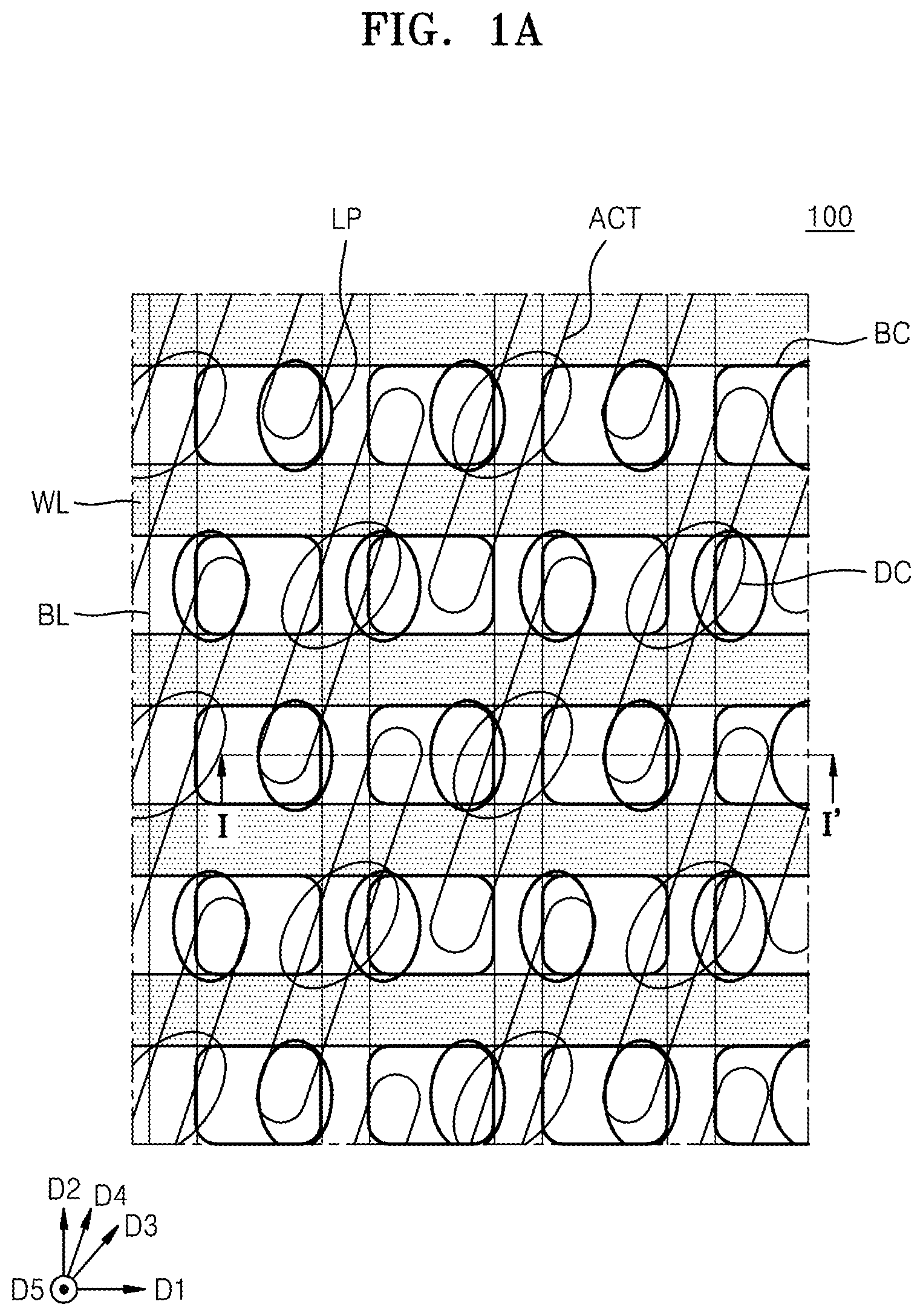
A is a layout diagram illustrating main components of a semiconductor device 100 according to embodiments. B is a cross-sectional view taken along line I-I′ of A . Referring to A , the semiconductor device 100 may include a plurality of active regions ACT horizontally extending in a diagonal direction with respect to a first horizontal direction D 1 and a second horizontal direction D 2 in a top view. In some embodiments, the plurality of active regions ACT may extend in a fourth horizontal direction D 4 . It is noted that hereinafter a “horizontal direction” refers to a direction parallel to a top surface of a substrate, and an element that extends horizontally in “a diagonal direction” extends in parallel to the top surface of the substrate while extending at an oblique angle with respect to any of the edges of the substrate. A “vertical” direction or level refers to a direction or distance along a direction normal or perpendicular to the top surface of the substrate. A plurality of word lines WL may extend in parallel to each other in the first horizontal direction D 1 and cross the plurality of active regions ACT. Above the plurality of word lines WL, a plurality of bit lines BL may extend in parallel to each other in the second horizontal direction D 2 intersecting with the first horizontal direction D 1 . The plurality of bit lines BL may be connected to the plurality of active regions ACT via a plurality of direct contacts DC. In some embodiments, a plurality of buried contacts BC may be formed between two adjacent bit lines BL among the plurality of bit lines BL. Each of the plurality of buried contacts BC may extend to a top of any one of the two adjacent bit lines BL. In some embodiments, the plurality of buried contacts BC may be arranged in a line in the first horizontal direction D 1 and the second horizontal direction D 2 . A plurality of landing pads LP may be respectively formed on the plurality of buried contacts BC. The plurality of buried contacts BC and the plurality of landing pads LP may connect lower electrodes of capacitors formed on the plurality of bit lines BL to the plurality of active regions ACT. The plurality of landing pads LP may partially overlap the plurality of buried contacts BC, respectively. A more detailed description of the semiconductor device 100 is made below. Referring to B , the semiconductor device 100 may include a substrate 101 in which the plurality of active regions ACT are defined by an isolation layer 112 . The substrate 101 may be a wafer including silicon (Si). Alternatively, the substrate 101 may be a wafer including a semiconductor element, e.g., germanium (Ge), or a compound semiconductor, e.g., silicon carbide (SiC), gallium arsenide (GaAs), indium arsenide (InAs), or indium phosphide (InP). In addition, the substrate 101 may have a silicon on insulator (SOI) structure. In addition, the substrate 101 may include a conductive region, e.g., an impurity-doped well or an impurity-doped structure. The isolation layer 112 may be formed in a first trench T 1 formed in the substrate 101 . The isolation layer 112 may include, e.g., silicon oxide, silicon nitride, or a combination thereof. In the substrate 101 , the active region ACT may be defined by the isolation layer 112 . The active region ACT may be arranged in a bar shape extending in a diagonal direction with respect to the first horizontal direction D 1 and the second horizontal direction D 2 . In detail, the active region ACT may extend in the fourth horizontal direction D 4 intersecting, e.g., at an oblique angle, with the first horizontal direction D 1 and the second horizontal direction D 2 . The active region ACT may include a first impurity region SD 1 and second impurity regions SD 2 separated from each other with the first impurity region SD 1 therebetween, e.g., the first impurity region SD 1 may be between two second impurity regions SD 2 within a same active region ACT. A channel region may be formed between the first impurity region SD 1 and each of the second impurity regions SD 2 . In the substrate 101 , the plurality of word lines WL described above with reference to A may be buried. A buffer layer 122 may be formed on the substrate 101 . The buffer layer 122 may cover an upper surface of the isolation layer 112 . For example, the buffer layer 122 may include a stacked structure of first silicon oxide, silicon nitride, and second silicon oxide sequentially formed on the substrate 101 . The plurality of bit lines BL extending in parallel to each other in the second horizontal direction D 2 may be on the buffer layer 122 . The plurality of bit lines BL may be separated from each other in the first horizontal direction D 1 . The direct contact DC may be on a partial region of each of the plurality of active regions ACT. Particularly, the direct contact DC may be on the first impurity region SD 1 of each of the plurality of active regions ACT. Each of the plurality of bit lines BL may be connected to the active region ACT via the direct contact DC. The direct contact DC may include, e.g., tungsten (W), tungsten nitride (WN), cobalt (Co), nickel (Ni), aluminum (Al), molybdenum (Mo), ruthenium (Ru), titanium (Ti), titanium nitride (TiN), tantalum (Ta), tantalum nitride (TaN), copper (Cu), or a combination thereof. In some embodiments, the direct contact DC may include doped polysilicon. The direct contact DC will be described in more detail below. In some embodiments, a lower conductive layer 130 may include doped polysilicon. Each of an intermediate conductive layer 132 and an upper conductive layer 134 may include a layer including Ti, TiN, titanium silicon nitride (TiSiN), W, WN, tungsten silicide (WSi), tungsten silicon nitride (WSiN), Ru, or a combination thereof. For example, the intermediate conductive layer 132 may include a TiN layer and/or a TiSiN layer, and the upper conductive layer 134 may include a layer including Ti, TiN, W, WN, WSiN, Ru, or a combination thereof. An insulating capping pattern 136 may include silicon nitride. For example, as illustrated in B , the lower conductive layer 130 , the intermediate conductive layer 132 , and the upper conductive layer 134 may be stacked on top of each other to constitute each of the plurality of bit lines BL. In a partial region of the substrate 101 , a plurality of recess spaces R 1 may be formed in the active region ACT. The plurality of recess spaces R 1 may be filled with a plurality of contact plugs 150 , respectively. Each of the plurality of contact plugs 150 may have a pillar shape extending in a vertical direction D 5 from the recess space R 1 . Each of the plurality of contact plugs 150 may be in contact with the active region ACT. A lower end portion of each of the plurality of contact plugs 150 may be at a lower level than an upper surface of the substrate 101 so as to be buried in the substrate 101 . The plurality of contact plugs 150 may include, e.g., a metal only, a metal and a metal silicide layer, or doped polysilicon. The plurality of contact plugs 150 may be arranged in a line in the second horizontal direction D 2 between a pair of bit lines BL selected from among the plurality of bit lines BL and adjacent to each other. An insulating fence may be between every two of the plurality of contact plugs 150 arranged in a line in the second horizontal direction D 2 . The plurality of contact plugs 150 may be insulated from each other by the insulating fence. For example, the insulating fence may include silicon nitride. The insulating fence may have a pillar shape extending on the substrate 101 in the vertical direction D 5 . A plurality of metal silicide layers 152 and the plurality of landing pads LP may be on the plurality of contact plugs 150 , respectively. Each of the plurality of landing pads LP may extend lengthwise in the vertical direction D 5 above the contact plug 150 . Each of the plurality of landing pads LP may be electrically connected to the contact plug 150 via the metal silicide layer 152 . Each of the plurality of landing pads LP may include a conductive barrier layer 154 and a metal layer 156 . In some embodiments, the conductive barrier layer 154 may include Ti, TiN, or a combination thereof, and the metal layer 156 may include W. The plurality of landing pads LP may have a pattern shape of a plurality of islands in a top view. In some embodiments, the metal silicide layer 152 may include, e.g., cobalt silicide, nickel silicide, or manganese silicide. In some embodiments, the metal silicide layer 152 may be omitted. The contact plug 150 and the metal silicide layer 152 may constitute the buried contact BC. The contact plug 150 , the metal silicide layer 152 , and the landing pad LP sequentially disposed on the substrate 101 may constitute a contact structure electrically connected to the active region ACT at a position adjacent to the bit line BL in the first horizontal direction D 1 . Both, e.g., opposite, side walls of each of the plurality of bit lines BL and a plurality of insulating capping patterns 136 respectively covering upper surfaces of the plurality of bit lines BL may be covered by a spacer structure SP. One spacer structure SP may be between one bit line BL selected from among the plurality of bit lines BL and the plurality of contact plugs 150 arranged in a line in the second horizontal direction D 2 at a position adjacent to the one bit line BL. Each of a plurality of spacer structures SP may include an inner spacer 142 , an intermediate spacer 146 , and an outer spacer 148 . The inner spacer 142 may be in contact with each of a side wall of the bit line BL and a side wall of the direct contact DC. The inner spacer 142 may include a part in contact with the contact plug 150 . The inner spacer 142 may include, e.g., silicon nitride. The intermediate spacer 146 may be between the inner spacer 142 and the outer spacer 148 in the first horizontal direction D 1 . The intermediate spacer 146 may have a side wall facing the bit line BL with the inner spacer 142 therebetween and a side wall facing the contact plug 150 , the metal silicide layer 152 , and the landing pad LP with the outer spacer 148 therebetween. The intermediate spacer 146 may include, e.g., silicon oxide, an air spacer, or a combination thereof. The outer spacer 148 may be in contact with a side wall of each of the contact plug 150 , the metal silicide layer 152 , and the landing pad LP. The outer spacer 148 may be separated from the inner spacer 142 with the intermediate spacer 146 therebetween. In some embodiments, the outer spacer 148 may include, e.g., silicon nitride. The spacer structure SP may extend in parallel to the bit line BL in the second horizontal direction D 2 . The insulating capping pattern 136 and the spacer structure SP may constitute an insulating structure covering an upper surface and both side walls of the bit line BL. A gap-fill pattern 144 may be between the direct contact DC and the contact plug 150 . The gap-fill pattern 144 may be separated from the direct contact DC with the inner spacer 142 therebetween. The gap-fill pattern 144 may surround the direct contact DC by covering side walls of the direct contact DC. The gap-fill pattern 144 may be in contact with the inner spacer 142 and the contact plug 150 . In some embodiments, the gap-fill pattern 144 may include silicon nitride. A structure including the inner spacer 142 and the gap-fill pattern 144 may be referred to as an insulating pattern IP. Although not shown in B , a plurality of capacitors may respectively be on the plurality of landing pads LP. The plurality of capacitors may include a plurality of lower electrodes, a capacitor dielectric layer, and an upper electrode. The capacitor dielectric layer may cover the plurality of lower electrodes. The upper electrode may cover the capacitor dielectric layer and face the plurality of lower electrodes with the capacitor dielectric layer therebetween. A is an enlarged layout diagram illustrating some components of the semiconductor device 100 according to embodiments. B is a magnified top view of a region EX 1 of A . A and 2 B show only some components for convenience of description. Referring to A , the plurality of word lines WL may extend in the first horizontal direction D 1 and cross the plurality of active regions ACT. The active region ACT may include the first impurity region SD 1 (e.g., in a center the active region ACT) and the second impurity regions SD 2 (e.g., at edges of the active region ACT) separated from each other with the first impurity region SD 1 therebetween. The word line WL may divide the active region ACT into the first impurity region SD 1 and the second impurity region SD 2 , e.g., two word lines WL may intersect each active region ACT. The first impurity region SD 1 and the second impurity region SD 2 may be separated from each other with the word line WL therebetween. The direct contact DC may be electrically connected to the first impurity region SD 1 . Particularly, the direct contact DC may be on the first impurity region SD 1 of each of the plurality of active regions ACT. That is, each of the plurality of bit lines BL may be connected to the first impurity region SD 1 via the direct contact DC. In some embodiments, the direct contact DC may have a shape long in a third horizontal direction D 3 , e.g., the direct contact DC may extend lengthwise in the third horizontal direction D 3 . That is, the direct contact DC may have a maximum width L in the third horizontal direction D 3 , e.g., the direct contact DC may have its longest dimension in the third horizontal direction D 3 . In some embodiments, a plurality of direct contacts DC may be separated from each other in a diagonal direction intersecting with the first horizontal direction D 1 and the second horizontal direction D 2 . For example, the plurality of direct contacts DC may be separated from each other in the third horizontal direction D 3 , e.g., a direction at an oblique or acute angle with respect to each of the first and second directions D 1 and D 2 . As another example, the plurality of direct contacts DC may be separated from each other in the fourth horizontal direction D 4 . As yet another example, the plurality of direct contacts DC may be separated from each other in another diagonal direction intersecting with the third horizontal direction D 3 and the fourth horizontal direction D 4 . Referring to B , in some embodiments, the third horizontal direction D 3 in which the direct contact DC has a maximum width may be different from the fourth horizontal direction D 4 in which the active region ACT extends, e.g., longitudinal directions of the direct contact DC and the active region ACT may be different from each other. In detail, when each of the third horizontal direction D 3 and the fourth horizontal direction D 4 intersect at an acute angle with the first horizontal direction D 1 and the second horizontal direction D 2 , the third horizontal direction D 3 may intersect at a smaller angle with the first horizontal direction D 1 than the fourth horizontal direction D 4 intersects with the first horizontal direction D 1 . For example, as illustrated in B , the third horizontal direction D 3 may intersect at a first angle θ1 with the first horizontal direction D 1 , and the fourth horizontal direction D 4 may be intersect at a second angle θ2 greater than the first angle θ1 with the first horizontal direction D 1 . In some embodiments, the third horizontal direction D 3 (in which the direct contact DC has a maximum width) may be a direction in which the first impurity region SD 1 has a maximum width. In detail, the first impurity region SD 1 defined by the word line WL may have a shape inclined in the fourth horizontal direction D 4 like the active region ACT and have a maximum width in a horizontal direction intersecting with the fourth horizontal direction D 4 . For example, when the first impurity region SD 1 has a shape substantially close to a parallelogram, the first impurity region SD 1 may have a maximum width in a diagonal direction, and the diagonal direction may be the third horizontal direction D 3 in which the direct contact DC has a maximum width. For example, referring to B , while the entirety of the active region ACT is inclined at the second angle θ2 with respect to the first horizontal direction D 1 (i.e., in the fourth horizontal direction D 4 ), both the direct contact DC and the first impurity region SD 1 may have shapes with maximum widths inclined at the first angle θ1 with the first horizontal direction D 1 (i.e., in the third horizontal direction D 3 ). For example, as further illustrated in B , since both the direct contact DC and the first impurity region SD 1 have maximum widths in a same direction, e.g., a direction at an oblique angle with respect to edges of the substrate 101 , an overlap area between the direct contact DC and the first impurity region SD 1 may increase, e.g., the direct contact DC may completely cover and overlap the first impurity region SD 1 . In some embodiments, unlike B , a direction in which the first impurity region SD 1 has a maximum width may be different from a direction in which the direct contact DC has a maximum width. For example, the direction in which the first impurity region SD 1 has a maximum width may intersect at a less angle with the first horizontal direction D 1 than the third horizontal direction D 3 . As another example, the direction in which the first impurity region SD 1 has a maximum width may intersect at a greater angle with the first horizontal direction D 1 than the third horizontal direction D 3 . In some embodiments, the direct contact DC may be arranged to have a maximum width in the third horizontal direction D 3 intersecting with the first horizontal direction D 1 and the second horizontal direction D 2 . For example, the direct contact DC may have an oval shape having a long axis extending in the third horizontal direction D 3 , as viewed in a top view. A and 3 B are magnified top views illustrating some components of semiconductor devices 100 a and 100 b according to embodiments. Referring to A , the direct contact DC may have a shape having a long axis extending in the third horizontal direction D 3 and including a first curve CL 1 and a second curve CL 2 recessed with respect to the long axis. In some embodiments, the direct contact DC may include the first curve CL 1 and the second curve CL 2 intersecting with each other at two points, and the two points of intersection may be two points on the long axis extending in the third horizontal direction D 3 . That is, a distance between the two points of intersection may be a maximum value among distances between random two points on the first curve CL 1 and the second curve CL 2 . In some embodiments, the first curve CL 1 and the second curve CL 2 may meet each other on the long axis with cusps. That is, the direct contact DC may not have a full oval shape but a shape distorted with two vertices. Referring to B , the direct contact DC may have a shape having a long axis extending in the third horizontal direction D 3 and including first to fourth curves CL 1 , CL 2 , CL 3 , and CL 4 recessed with respect to the long axis. In some embodiments, the direct contact DC may have a shape including the first to fourth curves CL 1 , CL 2 , CL 3 , and CL 4 intersecting with each other, and two points of intersection having a maximum distance therebetween among four points of intersection may be two points on the long axis extending in the third horizontal direction D 3 . That is, the maximum distance between the two points of intersection may be a maximum value among distances between random two points on the first to fourth curves CL 1 , CL 2 , CL 3 , and CL 4 . In some embodiments, the first curve CL 1 and the second curve CL 2 , the second curve CL 2 and the third curve CL 3 , the third curve CL 3 and the fourth curve CL 4 , and the fourth curve CL 4 and the first curve CL 1 may meet with a cusp, respectively. That is, the direct contact DC may not have a full oval shape but a shape distorted with four vertices. In some embodiments, the direct contact DC may have a similar shape to a parallelogram including four sides recessed with respect to a center of the parallelogram. A is a layout diagram illustrating main components of a semiconductor device 200 according to some embodiments. B is a cross-sectional view taken along line II-II′ of A . Referring to A and 4 B , the semiconductor device 200 having an extra pad 210 is provided. Hereinafter, differences relative to the semiconductor device 100 described with reference to A and 1 B are mainly described. The plurality of active regions ACT may be arranged in a bar shape extending in the fourth horizontal direction D 4 intersecting with the first horizontal direction D 1 and the second horizontal direction D 2 . For example, as illustrated in A and 4 B , the extra pad 210 may have a greater horizontal width (e.g., in the first horizontal direction D 1 ) than the active region ACT, and may be on each of the plurality of active regions ACT. In another example, the extra pad 210 may have a horizontal width not greater than that of the active region ACT. In some embodiments, one direct contact DC and a pair of contact plugs 150 facing each other with the one direct contact DC therebetween may be electrically connected to different active regions ACT among the plurality of active regions ACT, respectively. That is, the contact plug 150 may be directly connected to the extra pad 210 by forming a contact surface therebetween, the extra pad 210 having a greater horizontal width than the active region ACT. The contact plug 150 and the metal silicide layer 152 may constitute the buried contact BC. The contact plug 150 , the metal silicide layer 152 , and the landing pad LP sequentially disposed on the substrate 101 may constitute a contact structure electrically connected to the active region ACT via the extra pad 210 at a position adjacent to the bit line BL in the first horizontal direction D 1 . In some embodiments, a level of the lowest surface of the contact plug 150 may be higher than a level of the lowest surface of the extra pad 210 and lower than a level of the highest surface of the extra pad 210 . In addition, the level of the lowest surface of the contact plug 150 may be higher than a level of the highest surface of the active region ACT and lower than a level of the highest surface of the isolation layer 112 . That is, the contact plug 150 may be electrically connected to the active region ACT via the extra pad 210 without being in direct contact with the active region ACT. For example, the extra pad 210 may include a single-layer structure of doped polysilicon. In this case, the plurality of contact plugs 150 may be fully made of doped polysilicon. In another example, the extra pad 210 may include a single-layer structure of a metal. In this case, the plurality of contact plugs 150 may be fully made of a metal. In some embodiments, unlike A and 4 B , the extra pad 210 may have a stacked structure of a lower pad including doped polysilicon and an upper pad including a metal. Herein, the contact plug 150 may include a metal of substantially the same material as that of the upper pad. In some embodiments, the contact plug 150 may be in direct contact with the upper pad, and in this case, the contact plug 150 and the upper pad include the same material, and thus a contact resistance between the contact plug 150 and the upper pad may be very low. In some embodiments, the extra pad 210 may further include a metal silicide layer between the lower pad and the upper pad. In addition, the contact plug 150 may further include a metal silicide layer along a contact surface with the upper pad. In some embodiments, unlike A and 4 B , the extra pad 210 may have a less horizontal width than the active region ACT. In this case, the semiconductor device 200 may include the extra pad 210 disposed on the active region ACT and having a less horizontal width than the active region ACT, and an additional spacer formed on both side walls of the extra pad 210 . According to embodiments, the semiconductor device 100 (or 200 ) including the direct contact DC having a maximum width in the third horizontal direction D 3 may be provided. In embodiments, by arranging the direct contact DC so as to have a maximum width in the third horizontal direction D 3 , a contact area between the direct contact DC and the first impurity region SD 1 may increase. In embodiments, by arranging the direct contact DC so as to have a maximum width in the third horizontal direction D 3 , an electrical connection between the bit line BL and the active region ACT may be improved. Accordingly, a semiconductor device with improved performance and reliability may be provided. A to 13 B are top views and cross-sectional views of stages in a method of manufacturing the semiconductor device 100 , according to embodiments. In detail, A, 6 A, 7 A, 8 A, 9 A, 10 A, 11 A, 12 A, and 13 A are top views showing only some components according to a process order to describe the method of manufacturing the semiconductor device 100 . B, 6 B, 7 B, 8 B, 9 B, 10 B, 11 B, 12 B, and 13 B are cross-sectional views taken along line of A, 6 A, 7 A, 8 A, 9 A, 10 A, 11 A, 12 A, and 13 A , respectively, to describe the method of manufacturing the semiconductor device 100 . Referring to A and 5 B , the isolation layer 112 may be formed on the substrate 101 . The active region ACT may be defined by the isolation layer 112 . An impurity injection process may be performed on the active region ACT to form the first impurity region SD 1 and a pair of second impurity regions SD 2 on each active region ACT. The pair of second impurity regions SD 2 may be separated from each other in a horizontal direction with the first impurity region SD 1 therebetween. The first and second impurity regions SD 1 and SD 2 may be doped to have the same conductivity type (e.g., N type). An insulating layer 113 and a polysilicon layer 114 may be formed on the substrate 101 . The insulating layer 113 may include a plurality of insulating layers. The insulating layer 113 may include a silicon oxide layer, a silicon nitride layer, or a combination thereof. The polysilicon layer 114 may include a doped polysilicon layer. The insulating layer 113 may include the buffer layer 122 of B . On the polysilicon layer 114 , a target mask layer TM, a first insulating layer ILL a first mask layer ML 1 , a second insulating layer IL 2 , a second mask layer ML 2 , a third insulating layer IL 3 , a third mask layer ML 3 , and a fourth insulating layer IL 4 may be sequentially formed. For example, as illustrated in B , a stack of alternating mask layers and insulating layers may be formed on the polysilicon layer 114 . The target mask layer TM may include a spin on hardmask (SOH) layer. The target mask layer TM may further include a silicon oxide layer beneath the SOH layer. The first insulating layer IL 1 may include a silicon nitride layer and/or a silicon oxynitride layer. The first mask layer ML 1 may include an SOH layer. The second insulating layer IL 2 may include a silicon nitride layer and/or a silicon oxynitride layer. The second mask layer ML 2 may include an SOH layer. The third insulating layer IL 3 may include a silicon nitride layer and/or a silicon oxynitride layer. The third mask layer ML 3 may include an SOH layer. The fourth insulating layer IL 4 may include a silicon nitride layer and/or a silicon oxynitride layer. A first photoresist layer PR 1 may be formed on the fourth insulating layer IL 4 . The first photoresist layer PR 1 may be patterned using a first photomask. Referring to A and 6 B , a first opening OP 1 may be formed by patterning the fourth insulating layer IL 4 and the third mask layer ML 3 . The first opening OP 1 may extend in a horizontal direction parallel to the upper surface of the substrate 101 . For example, the first opening OP 1 may extend in the first horizontal direction D 1 like the word line WL. As another example, the first opening OP 1 may extend in the second horizontal direction D 2 . That is, the first opening OP 1 may extend in a direction intersecting with the word line WL. In the specification, although the first horizontal direction D 1 or the second horizontal direction D 2 is described as a direction in which the first opening OP 1 is patterned, this is only illustrative, and the first opening OP 1 may be patterned in another horizontal direction. Forming the first opening OP 1 may include patterning the fourth insulating layer IL 4 and the third mask layer ML 3 by using the patterned first photoresist layer PR 1 on the fourth insulating layer IL 4 , as an etching mask. The first photoresist layer PR 1 remaining thereafter may be removed. A first insulating film IF 1 may be conformally formed above a front, e.g., upper, surface of the substrate 101 . The first insulating film IF 1 may be formed on exposed side surfaces of the fourth insulating layer IL 4 and the third mask layer ML 3 . The first insulating film IF 1 may define the first opening OP 1 together with the third insulating layer IL 3 , e.g., a width of the first opening OP 1 between facing surfaces of the first insulating film IF 1 in the second horizontal direction D 2 may be L 1 . The third insulating layer IL 3 may be exposed by the first opening OP 1 . The first insulating film IF 1 may include a silicon oxide layer. The first insulating film IF 1 may be formed by atomic layer deposition (ALD). After forming the first insulating film IF 1 , a first etch-back process may be performed. By the first etch-back process, a portion of the first insulating film IF 1 on the fourth insulating layer IL 4 and a portion of the first insulating film IF 1 on the third insulating layer IL 3 may be removed. Referring to A and 7 B , a second opening OP 2 may be formed by patterning the third insulating layer IL 3 and the second mask layer ML 2 . The second opening OP 2 may extend in a direction parallel to the first opening OP 1 . That is, the second opening OP 2 may extend in a horizontal direction parallel to the upper surface of the substrate 101 . For example, the second opening OP 2 may extend in the first horizontal direction D 1 like the word line WL. As another example, the second opening OP 2 may extend in the second horizontal direction D 2 . That is, the second opening OP 2 may extend in a direction intersecting with the word line WL. In embodiments, like the first opening OP 1 , the second opening OP 2 may be patterned in a horizontal direction that is different from the first horizontal direction D 1 and the second horizontal direction D 2 and parallel to the first opening OP 1 . In some embodiments, a width of the second opening OP 2 may be less than a half of a width of the first opening OP 1 . In some embodiments, the width of the second opening OP 2 may be about one third of the width of the first opening OP 1 . For example, referring to A- 7 B , when the first opening OP 1 and the second opening OP 2 extend in the first horizontal direction D 1 , a width of the first opening OP 1 in the second horizontal direction D 2 may be L 1 (see A ), and a width of the second opening OP 2 in the second horizontal direction D 2 may be L 2 . In other words, the width L 2 of the second opening OP 2 in the second horizontal direction D 2 may be about one third of the width L 1 of the first opening OP 1 in the second horizontal direction D 2 . Forming the second opening OP 2 may include removing the fourth insulating layer IL 4 and the third mask layer ML 3 by using the first insulating film IF 1 on the third insulating layer IL 3 , as an etching mask, and patterning the third insulating layer IL 3 and the second mask layer ML 2 . Thereafter, the first insulating film IF 1 may be removed. A second insulating film IF 2 may be conformally formed above the front surface of the substrate 101 . The second insulating film IF 2 may be formed on exposed side surfaces of the third insulating layer IL 3 and the second mask layer ML 2 . The second insulating film IF 2 may define the second opening OP 2 together with the second insulating layer IL 2 . The second insulating layer IL 2 may be exposed by the second opening OP 2 . The second insulating film IF 2 may include a silicon oxide layer. The second insulating film IF 2 may be formed by ALD. After forming the second insulating film IF 2 , a second etch-back process may be performed. By the second etch-back process, a portion of the second insulating film IF 2 on the third insulating layer IL 3 and a portion of the second insulating film IF 2 on the second insulating layer IL 2 may be removed. Referring to A and 8 B , a third opening OP 3 may be formed by patterning the first insulating layer IL 1 . The third opening OP 3 may extend in a direction parallel to the second opening OP 2 and the first opening OP 1 . That is, the third opening OP 3 may extend in a horizontal direction parallel to the upper surface of the substrate 101 . For example, the third opening OP 3 may extend in the first horizontal direction D 1 like the word line WL. As another example, the third opening OP 3 may extend in the second horizontal direction D 2 . That is, the third opening OP 3 may extend in a direction intersecting with the word line WL. In embodiments, like the first opening OP 1 and the second opening OP 2 , the third opening OP 3 may be patterned in a horizontal direction that is different from the first horizontal direction D 1 and the second horizontal direction D 2 and parallel to the first opening OP 1 and the second opening OP 2 . The target mask layer TM may be exposed by the third opening OP 3 . In some embodiments, a width of the third opening OP 3 may be substantially the same as the width of the second opening OP 2 . In some embodiments, the width of the third opening OP 3 may be about one third of the width of the first opening OP 1 . For example, when the first opening OP 1 , the second opening OP 2 , and the third opening OP 3 extend in the first horizontal direction D 1 , a width of the third opening OP 3 in the second horizontal direction D 2 may be L 3 . In other words, the width L 3 of the third opening OP 3 in the second horizontal direction D 2 may be substantially the same as the width L 2 of the second opening OP 2 in the second horizontal direction D 2 and about one third of the width L 1 of the first opening OP 1 in the second horizontal direction D 2 . Forming the third opening OP 3 may include removing the third insulating layer IL 3 and the second mask layer ML 2 by using the second insulating film IF 2 on the second insulating layer IL 2 , as an etching mask, and patterning the second insulating layer IL 2 and the first mask layer ML 1 . The first insulating layer IL 1 may be patterned by using the second insulating layer IL 2 and the first mask layer ML 1 as an etching mask. In some embodiments, processes of patterning the second insulating layer IL 2 , the first mask layer ML 1 , and the first insulating layer IL 1 may be simultaneously performed. Alternatively, the processes of patterning the second insulating layer IL 2 , the first mask layer ML 1 , and the first insulating layer IL 1 may be sequentially performed. Thereafter, the second insulating layer IL 2 and the first mask layer ML 1 may be removed. Referring to 9 A and 9 B, a fourth mask layer ML 4 , a fifth insulating layer IL 5 , a fifth mask layer ML 5 , and a sixth insulating layer IL 6 may be sequentially formed on the target mask layer TM. The fourth mask layer ML 4 may cover the patterned first insulating layer IL 1 . The fourth mask layer ML 4 may fill the third openings OP 3 . Although the first insulating layer IL 1 and the third opening OP 3 are not shown in A due to being covered by the fourth mask layer ML 4 , the first insulating layer IL 1 and the third opening OP 3 are indicated by dashed lines in A for convenience of description. The fourth mask layer ML 4 may include an SOH layer. The fifth insulating layer IL 5 may include a silicon nitride layer and/or a silicon oxynitride layer. The fifth mask layer ML 5 may include an SOH layer. The sixth insulating layer IL 6 may include a silicon nitride layer and/or a silicon oxynitride layer. A second photoresist layer PR 2 may be formed on the sixth insulating layer IL 6 . The second photoresist layer PR 2 may be patterned using a second photomask. The patterned second photoresist layer PR 2 may extend in a diagonal direction intersecting with the first horizontal direction D 1 and the second horizontal direction D 2 . The patterned second photoresist layer PR 2 may extend in a sixth horizontal direction D 6 , as illustrated in A . The sixth horizontal direction D 6 may be selected so that the plurality of direct contacts DC have a long axis in the third horizontal direction D 3 , as described with reference to A . The sixth horizontal direction D 6 may be the diagonal direction of A in which the plurality of direct contacts DC are separated from each other. Referring to A and 10 B , a fourth opening OP 4 may be formed by patterning the sixth insulating layer IL 6 and the fifth mask layer ML 5 . The fourth opening OP 4 may extend in a horizontal direction parallel to the upper surface of the substrate 101 . For example, the fourth opening OP 4 may extend in the sixth horizontal direction D 6 . Although the first insulating layer IL 1 and the third opening OP 3 are not shown by being covered by the fifth insulating layer IL 5 and the fourth mask layer ML 4 , the first insulating layer IL 1 and the third opening OP 3 are indicated by dashed lines in A , for convenience of description. Forming the fourth opening OP 4 may include patterning the sixth insulating layer IL 6 and the fifth mask layer ML 5 by using the patterned second photoresist layer PR 2 on the sixth insulating layer IL 6 , as an etching mask. The second photoresist layer PR 2 remaining thereafter may be removed. A third insulating film IF 3 may be conformally formed above the front surface of the substrate 101 . The third insulating film IF 3 may be formed on exposed side surfaces of the sixth insulating layer IL 6 and the fifth mask layer ML 5 . The third insulating film IF 3 may define the fourth opening OP 4 together with the fifth insulating layer IL 5 . The fifth insulating layer IL 5 may be exposed by the fourth opening OP 4 . The third insulating film IF 3 may include a silicon oxide layer. The third insulating film IF 3 may be formed by ALD. After forming the third insulating film IF 3 , a third etch-back process may be performed. By the third etch-back process, a portion of the third insulating film IF 3 on the sixth insulating layer IL 6 and a portion of the third insulating film IF 2 on the fifth insulating layer IL 5 may be removed. Referring to A and 11 B , the fifth insulating layer IL 5 may be patterned. Patterning the fifth insulating layer IL 5 may include removing the sixth insulating layer IL 6 and the fifth mask layer ML 5 by using the third insulating film IF 3 on the fifth insulating layer IL 5 , as an etching mask, and patterning the fifth insulating layer IL 5 . In some embodiments, processes of patterning the sixth insulating layer IL 6 , the fifth mask layer ML 5 , and the fifth insulating layer IL 5 may be simultaneously performed. Alternatively, the processes of patterning the sixth insulating layer IL 6 , the fifth mask layer ML 5 , and the fifth insulating layer IL 5 may be sequentially performed. Although the first insulating layer IL 1 and the third opening OP 3 are not shown by being covered by the fourth mask layer ML 4 , the first insulating layer IL 1 and the third opening OP 3 are indicated by dashed lines for convenience of description. Referring to A and 12 B , a fifth opening OP 5 may be formed by patterning the fourth mask layer ML 4 . The fifth opening OP 5 may extend in a direction parallel to the fourth opening OP 4 . That is, the fifth opening OP 5 may extend in a horizontal direction parallel to the upper surface of the substrate 101 . For example, the fifth opening OP 5 may extend in the sixth horizontal direction D 6 . For convenience of description, a portion of the first insulating layer IL 1 , which is not shown by being covered by the fifth insulating layer IL 5 , is indicated by a dashed line. Forming the fifth opening OP 5 may include removing a portion of the fourth mask layer ML 4 by using the fifth insulating layer IL 5 on the fourth mask layer ML 4 , as an etching mask, thereby exposing the first insulating layer IL 1 through the fifth opening OP 5 . A portion of the fourth mask layer ML 4 may be further removed by using the exposed first insulating layer IL 1 as an etching mask. By further removing the portion of the fourth mask layer ML 4 , by using the exposed first insulating layer IL 1 as an etching mask, the third opening OP 3 may be exposed again. By exposing the third opening OP 3 , the target mask layer TM may be exposed. In some embodiments, the exposed target mask layer TM may have a parallelogram shape in a top view, as illustrated in A (e.g., dotted portions between layers IL 1 and IL 5 ). This may be because the first insulating layer IL 1 has been patterned in the first horizontal direction D 1 and the fifth insulating layer IL 5 has been patterned in the sixth horizontal direction D 6 that is a diagonal direction intersecting with the first horizontal direction D 1 . Referring to A and 13 B , a plurality of direct contact holes DCH may be formed by patterning the target mask layer TM. The active region ACT of the substrate 101 may be exposed through the direct contact hole DCH. In detail, the first impurity region SD 1 of the substrate 101 may be exposed through the direct contact hole DCH. Patterning the target mask layer TM may include patterning the target mask layer TM exposed through the fifth opening OP 5 and the third opening OP 3 . In detail, patterning the target mask layer TM may include patterning the target mask layer TM by using, as an etching mask, the fifth insulating layer IL 5 extending in the sixth horizontal direction D 6 and the first insulating layer IL 1 extending in the first horizontal direction D 1 , e.g., etching the exposed parallelogram shape of the target mask layer TM. As illustrated in A , unlike the parallelogram shape of the exposed target mask layer in A , a resultant etched shape of the direct contact hole DCH formed by patterning the target mask layer TM may not be a parallelogram with straight lines, but a shape close to a smoothed parallelogram, e.g., with curved lines. For example, due to the etching process, the resultant etched shape of the direct contact hole DCH may be closer to an oval or a distorted oval shape (e.g., a distorted oval shape with vertices illustrate in A and 3 B ). Specifically, etching may not be completely performed on a vertex of the parallelogram shape and a portion adjacent thereto. Accordingly, since etching is not performed on the portion, a direct contact hole having a smooth parallelogram shape may be formed. In some embodiments, the direct contact hole DCH may have a shape extending lengthwise (e.g., having a longitudinal direction) in the third horizontal direction D 3 . That is, the direct contact hole DCH may have a maximum width in the third horizontal direction D 3 . For example, the direct contact hole DCH may have an oval shape having a long axis extending in the third horizontal direction D 3 . For example, the direct contact hole DCH may have a shape having a long axis extending in the third horizontal direction D 3 and including the first curve CL 1 and the second curve CL 2 recessed with respect to the long axis ( A ). As another example, the direct contact hole DCH may have a shape having a long axis extending in the third horizontal direction D 3 and including the first to fourth curves CL 1 , CL 2 , CL 3 , and CL 4 recessed with respect to the long axis ( B ). That is, the direct contact hole DCH may have a shape formed by smoothing four vertices of a parallelogram. In some embodiments, the plurality of direct contact holes DCH may be separated from each other in the sixth horizontal direction D 6 . In some embodiments, the sixth horizontal direction D 6 intersecting at an acute angle with the first horizontal direction D 1 and the second horizontal direction D 2 may intersect at a greater angle with the first horizontal direction D 1 than the third horizontal direction D 3 . In some embodiments, unlike shown in A , the sixth horizontal direction D 6 may intersect at a smaller angle with the first horizontal direction D 1 than the third horizontal direction D 3 . In some embodiments, the sixth horizontal direction D 6 may be parallel to the third horizontal direction D 3 . A subsequent process of manufacturing the semiconductor device 100 would be obvious to those of ordinary skill in the art, and thus, a detailed description thereof is omitted herein. As shown in A, 1 B, and 5 A to 13 B , the semiconductor device 100 may include the direct contact DC, which may be formed by quadruple patterning and diagonal patterning, thereby reducing misalignment between direct contacts DC. Particularly, the plurality of direct contact holes DCH may be formed at one time, e.g., simultaneously, by patterning the target mask layer TM (see A ) by quadruple patterning and diagonal patterning, thereby reducing misalignment which may occur between the plurality of direct contact holes DCH. is a block diagram illustrating a system 1000 including a semiconductor device according to embodiments. Referring to , the system 1000 may include a controller 1010 , an input/output device 1020 , a memory 1030 , an interface 1040 , and a bus 1050 . The system 1000 may be a mobile system or a system for transmitting or receiving information. In some embodiments, the mobile system may be, e.g., a portable computer, a web tablet, a mobile phone, a digital music player, or a memory card. The controller 1010 may control an execution program in the system 1000 . For example, the controller 1010 may include a microprocessor, a digital signal processor, a microcontroller, or a similar device. The input/output device 1020 may be used for the system 1000 to input or output data. The system 1000 may use the input/output device 1020 to be connected to an external device, e.g., a personal computer or a network, and exchange data with the external device. The input/output device 1020 may include, e.g., a touch screen, a touch pad, a keyboard, or a display. The memory 1030 may store data for an operation of the controller 1010 or store data processed by the controller 1010 . The memory 1030 may include any one of the semiconductor devices 100 , 100 a , 100 b , and 200 according to embodiments. The interface 1040 may be a data transmission passage between the system 1000 and an external device. The controller 1010 , the input/output device 1020 , the memory 1030 , and the interface 1040 may communicate with each other via the bus 1050 . By way of summation and review, embodiments provide a semiconductor device with improved performance and reliability. That is, embodiments provide a semiconductor device having a direct contact (DC) which connects a bit line to an active region and has an elongated shape, e.g., an oval shape, extending in a diagonal direction with respect to edge of a substrate. The direct contact is formed to overlap, e.g., fully cover and extend beyond, an impurity region in a center of the active region, thereby increasing a contact area between the direct contact and the impurity region. In addition, the direct contact may be patterned one time, thereby reducing misalignment. Example embodiments have been disclosed herein, and although specific terms are employed, they are used and are to be interpreted in a generic and descriptive sense only and not for purpose of limitation. In some instances, as would be apparent to one of ordinary skill in the art as of the filing of the present application, features, characteristics, and/or elements described in connection with a particular embodiment may be used singly or in combination with features, characteristics, and/or elements described in connection with other embodiments unless otherwise specifically indicated. Accordingly, it will be understood by those of skill in the art that various changes in form and details may be made without departing from the spirit and scope of the present invention as set forth in the following claims.
Figures (20)
Citations
This patent cites (14)
- US8378499
- US9214382
- US9230612
- US10685963
- US11411010
- US2022/0037330
- US2023/0189504
- US111640749
- US10-2014-0028910
- US10-2015-0012943
- US10-2019-0131885
- US10-2059863
- US10-2021-0032843
- US10-2021-0158258