Semiconductor Device and Method of Fabricating the Same
Abstract
A semiconductor device including memory cells that are three-dimensionally arranged is provided. The semiconductor device includes: a stack structure including first and second layers, which are sequentially stacked on a substrate, the first layer including first and second semiconductor patterns, which are spaced apart from each other and extend in a first direction, and a first bitline, which extends in a second direction different from the first direction and is electrically connected to the first and second semiconductor patterns, the second layer including third and fourth semiconductor patterns, which are spaced apart from each other and extend in the first direction, and a second bitline, which extends in the second direction and is electrically connected to the third and fourth semiconductor patterns, and each of the first through fourth semiconductor patterns including a source, a channel, a drain, and a bottom electrode; a first wordline connecting the channels of the first and third semiconductor patterns in a vertical direction; a second wordline connecting the channels of the second and fourth semiconductor patterns in the vertical direction.
Claims (11)
1 . A semiconductor device comprising: a stack structure including first and second layers, which are sequentially stacked on a substrate, the first layer including first and second semiconductor patterns, which extend in a first direction and are spaced apart in a second direction different from the first direction, and a first bitline, which extends in the second direction and is electrically connected to the first and second semiconductor patterns, the second layer including third and fourth semiconductor patterns, which extend in the first direction and are spaced apart in the second direction, and a second bitline, which extends in the second direction and is electrically connected to the third and fourth semiconductor patterns, and each of the first through fourth semiconductor patterns including a source, a channel, a drain, and a bottom electrode; a first wordline connecting the channels of the first and third semiconductor patterns in a vertical direction, the first and third semiconductor patterns being spaced apart from each other in the vertical direction; and a second wordline connecting the channels of the second and fourth semiconductor patterns in the vertical direction, the second and fourth semiconductor patterns being spaced apart from each other in the vertical direction, wherein a first distance, in the first direction, between the first bitline and the first wordline differs from a second distance, in the first direction, between the first bitline and the second wordline, and the first wordline and the second wordline are spaced apart in the second direction.
10 . A semiconductor device comprising: a stack structure including first and second layers, which are sequentially stacked on a substrate, the first layer including first and second semiconductor patterns, which are spaced apart from each other and extend in a first direction, and a first bitline, which extends in a second direction different from the first direction and is electrically connected to the first and second semiconductor patterns, the second layer including third and fourth semiconductor patterns, which are spaced apart from each other and extend in the first direction, and a second bitline, which extends in the second direction and is electrically connected to the third and fourth semiconductor patterns, and each of the first through fourth semiconductor patterns including a source, a channel, a drain, and a bottom electrode; a first wordline connecting the channels of the first and third semiconductor patterns in a vertical direction; a second wordline connecting the channels of the second and fourth semiconductor patterns in the vertical direction; and a gate insulating film surrounding four sides of each of the channels of each of the first through fourth semiconductor patterns, on each of the first through fourth semiconductor patterns, wherein a first distance, in the first direction, between the first bitline and the first wordline differs from a second distance, in the first direction, between the first bitline and the second wordline.
11 . A semiconductor device comprising: a stack structure including first and second layers, which are sequentially stacked on a substrate, the first layer including first and second semiconductor patterns, which are spaced apart from each other and extend in a first direction, and a first bitline, which extends in a second direction different from the first direction and is electrically connected to the first and second semiconductor patterns, the second layer including third and fourth semiconductor patterns, which are spaced apart from each other and extend in the first direction, and a second bitline, which extends in the second direction and is electrically connected to the third and fourth semiconductor patterns, and each of the first through fourth semiconductor patterns including a source, a channel, a drain, and a bottom electrode; a first wordline connecting the channels of the first and third semiconductor patterns in a vertical direction; and a second wordline connecting the channels of the second and fourth semiconductor patterns in the vertical direction, wherein a first distance, in the first direction, between the first bitline and the first wordline differs from a second distance, in the first direction, between the first bitline and the second wordline, wherein the first and second layers are arranged in a stepwise shape so that the first bitline of the first layer includes an exposed region exposed by the second layer, and wherein the semiconductor device further comprises a bitline contact in contact with the exposed region of the first bitline.
Show 8 dependent claims
2 . The semiconductor device of claim 1 , further comprising: an isolation insulating film disposed between the first and second wordlines to extend in the vertical direction.
3 . The semiconductor device of claim 2 , wherein the isolation insulating film is in contact with the first and second wordlines and is self-aligned.
4 . The semiconductor device of claim 2 , further comprising: an intervening semiconductor pattern extending in the first direction between the first and second semiconductor patterns, wherein the isolation insulating film is formed to penetrate the intervening semiconductor pattern.
5 . The semiconductor device of claim 2 , wherein a width, in the first direction, of the isolation insulating film is greater than a width, in the first direction, of the first or second wordline.
6 . The semiconductor device of claim 1 , wherein is the source, the channel, and the drain of the first semiconductor pattern are positioned on a first side of the bottom electrode of the first semiconductor pattern, and the isolation insulating film is positioned on a second side of the bottom electrode of the first semiconductor pattern.
7 . The semiconductor device of claim 1 , wherein the first layer further includes a fifth semiconductor pattern, which extends in the first direction, the first, second, and fifth semiconductor patterns are sequentially arranged, the second layer further includes a sixth semiconductor pattern, which extends in the first direction, the third, fourth, and sixth semiconductor patterns are sequentially arranged, each of the fifth and sixth semiconductor patterns includes a source, a channel, a drain, and a bottom electrode, and the semiconductor device further comprises a third wordline connecting the channels of the fifth and sixth semiconductor patterns in the vertical direction.
8 . The semiconductor device of claim 7 , wherein an imaginary line connecting centers of the first and third wordlines does not overlap with the second wordline.
9 . The semiconductor device of claim 1 , wherein the first layer further includes a seventh semiconductor pattern, which extends in the first direction between the first and second semiconductor patterns, and a third bitline, which is electrically connected to the seventh semiconductor pattern, the first bitline is disposed on a first side of the first semiconductor pattern, and the third bitline is disposed on a second side of the seventh semiconductor pattern.
Full Description
Show full text →
CROSS-REFERENCE TO RELATED APPLICATION
This application claims priority from Korean Patent Application No. 10-2022-0143198 filed on Oct. 31, 2022 in the Korean Intellectual Property Office, and all the benefits accruing therefrom under 35 U.S.C. 119, the contents of which in its entirety are herein incorporated by reference.
BACKGROUND
1. Field The present disclosure relates to a semiconductor device and a method of fabricating the same. 2. Description of the Related Art In the degree of integration of semiconductor memory devices including memory cells that are two-dimensionally arranged, planar areas that unit memory cells occupy may be main factors for deciding the degree of integration. Therefore, the degree of integration of the semiconductor memory devices may be largely affected by the level of a technology for forming fine patterns. The degree of integration of the semiconductor memory devices can be raised using ultra high-priced equipment, but there still is a limit in increasing the degree of integration of the semiconductor memory devices. Accordingly, semiconductor devices including memory cells that are three-dimensionally arranged have been proposed.
SUMMARY
Aspects of the present disclosure provide a semiconductor device including memory cells that are three-dimensionally arranged. Aspects of the present disclosure also provide a method of fabricating a semiconductor device including memory cells that are three-dimensionally arranged. However, aspects of the present disclosure are not restricted to those set forth herein. The above and other aspects of the present disclosure will become more apparent to one of ordinary skill in the art to which the present disclosure pertains by referencing the detailed description of the present disclosure given below. According to an aspect of the present disclosure, a semiconductor device includes: a stack structure including first and second layers, which are sequentially stacked on a substrate, the first layer including first and second semiconductor patterns, which are spaced apart from each other and extend in a first direction, and a first bitline, which extends in a second direction different from the first direction and is electrically connected to the first and second semiconductor patterns, the second layer including third and fourth semiconductor patterns, which are spaced apart from each other and extend in the first direction, and a second bitline, which extends in the second direction and is electrically connected to the third and fourth semiconductor patterns, and each of the first through fourth semiconductor patterns including a source, a channel, a drain, and a bottom electrode; a first wordline connecting the channels of the first and third semiconductor patterns in a vertical direction; a second wordline connecting the channels of the second and fourth semiconductor patterns in the vertical direction, wherein a first distance, in the first direction, between the first bitline and the first wordline differs from a second distance, in the first direction, between the first bitline and the second wordline. According to another aspect of the present disclosure, a semiconductor device includes: a substrate including a capacitor region and first and second switching regions, which are disposed on both sides of the capacitor region; a stack structure including a plurality of layers, which are sequentially stacked on the substrate, each of the layers including a plurality of cell transistors, which are disposed in the first or second switching region and include first and second cell transistors, and a plurality of capacitors, which are disposed in the capacitor region and include first and second capacitors, the first cell transistor being electrically connected to the first capacitor and disposed in the first switching region, and the second cell transistor being electrically connected to the second capacitor and disposed in the second switching region; and a plurality of wordlines arranged vertically on the substrate and electrically connecting gates of the cell transistors. According to another aspect of the present disclosure, a semiconductor device includes: a stack structure including first and second layers, which are sequentially stacked on a substrate, the first layer including first, second, and third semiconductor patterns, which are spaced apart from one another and extend in a first direction, a first bitline, which extends in a second direction different from the first direction and is electrically connected to the first and third semiconductor patterns, and a second bitline, which is electrically connected to the second semiconductor pattern, the second layer including fourth, fifth, and sixth semiconductor patterns, which are spaced apart from one another and extend in the first direction, a third bitline, which extends in the second direction and is electrically connected to the fourth and sixth semiconductor patterns, and a fourth bitline, which is electrically connected to the fifth semiconductor pattern, and each of the first through sixth semiconductor patterns including a source, a channel, a drain, and a bottom electrode; a first wordline connecting the channels of the first and fourth semiconductor patterns in a vertical direction; a second wordline connecting the channels of the second and fifth semiconductor patterns in the vertical direction; a third wordline connecting the channels of the third and sixth semiconductor patterns in the vertical direction; and an isolation insulating film disposed to extend in the vertical direction between the first and third wordlines, the isolation insulating film being in contact with the first and second wordlines and being self-aligned. A first distance, in the first direction, between the first bitline and the first wordline differs from a second distance, in the first direction, between the first bitline and the third wordline, and the isolation insulating film is formed to penetrate the second and fifth semiconductor patterns. It should be noted that the effects of the present disclosure are not limited to those described above, and other effects of the present disclosure will be apparent from the following description.
BRIEF DESCRIPTION OF THE DRAWINGS
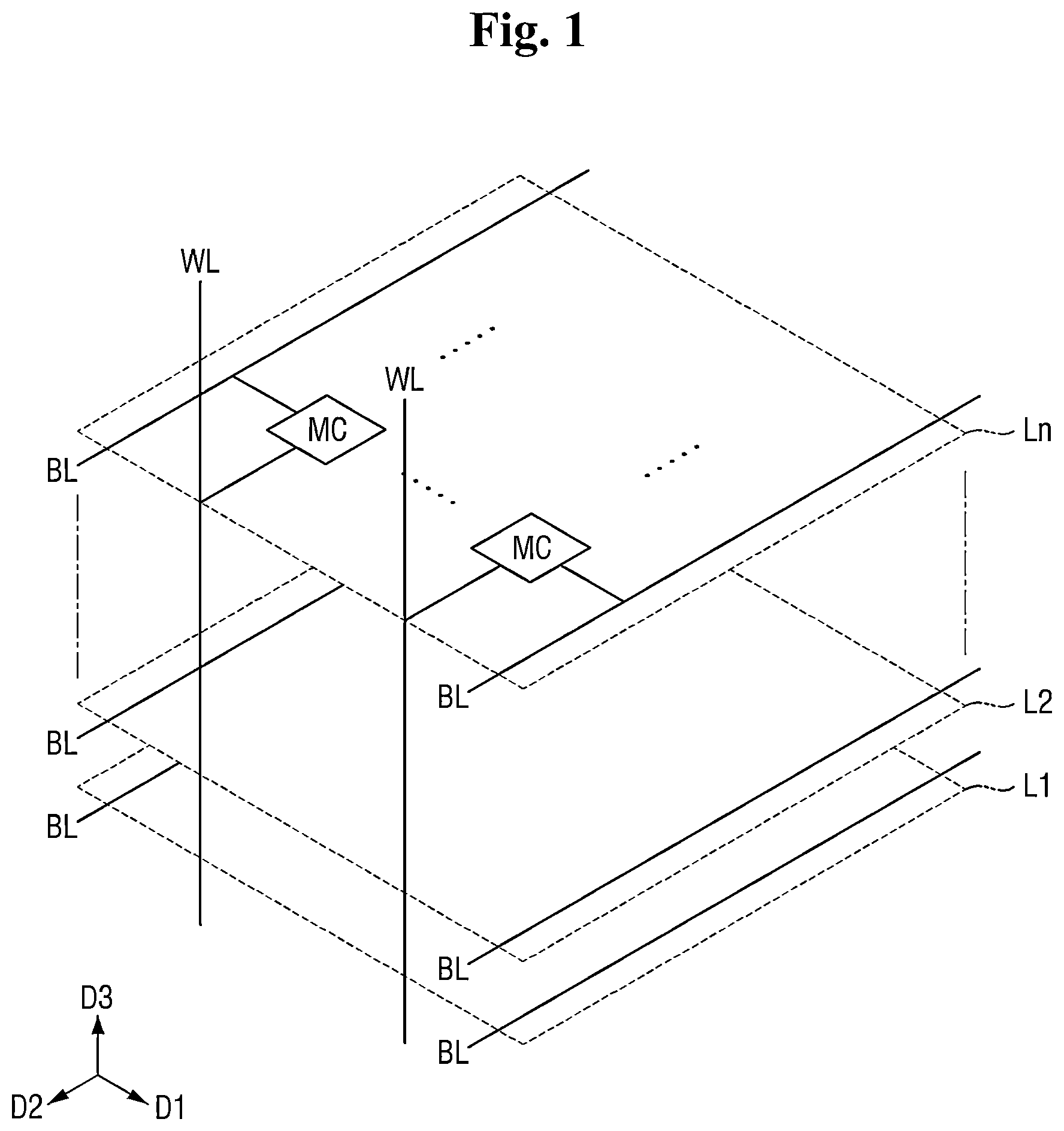
The above and other aspects and features of the present disclosure will become more apparent by describing in detail exemplary embodiments thereof with reference to the attached drawings, in which: is a schematic view of a semiconductor device according to some embodiments of the present disclosure; is a circuit diagram of an n-th layer of ; illustrates regions included in the n-th layer Ln of ; is a perspective view of a semiconductor device according to some embodiments of the present disclosure; is an enlarged perspective view illustrating first and second layers of ; is an enlarged perspective view of an area Q 1 of ; illustrates a wordline of ; is a cross-sectional view taken along line A-A of or 7 ; illustrates a top electrode of ; is a layout view of a semiconductor device according to some embodiments of the present disclosure; is an enlarged layout view of an area Q 2 of ; illustrates the relationship between an isolation insulating film and wordlines; is a cross-sectional view taken along line C-C of ; is a cross-sectional view taken along line D-D of ; is a layout view illustrating how bitlines and bitline contacts are connected in a semiconductor device according to some embodiments of the present disclosure; is a cross-sectional view taken along line E-E of ; is a flowchart illustrating a method of fabricating a semiconductor device according to some embodiments of the present disclosure; through 27 are cross-sectional views illustrating intermediate steps of the method of ; and through 32 are cross-sectional views illustrating how to form bitlines of a semiconductor device according to some embodiments of the present disclosure.
DETAILED DESCRIPTION
Preferred embodiments of the present disclosure will be described in detail with reference to the accompanying drawings. The present disclosure and methods of accomplishing the same may be understood more readily by reference to the following detailed description of embodiments and the accompanying drawings. However, the present disclosure may be embodied in many different forms, and should not be construed as being limited to the embodiments set forth herein. Rather, these embodiments are provided so that this disclosure will be through and complete and will fully convey the concept of the invention to those skilled in the art, and the present disclosure will only be defined by the appended claims. Like reference numbers designate like elements throughout the specification. Spatially relative terms, such as “beneath,” “below,” “lower,” “above,” “upper,” and the like, may be used herein for descriptive purposes, and, thereby, to describe one element or feature's relationship to another element(s) or feature(s) as illustrated in the drawings. Spatially relative terms are intended to encompass different orientations of an apparatus in use, operation, and/or manufacture in addition to the orientation depicted in the drawings. For example, if the apparatus in the drawings is turned over, elements described as “below” or “beneath” other elements or features would then be oriented “above” the other elements or features. Thus, the exemplary term “below” can encompass both an orientation of above and below. Furthermore, the apparatus may be otherwise oriented, and, as such, the spatially relative descriptors used herein interpreted accordingly. It will be understood that, although the terms “first”, “second”, etc. may be used herein to describe various elements, constituent elements and/or sections, the elements, constituent elements and/or sections should not be limited by these terms. These terms are only used to distinguish one element, constituent element, or section from another element, constituent element, or section. Thus, a first element, a first constituent element, or a first section discussed below should be termed a second element, a second constituent element, or a second section. Exemplary embodiments of the present disclosure will hereinafter be described with reference to the accompanying drawings. Like reference numerals indicate like elements through the specification, and thus, detailed descriptions thereof will be omitted. is a schematic view of a semiconductor device according to some embodiments of the present disclosure. is a circuit diagram of an n-th layer of . illustrates regions included in the n-th layer Ln of . Referring to , the semiconductor device includes a plurality of layers, i.e., first through n-th layers L 1 through Ln (where n is a natural number of 2 or greater), which are stacked. The first through n-th layers L 1 through Ln are stacked in a third direction D 3 . A plurality of memory cells MC are two-dimensionally arranged in each of the first through n-th layers L 1 through Ln. For example, the memory cells MC may be arranged in first and second directions D 1 and D 2 . The memory cells MC include cell transistors and capacitors. Bitlines BL may be installed in each of the first through n-th layers L 1 through Ln, and wordlines WL may be installed to penetrate the first through n-th layers L 1 through Ln. The bitlines BL may extend in the second direction D 2 , and the wordlines WL may extend in the third direction D 3 . The memory cells MC are electrically connected to the bitlines BL and the wordlines WL. The first direction D 1 may be parallel to the direction in which semiconductor patterns (or the bottom electrodes of capacitors) that will be described later extend, but the present disclosure is not limited thereto. The second direction D 2 may be parallel to the direction in which the bitlines BL extend, but the present disclosure is not limited thereto. The third direction D 3 may be parallel to a direction in which the wordlines WL extend, but the present disclosure is not limited thereto. The structure of the n-th layer Ln will hereinafter be described with reference to . Referring to , bitlines BL 1 and BL 2 extend in the second direction D 2 and are disposed to be spaced apart from each other. Wordlines WL 11 , WL 12 , WL 21 , and WL 22 are disposed to extend in the third direction D 3 . A first memory cell MC 1 is connected between the bitline BL 1 and the wordline WL 11 . The source of the first memory cell MC 1 is connected to the bitline BL 1 , the gate of the first memory cell MC 1 is connected to the wordline WL 11 , and the drain of the first memory cell MC 1 is connected to a capacitor C 1 . A second memory cell MC 2 is connected between the bitline BL 2 and the wordline WL 21 . The source of the second memory cell MC 2 is connected to the bitline BL 2 , the gate of the second memory cell MC 2 is connected to the wordline WL 21 , and the drain of the second memory cell MC 2 is connected to a capacitor C 2 . A third memory cell MC 3 is connected between the bitline BL 1 and the wordline WL 12 . The source of the third memory cell MC 3 is connected to the bitline BL 1 , the gate of the third memory cell MC 3 is connected to the wordline WL 12 , and the drain of the third memory cell MC 3 is connected to a capacitor C 3 . A fourth memory cell MC 4 is connected between the bitline BL 2 and the wordline WL 22 . The source of the fourth memory cell MC 4 is connected to the bitline BL 2 , the gate of the fourth memory cell MC 4 is connected to the wordline WL 22 , and the drain of the fourth memory cell MC 4 is connected to a capacitor C 4 . Referring to , the n-th layer Ln (or a substrate where the n-th layer Ln is formed) may include a capacitor region CR and first and second switching regions SW 1 and SW 2 , which are disposed on both sides of the capacitor region CR. A plurality of capacitors, i.e., first through fourth capacitors C 1 through C 4 , are disposed in the capacitor region CR. Cell transistors, i.e., first through fourth transistors TR 1 through TR 4 , are disposed in the first or second switching region SW 1 or SW 2 . The first through fourth cell transistors TR 1 through TR 4 may be disposed in a staggered (or zigzag) fashion. For example, the first cell transistor TR 1 , which corresponds to the first capacitor C 1 , may be disposed in the first switching region SW 1 , the second cell transistor TR 2 , which corresponds to the second capacitor C 2 adjacent to the first capacitor C 1 , may be disposed in the second switching region SW 2 , the third cell transistor TR 3 , which corresponds to the third capacitor C 3 adjacent to the second capacitor C 2 , may be disposed in the first switching region SW 1 , and the fourth cell transistor TR 4 , which corresponds to the fourth capacitor C 4 adjacent to the third capacitor C 3 , may be disposed in the second switching region SW 2 . is a perspective view of a semiconductor device according to some embodiments of the present disclosure. is an enlarged perspective view illustrating the first and second layers L 1 and L 2 of . is an enlarged perspective view of an area Q 1 of . For convenience, the top electrodes of capacitors are not illustrated in through 6 . Referring to , the semiconductor device includes a plurality of first through n-th layers L 1 through Ln, which are stacked in a third direction D 3 , and interlayer insulating films DI 1 through DIn are disposed between the first through n-th layers L 1 through Ln. Referring to , the first layer L 1 includes a plurality of semiconductor patterns S 11 , S 12 , S 13 , and S 14 , which are spaced apart from one another and extend in a first direction D 1 . The layer L 1 also includes bitlines BL 11 and BL 12 , which are spaced apart from each other and extend in a second direction D 2 . The second layer L 2 includes a plurality of semiconductor patterns S 21 , S 22 , S 23 , and S 24 , which are spaced apart from one another and extend in the first direction D 1 . The second layer L 2 also includes bitlines BL 21 and BL 22 , which are spaced apart from each other and extend in the second direction D 2 . The layer Ln includes a plurality of semiconductor patterns Sn 1 , Sn 2 , Sn 3 , and Sn 4 , which are spaced apart from one another and extend in the first direction D 1 . The layer Ln also includes bitlines BLn 1 and BLn 2 , which are spaced apart from each other and extend in the second direction D 2 . Referring to , the semiconductor pattern S 22 , for example, may be divided into a source S, a channel C, a drain D, and a bottom electrode BE 22 . The semiconductor pattern S 22 may include, for example, silicon (Si), but the present disclosure is not limited thereto. The source S, the drain D, and the bottom electrode BE 22 may be, for example, impurity regions doped with n-type impurities. A capacitor insulating film CD 22 is formed to surround the bottom electrode BE 22 . The capacitor insulating film CD 22 may be formed to surround the four sides of the bottom electrode BE 22 . The capacitor insulating film CD 22 may include, for example, a high-k material, but the present disclosure is not limited thereto. A gate insulating film GD 22 is formed to surround the channel C. The gate insulating film GD 22 may be formed to surround the four sides of the channel C. The gate insulating film GD 22 may include, for example, at least one of an oxide film, a nitride film, and a high-k material, but the present disclosure is not limited thereto. Referring again to , channels C of the first through n-th layers L 1 through Ln, which are stacked in the third direction D 3 , may be electrically connected by the wordlines WL 11 , WL 12 , WL 21 , and WL 22 , but the present disclosure is not limited thereto. Specifically, the wordline WL 11 electrically connects the channels C of the semiconductor patterns S 12 , S 22 , . . . , and Sn 2 in a vertical direction, the wordline WL 12 electrically connects the channels C of the semiconductor patterns S 14 , S 24 , . . . , Sn 4 in the vertical direction, the wordline WL 21 electrically connects the channels C of the semiconductor patterns S 11 , S 21 , . . . , Sn 1 in the vertical direction, and the wordline WL 22 electrically connects the channels C of the semiconductor patterns S 13 , S 23 , . . . , Sn 3 in the vertical direction. Isolation insulating films SAD 11 , SAD 12 , SAD 21 , and SAD 22 are formed to penetrate the first through n-th layers L 1 through Ln, which are stacked in the third direction D 3 . The isolation insulating films SAD 11 , SAD 12 , SAD 21 , and SAD 22 are disposed between the wordlines WL 11 , WL 12 , WL 21 , and WL 22 to insulate the wordlines WL 11 , WL 12 , WL 21 , and WL 22 from one another. Specifically, the isolation insulating film SAD 12 is disposed between the wordlines WL 11 and WL 12 in the second direction D 2 , and the isolation insulating film SAD 21 is disposed between the wordlines WL 21 and WL 22 in the second direction D 2 . A source S, a channel C, and a drain D (of a cell transistor) may be positioned on one side, in the first direction D 1 , of the bottom electrode BEn 2 of the semiconductor pattern Sn 2 , and the isolation insulating film SAD 21 may be positioned on the other side, in the first direction D 1 , of the bottom electrode BEn 2 . Accordingly, one side of the semiconductor pattern Sn 2 may be electrically connected to, for example, the bitline BLn 1 , and the other side of the semiconductor pattern SN 2 may be insulated from, for example, the bitline BLn 2 , by the isolation insulating film SAD 21 . As illustrated in , the wordlines WL 11 , WL 12 , WL 21 , and WL 22 may be disposed in a staggered (or zigzag) fashion. The wordlines WL 11 , WL 12 , WL 21 , and WL 22 are not installed in one switching region (e.g., the first switching region SW 1 of ). The wordlines WL 11 and WL 12 are disposed in the first switching region SW 1 , and the wordlines WL 21 and WL 22 are disposed in the second switching region SW 2 . The wordlines WL 11 and WL 12 , which are connected to the semiconductor patterns Sn 2 and Sn 4 , respectively, are disposed in the first switching region SW 1 , and the wordlines WL 21 and WL 22 , which are connected to the semiconductor patterns Sn 1 and Sn 3 , respectively, are disposed in the second switching region SW 2 . The isolation insulating film SAD 11 , the wordline WL 11 , the isolation insulating film SAD 12 , and the wordline WL 12 are sequentially disposed in the second direction D 2 in the first switching region SW 1 . The wordline WL 21 , the isolation insulating film SAD 21 , the wordline WL 22 , and the isolation insulating film SAD 22 are sequentially disposed in the second direction D 2 in the second switching region SW 2 . Referring to , CDn 1 through CDn 4 refer to capacitor insulating films formed in the semiconductor patterns Sn 1 , Sn 2 , Sn 3 , and Sn 4 in the n-ty layer Ln. illustrates the wordline WL 11 of . is a cross-sectional view taken along line A-A of or 7 . illustrates a top electrode TE 11 of . Referring to , the semiconductor patterns S 12 , S 22 , . . . , and Sn 2 are stacked in the third direction D 3 . Gate insulating films GD 12 , GD 22 , . . . , and GDn 2 are formed to surround parts of the semiconductor patterns S 12 , S 22 , . . . , and Sn 2 (i.e., the channels C of the semiconductor patterns S 12 , S 22 , . . . , and Sn 2 ). The gate insulating films GD 12 , GD 22 , . . . , and GDn 2 are formed to surround the four sides of their respective channels C. The wordline WL 11 extends in the third direction D 3 and is formed to surround the semiconductor patterns S 12 , S 22 , . . . , and Sn 2 . Referring to , the semiconductor patterns S 12 , S 22 , . . . , and Sn 2 are stacked in the third direction D 3 . Capacitor insulating films CD 12 , CD 22 , . . . , and CDn 2 are formed to surround the semiconductor patterns S 12 , S 22 , . . . , and Sn 2 (i.e., the bottom electrodes BE 12 , BE 22 , . . . , and BEn 2 ), respectively. The capacitor insulating films CD 12 , CD 22 , . . . , and CDn 2 are formed to surround the four sides of their respective bottom electrodes BE 12 , BE 22 , . . . , and BEn 2 . The top electrode TE 11 extends in the third direction D 3 and is formed to surround the semiconductor patterns S 12 , S 22 , . . . , and Sn 2 (i.e., the bottom electrodes BE 12 , BE 22 , . . . , and BEn 2 ). is a layout view of a semiconductor device according to some embodiments of the present disclosure. is an enlarged layout view of an area Q 2 of . illustrates the relationship between an isolation insulating film and wordlines. is a cross-sectional view taken along line C-C of . is a cross-sectional view taken along line D-D of . Referring to , the semiconductor device includes a plurality of banks, i.e., first and second banks BA and BB. The first and second banks BA and BB are illustrated as being disposed in parallel in a first direction D 1 , but the present disclosure is not limited thereto. The first bank BA includes a capacitor region CR 1 and first and second switching regions SW 11 and SW 12 , which are disposed on both sides of the capacitor region CR 1 . Similarly, the second bank BB includes a capacitor region CR 2 and first and second switching regions SW 21 and SW 22 , which are disposed on both sides of the capacitor region CR 2 . Referring to , a plurality of semiconductor patterns S 1 through S 7 are disposed in the first bank BA to extend in the first direction D 1 . The semiconductor patterns S 1 through S 7 are spaced apart from one another in a second direction D 2 . Wordlines WL 1 , WL 2 , WL 3 , and WL 4 , which are electrically connected to the channels of the semiconductor patterns S 1 , S 3 , S 5 , and S 7 , respectively, and extend in a third direction D 3 , are disposed in the first switching region SW 11 . Isolation insulating films SAD 1 , SAD 2 , and SAD 3 , which extend in the third direction D 3 , are disposed to penetrate the semiconductor patterns S 2 , S 4 , and S 6 , respectively. The wordlines WL 1 through WL 4 may be disposed in a staggered (or zigzag) fashion in the first switching region SW 11 . In other words, a first distance DST 1 , in the first direction D 1 , between a bitline BL 1 and the wordline WL 1 or WL 3 may differ from a second distance DST 2 , in the first direction D 1 , between the bitline BL 1 and the wordline WL 2 or WL 4 . An imaginary line connecting the centers of the wordlines WL 1 and WL 3 does not overlap with the wordline WL 2 because the wordline WL 2 is disposed closer than the wordlines WL 1 and WL 3 to the capacitor region CR 1 . The isolation insulating films SAD 1 through SAD 3 are disposed between the wordlines WL 1 through WL 4 . For example, the isolation insulating film SAD 1 prevents a pair of adjacent wordlines in the second direction D 2 , i.e., the wordlines WL 1 and WL 2 , from being short-circuited. The isolation insulating film SAD 1 may be self-aligned while being in contact with the wordlines WL 1 and WL 2 . As will be described later, the isolation insulating film SAD 1 is formed by forming a trench to have a low etch rate for the material of the wordlines WL 1 and WL 2 (i.e., a metal) and filling the trench with an insulating film. As the isolation insulating film SAD 1 is self-aligned, the isolation insulating film SAD 1 can properly insulate the wordlines WL 1 and WL 2 , which are adjacent to each other, even in a narrow region. Referring to , a width W 3 , in the first direction D 1 , of the isolation insulating film SAD 1 is greater than a width W 1 , in the first direction D 1 , of the wordline WL 1 or a width W 2 , in the first direction D 1 , of the wordline WL 2 . As the wordlines WL 1 and WL 2 are disposed in a staggered manner, the isolation insulating film SAD 1 is formed to extend long in the first direction D 1 to properly insulate the wordlines WL 1 and WL 2 . Referring again to , isolation insulating films SAD 4 , SAD 5 , SAD 6 , and SAD 7 , which extend in the third direction D 3 , are disposed in the second switching region SW 12 to penetrate the semiconductor patterns S 1 , S 3 , S 5 , and S 7 , respectively. Also, wordlines WL 5 , WL 6 , and WL 7 , which are electrically connected to the channels C of the semiconductor patterns S 2 , S 4 , and S 6 and extend in the third direction D 3 , are disposed in the second switching region SW 12 . The wordlines WL 5 , WL 6 , and WL 7 may be disposed in a staggered (or zigzag) fashion in the second switching region SW 12 . In other words, the distance, in the first direction D 1 , between a bitline BL 2 and the wordline WL 5 or WL 7 may differ from the distance, in the first direction D 1 , between the bitline BL 2 and the wordline WL 6 . An imaginary line connecting the centers of the wordlines WL 5 and WL 7 does not overlap with the wordline WL 6 because the wordline WL 6 is disposed closer than the wordlines WL 5 and WL 7 to the capacitor region CR 1 . A capacitor insulating film is formed in the capacitor region CR 1 to surround the semiconductor patterns S 1 through S 7 , and the top electrode TE is formed on the capacitor insulating film. Referring to , a plurality of semiconductor patterns S 1 may be disposed to extend in the first direction D 1 across the first switching region SW 11 , the capacitor region CR 1 , and the second switching region SW 12 . The semiconductor patterns S 1 are stacked in the third direction D 3 . Bitlines BL 1 , which are connected to first sides of the semiconductor patterns S 1 , is disposed in the first switching region SW 11 . Bitlines BL 2 , which are connected to second sides of the semiconductor patterns S 1 , is disposed in the second switching region SW 12 . The semiconductor patterns S 1 are electrically isolated from one another by the isolation insulating film SAD 4 . Thus, the semiconductor patterns S 1 may receive voltages and/or signals from the bitlines BL 1 , but not from the bitlines BL 2 . The semiconductor patterns S 1 may be used as sources S, channels C, and drains D of cell transistors and as bottom electrodes BE of capacitors. Gate insulating films GD are formed to surround the channels C, and capacitor insulating films CD are formed to surround the bottom electrodes BE. A top electrode TE, which surrounds the bottom electrodes BE and the capacitor insulating films CD and extends in the third direction D 3 , is formed. Referring to , semiconductor patterns S 1 are disposed on a substrate to be stacked in the third direction D 3 , semiconductor patterns S 3 are disposed on the substrate to be stacked in the third direction D 3 , and semiconductor patterns S 5 are disposed on the substrate to be stacked in the third direction D 3 . The semiconductor patterns S 1 , the semiconductor patterns S 3 , and the semiconductor patterns S 5 are spaced apart from one another in the second direction D 2 . The semiconductor patterns S 1 , which are stacked, are electrically connected by the wordline WL 1 , and the semiconductor patterns S 5 , which are stacked, are electrically connected by the wordline WL 3 . The semiconductor patterns S 3 , which are stacked, are surrounded by an insulating film. The isolation insulating film SAD 1 is disposed between the semiconductor patterns S 1 and the semiconductor patterns S 3 , which are adjacent to the semiconductor patterns S 1 . The isolation insulating film SAD 2 is disposed between the semiconductor patterns S 3 and the semiconductor patterns S 5 , which are adjacent to the semiconductor patterns S 3 . is a layout view illustrating how bitlines and bitline contacts are connected in a semiconductor device according to some embodiments of the present disclosure. is a cross-sectional view taken along line E-E of . Referring to , the semiconductor device includes a plurality of layers L 1 through L 6 , which are stacked. Sides of the layers L 1 through L 6 may form a stepwise structure. That is, each of the layers L 1 through L 6 may be smaller in size than its overlying layer. For example, the second layer L 2 may be smaller in size than the first layer L 1 . Thus, the first layer L 1 may include an exposed region EXP 1 , which is exposed by the second layer L 2 . A bitline BL 11 of the first layer L 1 is also exposed by the second layer L 2 . Similarly, the layers L 2 , L 3 , L 4 , L 5 , and L 6 may include exposed regions EXP 2 , EXP 3 , EXP 4 , EXP 5 , and EXP 6 , respectively. Bitlines BL 12 , BL 13 , BL 14 , and BL 14 of the layers L 2 , L 3 , L 4 , and L 5 are exposed by the layers L 3 , L 4 , L 5 , and L 6 , respectively. Bitline contacts BLC 1 , BLC 2 , BLC 3 , BLC 4 , BLC 5 , and BLC 6 , which are for providing signals to the bitlines BL 11 , BL 12 , BL 13 , BL 14 , and BL 15 and a bitline BL 16 , respectively, are formed in the exposed regions EXP 1 , EXP 2 , EXP 3 , EXP 4 , EXP 5 , and EXP 6 , respectively. is a flowchart illustrating a method of fabricating a semiconductor device according to some embodiments of the present disclosure. through 27 are cross-sectional views illustrating intermediate steps of the method of . is a flowchart illustrating how to form the wordlines WL 1 and WL 2 and the isolation insulating films SAD 1 and SAD 2 of in a first switching region SW 11 . Referring to , a stack structure is formed by alternately depositing first semiconductor (e.g., Si) layers 101 and second semiconductor (e.g., SiGe) layers 102 on a substrate (S 110 ). Thereafter, referring to , wordlines, which penetrate the stack structure, are formed (S 120 ). Specifically, referring to , a plurality of trenches 110 are formed in a switching region (e.g., the first switching region SW 11 of ) by patterning the stack structure. Thereafter, referring to , an insulating film 120 is formed to fill the trenches 110 . The insulating film 120 may include at least one of an oxide film, a nitride film, and an oxynitride film. For example, the insulating film 120 may be an oxide film including a spin-on-dielectric (SOD) material with excellent gap-fill characteristics. The insulating film 120 may be formed by applying an insulating material onto the substrate through spinning and performing planarization (e.g., chemical mechanical planarization (CMP)). Thereafter, referring to , wordline forming regions 130 a and 130 b are formed. A stack of semiconductor patterns S 1 is positioned in the wordline forming region 130 a , and a stack of semiconductor patterns S 5 is positioned in the wordline forming region 130 b . The insulating film 120 is removed first from the wordline forming regions 130 a and 130 b , and the second semiconductor layers 102 are removed from the wordline forming regions 130 a and 130 b . The first semiconductor layers 101 are exposed in the wordline forming regions 130 a and 130 b . A gate insulating film is formed to surround the exposed first semiconductor layers 101 . The first semiconductor layers 101 in the wordline forming region 130 a correspond to the semiconductor patterns S 1 of . The first semiconductor layers 101 in the wordline forming region 130 b correspond to the semiconductor patterns S 5 of . Thereafter, referring to , wordlines WL 1 and WL 2 are formed by filling the wordline forming regions 130 a and 130 b with a metal. Referring again to , isolation insulating films, which penetrate the stack structure and are self-aligned, are formed (S 130 ). Specifically, referring to , the insulating film 120 is removed, leaving the wordlines WL 1 and WL 2 in the first switching region SW 11 . Thereafter, referring to , the second semiconductor layers 102 are removed. The first semiconductor layers 101 remain between the wordlines WL 1 and WL 2 . The remaining first semiconductor layers 101 correspond to the semiconductor patterns S 2 , S 3 , and S 4 of . Thereafter, referring to , an insulating film 121 is formed on the structure illustrated in . The insulating film 121 is formed to sufficiently cover semiconductor patterns S 2 , semiconductor patterns S 3 , and semiconductor patterns S 4 . Thereafter, referring to , a mask pattern is formed on the structure illustrated in , and trenches 131 a and 131 b are formed using the mask pattern. The trenches 131 a and 131 b are for forming isolation insulating films SAD 1 and SAD 2 . Some of the semiconductor patterns S 2 and some of the semiconductor patterns S 4 are removed from the first switching region SW 11 due to the trenches 131 a and 131 b. The trenches 131 a and 131 b may be formed using a method that does not remove the wordlines WL 1 and WL 2 or can minimize damage to the wordlines WL 1 and WL 2 . As a result, the trenches 131 a and 131 b may be formed to be in contact with the wordlines WL 1 and WL 2 . Thereafter, referring to , the isolation insulating films SAD 1 and SAD 2 are formed by filling the trenches 131 a and 131 b with an insulating film. For example, an insulating film may be formed by atomic layer deposition (ALD) to fill the trenches 131 a and 131 b . The isolation insulating films SAD 1 and SAD 2 may be in contact with the wordlines WL 1 and WL 2 and may be self-aligned. Thereafter, a planarization process may optionally be performed to remove parts of the insulating film 121 and the isolation insulating films SAD 1 and SAD 2 . As a result, the structure illustrated in may be obtained. through 32 are cross-sectional views illustrating how to form bitlines of a semiconductor device according to some embodiments of the present disclosure. Referring to , a hard mask 209 is formed on a structure in which a plurality of semiconductor patterns S 1 are stacked and wordlines WL are formed. Interlayer insulating films DI are formed between the semiconductor patterns S 1 . The interlayer insulating films DI may be oxide films. Referring to , a trench 210 is formed in the structure of , using the hard mask 209 . Referring to , bitline forming regions 220 are formed by removing parts of the interlayer insulating films (or oxide films) exposed by the trench 210 via horizontal etching. Referring to , the trench 210 and the bitline forming regions 220 are filled with a metal film 230 . For example, the metal film 230 may be formed by ALD. Referring to , the entire metal film 230 except for parts that fill the bitline forming regions 220 is removed. The parts of the metal film 230 that remain in the bitline forming regions 220 correspond to bitlines BL. Although embodiments of the present invention have been described with reference to the above and the accompanying drawings, it will be appreciated by those of ordinary skill in the art that the present invention can be embodied in other specific forms without departing from its essential character. The embodiments described above should therefore be considered in all respects to be illustrative and not restrictive.
Figures (20)
Citations
This patent cites (14)
- US7355230
- US10784272
- US11100958
- US11355509
- US11844212
- US2011/0221010
- US2019/0019722
- US2019/0206869
- US2020/0066856
- US2020/0111793
- US2021/0265357
- US2022/0367514
- US10-2019-0060251
- US10-2020-0039075