Integrated Circuit Device Including N-channel Metal-oxide Semiconductor (NMOS) Transistor Region and a P-channel Metal-oxide Semiconductor (PMOS) Transistor Region
Abstract
An integrated circuit device including a substrate including first and second device regions; a first fin active region on the first device region; a second fin active region on the second device region; an isolation film covering side walls of the active regions; gate cut insulating patterns on the isolation film on the device regions; a gate line extending on the fin active regions, the gate line having a length limited by the gate cut insulating patterns; and an inter-region insulating pattern on the isolation film between the fin active regions and at least partially penetrating the gate line in a vertical direction, wherein the inter-region insulating pattern has a bottom surface proximate to the substrate, a top surface distal to the substrate, and a side wall linearly extending from the bottom to the top surface.
Claims (20)
1. An integrated circuit device, comprising: a substrate including a first device region and a second device region; at least one first channel region extending in a first horizontal direction on the first device region; at least one second channel region extending in the first horizontal direction on the second device region; an isolation film covering opposite side walls of each of the at least one first channel region and the at least one second channel region; a first gate cut insulating pattern on the isolation film on the first device region; a second gate cut insulating pattern on the isolation film on the second device region; a gate line extending on the first device region and the second device region in a second horizontal direction that crosses the first horizontal direction, the gate line having a length in the second horizontal direction limited by the first gate cut insulating pattern and the second gate cut insulating pattern, each of the at least one first channel region and the at least one second channel region being surrounded by the gate line; and an inter-region insulating pattern on the isolation film between the at least one first channel region and the at least one second channel region, the inter-region insulating pattern partially penetrating the gate line in a vertical direction, wherein the inter-region insulating pattern has a sidewall linearly extended in the vertical direction without a stepped portion.
12. An integrated circuit device, comprising: a substrate including a first device region and a second device region separated from the first device region; at least one first fin active region extending in a first horizontal direction on the first device region; at least one second fin active region extending in the first horizontal direction on the second device region; an isolation film covering opposite side walls of each of the at least one first fin active region and the at least one second fin active region; a gate line extending on the first device region and the second device region in a second horizontal direction that crosses the first horizontal direction; at least one first channel region on the at least one first fin active region, the at least one first channel region surrounded by the gate line; at least one second channel region on the at least one second fin active region, the at least one second channel region surrounded by the gate line; and an inter-region insulating pattern on the isolation film between the at least one first channel region and the at least one second channel region, the inter-region insulating pattern partially penetrating the gate line in a vertical direction, wherein the inter-region insulating pattern has a sidewall linearly extended in the vertical direction without a stepped portion.
20. An integrated circuit device, comprising: a substrate including an N-channel metal-oxide semiconductor (NMOS) transistor region and a P-channel MOS (PMOS) transistor region separated from the NMOS transistor region; at least one first channel region extending in a first horizontal direction on the NMOS transistor region; at least one second channel region extending in the first horizontal direction on the PMOS transistor region; an isolation film covering opposite side walls of each of the at least one first channel region and the at least one second channel region; a first gate cut insulating pattern on the isolation film on the NMOS transistor region and having a first height in a vertical direction; a second gate cut insulating pattern on the isolation film on the PMOS transistor region and having a second height in the vertical direction; a gate line extending on the NMOS transistor region and the PMOS transistor region in a second horizontal direction that crosses the first horizontal direction, the gate line having a length in the second horizontal direction limited by the first gate cut insulating pattern and the second gate cut insulating pattern, each of the at least one first channel region and the at least one second channel region being surrounded by the gate line; and an inter-region insulating pattern between the NMOS transistor region and the PMOS transistor region, the inter-region insulating pattern partially penetrating the gate line in the vertical direction and having a third height in the vertical direction that is less than each of the first height and the second height, wherein the inter-region insulating pattern has a sidewall linearly extending in the vertical direction without a stepped portion.
Show 17 dependent claims
2. The integrated circuit device as claimed in claim 1 , wherein the inter-region insulating pattern has a local surface planarly extended, the local surface facing the gate line.
3. The integrated circuit device as claimed in claim 1 , wherein the inter-region insulating pattern has a non-planar surface facing the gate line.
4. The integrated circuit device as claimed in claim 1 , wherein the isolation film has different shapes in the first device region and the second device region.
5. The integrated circuit device as claimed in claim 1 , wherein the inter-region insulating pattern has a bottom surface facing the substrate, the bottom surface being in contact with the isolation film.
6. The integrated circuit device as claimed in claim 1 , wherein the inter-region insulating pattern has a first sidewall and a second sidewall that are opposite to each other in the second horizontal direction, the first sidewall facing the at least one first channel region in the second horizontal direction, and the second sidewall facing the at least one second channel region in the second horizontal direction.
7. The integrated circuit device as claimed in claim 1 , wherein the at least one first channel region has a first topmost surface distal to the substrate, the at least one second channel region has a second topmost surface distal to the substrate, and the inter-region insulating pattern has a third topmost surface distal to the substrate, and wherein a level of each of the first topmost surface, the second topmost surface, and the third topmost surface is lower than a level of a topmost surface of the gate line.
8. The integrated circuit device as claimed in claim 1 , wherein the inter-region insulating pattern has a top surface distal to the substrate, the top surface being a non-planar surface.
9. The integrated circuit device as claimed in claim 1 , wherein: the gate line includes: a first portion covering the at least one first channel region on the first device region and having a first stack structure, a second portion covering the at least one second channel region on the second device region and having a second stack structure that is different from the first stack structure, and a gate connecting portion integrally connected to the first portion and the second portion and covering a top surface of the inter-region insulating pattern, and the gate connecting portion has a structure different from the first stack structure and the second stack structure.
10. The integrated circuit device as claimed in claim 1 , wherein: the gate line includes a first gate portion on the first device region and a second gate portion on the second device region, and the first gate portion is separated from the second gate portion with the inter-region insulating pattern between the first gate portion and the second gate portion in the second horizontal direction.
11. The integrated circuit device as claimed in claim 1 , wherein each of the first gate cut insulating pattern and the second gate cut insulating pattern has a bottom surface facing the substrate, the bottom surface being in contact with the isolation film.
13. The integrated circuit device as claimed in claim 12 , wherein the inter-region insulating pattern has a local surface planarly extended, the local surface facing the gate line.
14. The integrated circuit device as claimed in claim 12 , wherein the inter-region insulating pattern has a non-planar surface facing the gate line.
15. The integrated circuit device as claimed in claim 12 , wherein the isolation film has different shapes in the first device region and the second device region.
16. The integrated circuit device as claimed in claim 12 , wherein each of the at least one first fin active region and the at least one second fin active region has a width in the second horizontal direction, the width gradually decreasing as the distance from the substrate increases along the vertical direction.
17. The integrated circuit device as claimed in claim 12 , wherein the inter-region insulating pattern has a bottom surface facing the substrate, the bottom surface being in contact with the isolation film.
18. The integrated circuit device as claimed in claim 12 , wherein the at least one first channel region has a first topmost surface distal to the substrate, the at least one second channel region has a second topmost surface distal to the substrate, and the inter-region insulating pattern has a third topmost surface distal to the substrate, and wherein a level of each of the first topmost surface, the second topmost surface, and the third topmost surface is lower than a level of a topmost surface of the gate line.
19. The integrated circuit device as claimed in claim 12 , wherein the inter-region insulating pattern has a top surface distal to the substrate, the top surface being a non-planar surface.
Full Description
Show full text →
CROSS-REFERENCE TO RELATED APPLICATIONS
This is a continuation application that claims priority to U.S. patent application Ser. No. 18/212,304, filed on Jun. 21, 2023, which is a continuation of U.S. patent application Ser. No. 17/372,896, filed Jul. 12, 2021, which is now U.S. Pat. No. 11,710,739, issued on Jul. 7, 2023, the entire contents of which is are hereby incorporated by reference.
BACKGROUND
1. Field
Embodiments relate to an integrated circuit device.
2. Description of the Related Art
As the size of an integrated circuit device decreases, the integration density of field-effect transistors on a substrate may be increased. A horizontal nanosheet field-effect transistor (hNSFET) including a plurality of horizontal nanosheets stacked on one layout region has been considered.
SUMMARY
The embodiments may be realized by providing an integrated circuit device including a substrate including a first device region and a second device region; a first fin active region extending in a first horizontal direction on the first device region; a second fin active region extending in the first horizontal direction on the second device region; an isolation film covering opposite side walls of each of the first fin active region and the second fin active region; a plurality of gate cut insulating patterns on the isolation film on the first device region and the second device region; a gate line extending on the first fin active region and the second fin active region in a second horizontal direction that crosses the first horizontal direction, the gate line having a length in the second horizontal direction limited by the plurality of gate cut insulating patterns; and an inter-region insulating pattern on the isolation film between the first fin active region and the second fin active region and at least partially penetrating the gate line in a vertical direction, wherein the inter-region insulating pattern has a bottom surface proximate to the substrate, a top surface distal to the substrate, and a side wall linearly extending from the bottom surface to the top surface.
The embodiments may be realized by providing an integrated circuit device including a substrate including a first device region and a second device region separated from the first device region; a first fin active region extending in a first horizontal direction on the first device region; a second fin active region extending in the first horizontal direction on the second device region; an isolation film covering opposite side walls of each of the first fin active region and the second fin active region; a gate line extending on the first device region and the second device region in a second horizontal direction that crosses the first horizontal direction; a first nanosheet stack facing a first fin top of the first fin active region at a position separated from the first fin top in a vertical direction, the first nanosheet stack including at least one first nanosheet surrounded by the gate line; a second nanosheet stack facing a second fin top of the second fin active region at a position separated from the second fin top in the vertical direction, the second nanosheet stack including at least one second nanosheet surrounded by the gate line; and an inter-region insulating pattern on the isolation film between the first fin active region and the second fin active region and partially penetrating the gate line in the vertical direction, wherein the inter-region insulating pattern has a bottom surface contacting the isolation film, a top surface contacting the gate line, and a side wall linearly extending from the bottom surface to the top surface.
The embodiments may be realized by providing an integrated circuit device including a substrate including an N-channel metal-oxide semiconductor (NMOS) transistor region and a P-channel MOS (PMOS) transistor region separated from the NMOS transistor region; a first fin active region extending in a first horizontal direction on the NMOS transistor region; a second fin active region extending in the first horizontal direction on the PMOS transistor region; an isolation film covering opposite side walls of each of the first fin active region and the second fin active region; a plurality of gate cut insulating patterns on the isolation film on the NMOS transistor region and the PMOS transistor region and having a first height in a vertical direction; a gate line extending on the NMOS transistor region and the PMOS transistor region in a second horizontal direction that crosses the first horizontal direction; a first nanosheet stack on the first fin active region and including at least one first nanosheet surrounded by the gate line; a second nanosheet stack on the second fin active region and including at least one second nanosheet surrounded by the gate line; and an inter-region insulating pattern between the NMOS transistor region and the PMOS transistor region, partially penetrating the gate line in the vertical direction, and having a second height in the vertical direction that is less than the first height, wherein the inter-region insulating pattern has a bottom surface contacting the isolation film, a top surface contacting the gate line, and a side wall linearly extending from the bottom surface to the top surface.
BRIEF DESCRIPTION OF THE DRAWINGS
Features will be apparent to those of skill in the art by describing in detail exemplary embodiments with reference to the attached drawings in which:
is a plane layout diagram of partial configurations of an integrated circuit device, according to embodiments;
A is a cross-sectional view of a partial configuration of a cross-section taken along line X 1 -X 1 ′ in ; B is a cross-sectional view of a partial configuration of a cross-section taken along line X 2 -X 2 ′ in ; C is a cross-sectional view of a partial configuration of a cross-section taken along line Y 1 -Y 1 ′ in ;
is a cross-sectional view of an integrated circuit device according to some embodiments;
is a cross-sectional view of an integrated circuit device according to some embodiments;
is a cross-sectional view of an integrated circuit device according to some embodiments;
is a cross-sectional view of an integrated circuit device according to some embodiments;
is a cross-sectional view of an integrated circuit device according to some embodiments;
is a plane layout diagram of partial configurations of an integrated circuit device, according to embodiments;
is a cross-sectional view of a partial configuration of a cross-section taken along line Y 1 -Y 1 ′ in ;
is a cross-sectional view of an integrated circuit device according to some embodiments;
A, 11 B, 11 C, 12 A, 12 B, 12 C, 13 A, 13 B, 13 C, 14 A, 14 B, 14 C, 15 A, 15 B, 15 C, 16 A, 16 B, 16 C, 17 A, 17 B, 17 C , 18 , 19 , 20 , 21 , 22 , 23 , 24 , and 25 are cross-sectional views of stages in a method of manufacturing an integrated circuit device, according to embodiments, in which A, 12 A , . . . , and 17 A show a partial configuration of a portion corresponding to the cross-section taken along the line X 1 -X 1 ′ in , B, 12 B , . . . , and 17 B show a partial configuration of a portion corresponding to the cross-section taken along the line X 2 -X 2 ′ in , and C, 12 C , . . . , and 17 C and through 25 show a partial configuration of a portion corresponding to the cross-section taken along the line Y 1 -Y 1 ′ in ;
is a cross-sectional view of a stage in a method of manufacturing an integrated circuit device, according to some embodiments; and
A, 27 B, 27 C, 27 D, 27 E, and 27 F are cross-sectional views of stages in a method of manufacturing an integrated circuit device, according to some embodiments.
DETAILED DESCRIPTION
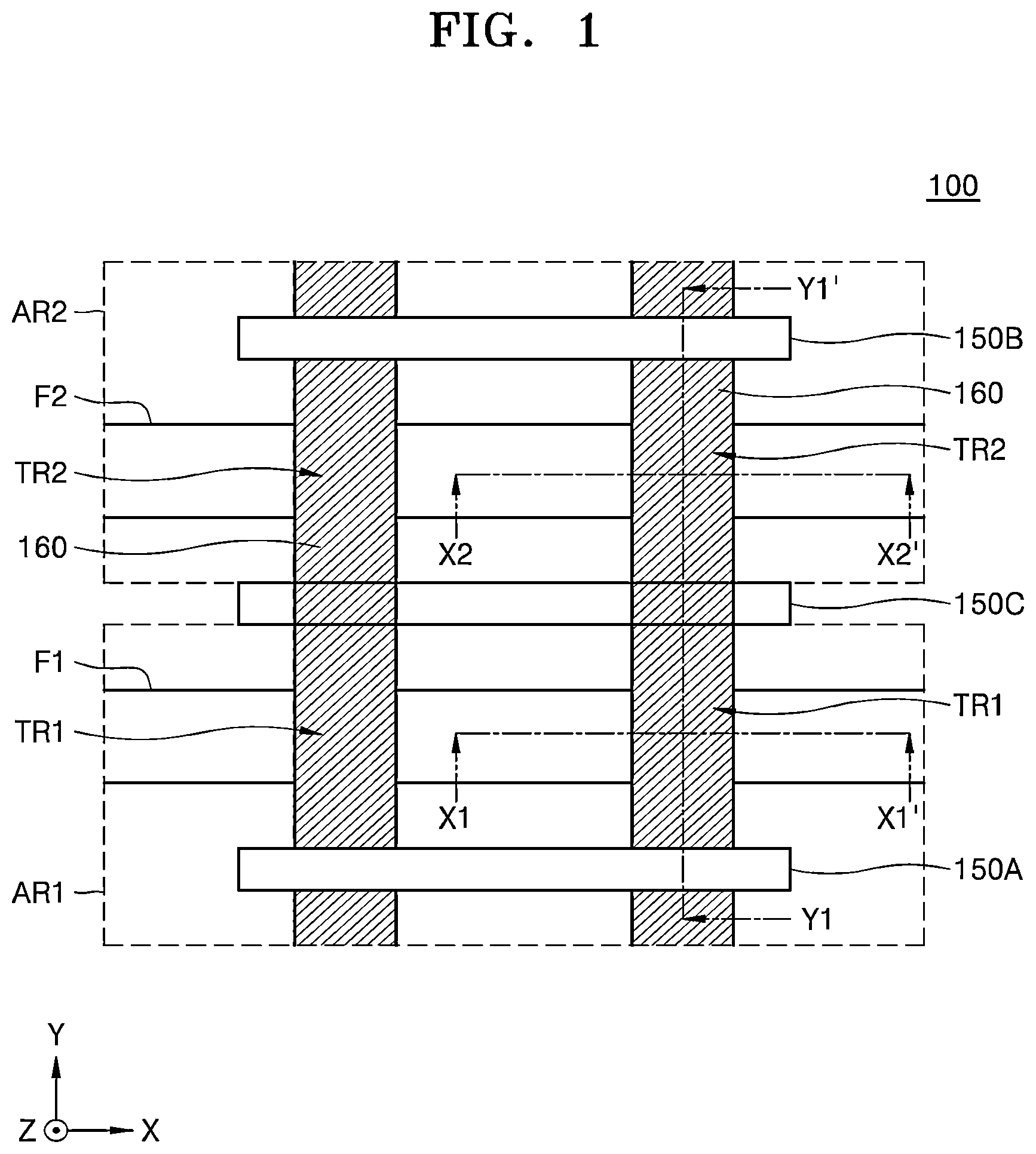
is a plane layout diagram of partial configurations of an integrated circuit device 100 , according to embodiments. A is a cross-sectional view of a partial configuration of a cross-section taken along line X 1 -X 1 ′ in ; B is a cross-sectional view showing a partial configuration of a cross-section taken along line X 2 -X 2 ′ in ; and C is a cross-sectional view of a partial configuration of a cross-section taken along line Y 1 -Y 1 ′ in .
Referring to and A through 2 C , the integrated circuit device 100 may include a substrate 102 , which includes a first device region AR 1 and a second device region AR 2 , and a plurality of fin active regions F 1 and F 2 , which respectively protrude from the first and second device regions AR 1 and AR 2 of the substrate 102 in a vertical direction (a Z direction). The fin active regions F 1 and F 2 may extend to be parallel with each other in a first horizontal direction (an X direction). The fin active regions F 1 and F 2 may include a first fin active region F 1 , which protrudes from the first device region AR 1 of the substrate 102 in the vertical direction, and a second fin active region F 2 , which protrudes from the second device region AR 2 of the substrate 102 in the vertical direction. In an implementation, as illustrated in , one first fin active region F 1 may be on the first device region AR 1 and one second fin active region F 2 may be on the second device region AR 2 , or a plurality of fin active regions may be arranged on each of the first and second device regions AR 1 and AR 2 .
The substrate 102 may include a semiconductor such as Si or Ge or a compound semiconductor such as SiGe, SiC, GaAs, InAs, InGaAs, or InP. Each of the terms “SiGe”, “SiC”, “GaAs”, “InAs”, “InGaAs”, and “InP” used herein indicates a material composed of elements included in each term and is not a chemical equation representing stoichiometric relationships. The substrate 102 may include a conductive region, e.g., an impurity-doped well or an impurity-doped structure. As used herein, the term “or” is not an exclusive term, e.g., “A or B” would include A, B, or A and B.
An isolation film 112 , which covers both, e.g., opposite) side walls of each of the first and second fin active regions F 1 and F 2 , may be in the substrate 102 . The isolation film 112 may include an oxide film, a nitride film, or a combination thereof. The first fin active region F 1 may protrude upwardly through the isolation film 112 in a fin shape on the first device region AR 1 , and the second fin active region F 2 may protrude upwardly through the isolation film 112 in a fin shape on the second device region AR 2 .
A plurality of gate lines 160 may extend lengthwise on the first and second fin active regions F 1 and F 2 in a second horizontal direction (a Y direction) that crosses the first horizontal direction. Each of a plurality of nanosheet stacks NSS may be above or on a fin top FT of one of the first and second fin active regions F 1 and F 2 at an intersection between a corresponding one of the first and second fin active regions F 1 and F 2 and one of the gate lines 160 . Each of the nanosheet stacks NSS may face the fin top FT of a corresponding one of the first and second fin active regions F 1 and F 2 at a position separated in the vertical direction from the corresponding one of the first and second fin active regions F 1 and F 2 . The term “nanosheet” used herein refers to a conductive structure having a cross-section that is substantially perpendicular to a direction in which electric current flows. It will be understood that the nanosheet may include a nanowire.
Each of the nanosheet stacks NSS may include a plurality of nanosheets, which overlap each other above the fin top FT of a corresponding one of the first and second fin active regions F 1 and F 2 in the vertical direction. The nanosheets may respectively have different vertical distances (e.g., Z-direction distances) from the fin top FT. The nanosheets may include a first nanosheet N 1 , a second nanosheet N 2 , and a third nanosheet N 3 , which are sequentially stacked on the fin top FT of each of the first and second fin active regions F 1 and F 2 .
The numbers of nanosheet stacks NSS and gate lines 160 , which are arranged on one fin active region, e.g., the first fin active region F 1 or the second fin active region F 2 , may be a suitable number. In an implementation, one or more nanosheet stacks NSS and one or more gate lines 160 may be arranged on one fin active region, e.g., the first fin active region F 1 or the second fin active region F 2 .
In an implementation, as illustrated in A through 2 C , each of the nanosheet stacks NSS may include three nanosheets, e.g., the first, second, and third nanosheets N 1 , N 2 , and N 3 . In an implementation, the number of nanosheets included in each nanosheet stack NSS may be a suitable number. In an implementation, each of the nanosheet stacks NSS may include one nanosheet, two nanosheets, or at least four nanosheets. Each of the first, second, and third nanosheets N 1 , N 2 , and N 3 may have a channel region. In an implementation, each of the first, second, and third nanosheets N 1 , N 2 , and N 3 may have a thickness (e.g., in the Z direction) of about 4 nm to about 6 nm. In an implementation, the thickness of each of the first, second, and third nanosheets N 1 , N 2 , and N 3 refers to a size in the vertical direction (the Z direction). In an implementation, the first, second, and third nanosheets N 1 , N 2 , and N 3 may have substantially the same thickness as one another in the vertical direction. In an implementation, at least some of the first, second, and third nanosheets N 1 , N 2 , and N 3 may have different thicknesses from each other in the vertical direction.
In an implementation, as shown in A and 2 B , the first, second, and third nanosheets N 1 , N 2 , and N 3 of one nanosheet stack NSS may have the same size as one another in the first horizontal direction. In an implementation, at least some of the first, second, and third nanosheets N 1 , N 2 , and N 3 of one nanosheet stack NSS may have different sizes from each other in the first horizontal direction. In an implementation, the length (in the first horizontal direction) of each of the first and second nanosheets N 1 and N 2 , which are relatively close or proximate to the fin top FT, may be less than the length (in the first horizontal direction) of the third nanosheet N 3 , which is farthest from or distal to the fin top FT.
A plurality of first recesses R 1 may be in a top surface of the first fin active region F 1 on the first device region AR 1 , and a plurality of second recesses R 2 may be in a top surface of the second fin active region F 2 on the second device region AR 2 . In an implementation, as illustrated in A and 2 B , the level of the bottommost surface of each of the first recesses R 1 and the second recesses R 2 may be lower than the level of the fin top FT of each of the first and second fin active regions F 1 and F 2 . In an implementation, the level of the bottommost surface of each of the first recesses R 1 and the second recesses R 2 may be the same as or similar to the level of the fin top FT of each of the first and second fin active regions F 1 and F 2 .
A plurality of first source/drain regions SD 1 may be on the first recesses R 1 on the first device region AR 1 , and a plurality of second source/drain regions SD 2 may be on the second recesses R 2 on the second device region AR 2 .
The gate lines 160 may extend lengthwise on the first and second fin active regions F 1 and F 2 and the isolation film 112 in the second horizontal direction (the Y direction) on the first and second device regions AR 1 and AR 2 . The gate lines 160 may be on the first and second fin active regions F 1 and F 2 and may cover the nanosheet stacks NSS and may surround each of the first, second, and third nanosheets N 1 , N 2 , and N 3 . A plurality of transistors, e.g., N-channel metal-oxide semiconductor (NMOS) transistors TR 1 and P-channel MOS (PMOS) transistors TR 2 , may be on the substrate 102 at intersections between the first and second fin active regions F 1 and F 2 and the gate lines 160 . In an implementation, the first device region AR 1 may correspond to an NMOS transistor region, and the second device region AR 2 may correspond to a PMOS transistor region. The NMOS transistors TR 1 may be at the intersections between the first fin active region F 1 and the gate lines 160 on the first device region AR 1 , and the PMOS transistors TR 2 may be at the intersections between the second fin active region F 2 and the gate lines 160 on the second device region AR 2 .
Each of the gate lines 160 may include a main gate portion 160 M and a plurality of sub gate portions 160 S. The main gate portion 160 M may extend lengthwise in the second horizontal direction (the Y direction) to cover the top surface of a nanosheet stack NSS. The sub gate portions 160 S may be integrally connected to the main gate portion 160 M and respectively between the third nanosheet N 3 and the second nanosheet N 2 , between the second nanosheet N 2 and the first nanosheet N 1 , and between the first nanosheet N 1 and the first or second fin active region F 1 or F 2 .
Each of the gate lines 160 may include a metal, a metal nitride, a metal carbide, or a combination thereof. The metal may include Ti, W, Ru, Nb, Mo, Hf, Ni, Co, Pt, Yb, Tb, Dy, Er, or Pd. The metal nitride may include TiN or TaN. The metal carbide may include TiAlC.
A plurality of gate cut insulating patterns and an inter-region insulating pattern 150 C may be on the isolation film 112 on the substrate 102 .
The gate cut insulating patterns may include a first gate cut insulating pattern 150 A on the first device region AR 1 and a second gate cut insulating pattern 150 B on the second device region AR 2 . The inter-region insulating pattern 150 C may be at a boundary between the first device region AR 1 and the second device region AR 2 .
Each of the first and second gate cut insulating patterns 150 A and 150 B and the inter-region insulating pattern 150 C may extend lengthwise in the first horizontal direction (the X direction) to cross the gate lines 160 .
A height HA of the first gate cut insulating pattern 150 A in the vertical direction (the Z direction) may be the same as or similar to a height HB of the second gate cut insulating pattern 150 B in the vertical direction (the Z direction). A level of a topmost surface of each of the first and second gate cut insulating patterns 150 A and 150 B may be the same as or similar to the level of a topmost surface of the gate lines 160 (e.g., the surfaces may be coplanar). A pair of gate lines 160 , which are respectively adjacent to both sides of one of the first and second gate cut insulating patterns 150 A and 150 B in the second horizontal direction (the Y direction), may not be connected, and may be separated from each other.
A height HC of the inter-region insulating pattern 150 C in the vertical direction (the Z direction) may be less than the heights HA and HB of the respective first and second gate cut insulating patterns 150 A and 150 B.
Some gate lines 160 that are arranged in a line in the second horizontal direction (the Y direction) may be separated from one another by the first and second gate cut insulating patterns 150 A and 150 B. At least one gate line 160 among the gate lines 160 may have a length limited in the second horizontal direction (the Y direction) by the first and second gate cut insulating patterns 150 A and 150 B and may extend lengthwise in the second horizontal direction (the Y direction) on the first and second device regions AR 1 and AR 2 .
The inter-region insulating pattern 150 C may only partially penetrate the gate line 160 in the vertical direction (the Z direction). The gate line 160 may have a structure, in which only a lower portion is partially cut by the inter-region insulating pattern 150 C on the isolation film 112 between the first fin active region F 1 and the second fin active region F 2 . The gate line 160 may include a gate connecting portion GCP covering or on the inter-region insulating pattern 150 C. A portion of the gate line 160 on the first device region AR 1 may be integrally connected to a portion of the gate line 160 on the second device region AR 2 through the gate connecting portion GCP. The inter-region insulating pattern 150 C may have a bottom surface, which is in contact (e.g., direct contact) with the isolation film 112 and closest or proximate to the substrate 102 , a top surface, which is in contact (e.g., direct contact) with the gate line 160 and farthest from or distal to the substrate 102 , and side walls linearly extending from the bottom surface to the top surface. The top surface of the inter-region insulating pattern 150 C may be in contact (e.g., direct contact) with the gate line 160 .
In the vertical direction (the Z direction), the length of the gate connecting portion GCP may be less than the length (in the vertical direction) of the inter-region insulating pattern 150 C. In an implementation, in the vertical direction (the Z direction), the length of the gate connecting portion GCP may be greater than or equal to the length of the inter-region insulating pattern 150 C.
In an implementation, each of the first and second gate cut insulating patterns 150 A and 150 B and the inter-region insulating pattern 150 C may include a nitrogen-containing insulating film. In an implementation, each of the first and second gate cut insulating patterns 150 A and 150 B and the inter-region insulating pattern 150 C may include a silicon nitride film.
In an implementation, as shown in C , in the second horizontal direction (the Y direction), a shortest (e.g., lateral) distance D 11 between the inter-region insulating pattern 150 C and the first fin active region F 1 may be the same as or similar to a shortest (e.g., lateral) distance D 12 between the inter-region insulating pattern 150 C and the second fin active region F 2 . In an implementation, a relative position of the inter-region insulating pattern 150 C between the first and second fin active regions F 1 and F 2 may be determined, taking into account the performance of the NMOS transistor TR 1 on the first device region AR 1 and the performance of the PMOS transistor TR 2 on the second device region AR 2 .
The level of the topmost surface of the inter-region insulating pattern 150 C may be lower than the level of the topmost surface of each of the first and second gate cut insulating patterns 150 A and 150 B. In an implementation, the level of the topmost surface of the inter-region insulating pattern 150 C may be lower than or equal to the level of the topmost surface of the nanosheet stacks NSS. In an implementation, the level of the topmost surface of the inter-region insulating pattern 150 C may be lower than the level of the topmost surface of each of the first and second gate cut insulating patterns 150 A and 150 B and higher than the level of the topmost surface of the nanosheet stacks NSS. In the specification, the term “level” refers to a height from the top surface of the substrate 102 in the vertical direction (the Z direction or a −Z direction).
A gate dielectric film 152 may be between the first, second, and third nanosheets N 1 , N 2 , and N 3 of each nanosheet stack NSS and the gate line 160 . The gate dielectric film 152 may include portions covering the surfaces of the first, second, and third nanosheets N 1 , N 2 , and N 3 ; portions covering the side walls of the main gate portion 160 M; and portions covering the sidewalls of the first and second gate cut insulating patterns 150 A and 150 B and the inter-region insulating pattern 150 C.
In an implementation, the gate dielectric film 152 may include a stack structure of an interface film and a high-k dielectric film. The interface film may include a low-k dielectric film, e.g., a silicon oxide film, a silicon oxynitride film, or a combination thereof, having a permittivity of about 9 or less. In an implementation, the interface film may be omitted. The high-k dielectric film may include a material having a higher dielectric constant than a silicon oxide film. In an implementation, the high-k dielectric film may have a dielectric constant of about 10 to about 25. In an implementation, the high-k dielectric film may include hafnium oxide.
In an implementation, the first, second, and third nanosheets N 1 , N 2 , and N 3 may respectively include semiconductor layers including the same element. In an implementation, each of the first, second, and third nanosheets N 1 , N 2 , and N 3 may include an Si layer. On the first device region AR 1 , the first, second, and third nanosheets N 1 , N 2 , and N 3 may be doped with a dopant of the same conductivity type as the first source/drain region SD 1 . On the second device region AR 2 , the first, second, and third nanosheets N 1 , N 2 , and N 3 may be doped with a dopant of the same conductivity type as the second source/drain region SD 2 . In an implementation, the first, second, and third nanosheets N 1 , N 2 , and N 3 on the first device region AR 1 may include an Si layer doped with an n-type dopant, and the first, second, and third nanosheets N 1 , N 2 , and N 3 on the second device region AR 2 may include an Si layer doped with a p-type dopant.
Both (e.g., opposite) side walls of each gate line 160 on the first and second fin active regions F 1 and F 2 and the isolation film 112 may be covered with a plurality of outer insulating spacers 118 . The outer insulating spacers 118 may be on the top surface of the nanosheet stacks NSS to cover both (e.g., opposite) side walls of the main gate portion 160 M. Each of the outer insulating spacers 118 may be separated from the gate line 160 with the gate dielectric film 152 between each outer insulating spacer 118 and the gate line 160 . The outer insulating spacers 118 may include silicon nitride, silicon oxide, SiCN, SiBN, SiON, SiOCN, SiBCN, SiOC, or a combination thereof. Each of the terms “SiCN”, “SiBN”, “SiON”, “SiOCN”, “SiBCN”, and “SiOC” used herein indicates a material composed of elements included in each term and is not a chemical equation representing stoichiometric relationships.
As shown in A , on the first device region AR 1 , a plurality of inner insulating spacers 120 may be between the third nanosheet N 3 and the second nanosheet N 2 , between the second nanosheet N 2 and the first nanosheet N 1 , between the first nanosheet N 1 and the first fin active region F 1 , and between the sub gate portions 160 S and the first source/drain region SD 1 . Each of opposite side walls of each of the sub gate portions 160 S on the first device region AR 1 may be covered with an inner insulating spacer 120 with the gate dielectric film 152 between the side wall of each sub gate portion 160 S and the inner insulating spacer 120 . On the first device region AR 1 , each of the sub gate portions 160 S may be separated from the first source/drain region SD 1 with the gate dielectric film 152 and the inner insulating spacer 120 between each sub gate portion 160 S and the first source/drain region SD 1 . Each of the inner insulating spacers 120 may be in contact (e.g., direct contact) with the first source/drain region SD 1 . At least some of the inner insulating spacers 120 may overlap any one of the outer insulating spacers 118 in the vertical direction (the Z direction). The inner insulating spacers 120 may include silicon nitride, silicon oxide, SiCN, SiBN, SiON, SiOCN, SiBCN, SiOC, or a combination thereof. The inner insulating spacers 120 may further include an air gap. In an implementation, the inner insulating spacers 120 may include the same material as the outer insulating spacers 118 . In an implementation, the outer insulating spacers 118 may include a different material than the inner insulating spacers 120 .
On the first device region AR 1 , each of a plurality of first source/drain regions SD 1 may face each of the sub gate portions 160 S with an inner insulating spacer 120 between each first source/drain region SD 1 and each sub gate portion 160 S in the first horizontal direction (the X direction). The first source/drain regions SD 1 may not include any portion that is in contact with the gate dielectric film 152 .
In an implementation, as shown in B , on the second device region AR 2 , each of both (e.g., opposite) side walls of each of the sub gate portions 160 S between the third nanosheet N 3 and the second nanosheet N 2 , between the second nanosheet N 2 and the first nanosheet N 1 , and between the first nanosheet N 1 and the second fin active region F 2 may be separated from a second source/drain region SD 2 with the gate dielectric film 152 between each side wall of each sub gate portion 160 S and the second source/drain region SD 2 . The gate dielectric film 152 may include a portion that is in contact (e.g., direct contact) with the second source/drain region SD 2 . Each of a plurality of second source/drain regions SD 2 may face the nanosheet stack NSS and the sub gate portions 160 S in the first horizontal direction (the X direction).
In an implementation, the gate lines 160 may have a structure, in which a metal nitride film, a metal film, a conductive capping film, and a gap-fill metal film are sequentially stacked. The metal nitride film and the metal film may include Ti, Ta, W, Ru, Nb, Mo, or Hf. The gap-fill metal film may include a W film or an Al film. Each of the gate lines 160 may include a work function metal film. The work function metal film may include a metal, e.g., Ti, W, Ru, Nb, Mo, Hf, Ni, Co, Pt, Yb, Tb, Dy, Er, or Pd. In an implementation, each of the gate lines 160 may include a stack structure of TiAlC/TiN/W, TiN/TaN/TiAlC/TiN/W, or TiN/TaN/TiN/TiAlC/TiN/W.
In an implementation, as shown in A through 2 C , the gate line 160 and the gate dielectric film 152 (covering the side walls of the gate line 160 ) may be covered with a capping insulating pattern 164 . The capping insulating pattern 164 may include a silicon nitride film.
On the first device region AR 1 , the main gate portion 160 M of the gate line 160 may be separated from a first source/drain region SD 1 with an outer insulating spacer 118 between the main gate portion 160 M and the first source/drain region SD 1 . On the second device region AR 2 , the main gate portion 160 M of the gate line 160 may be separated from a second source/drain region SD 2 with an outer insulating spacer 118 between the main gate portion 160 M and the second source/drain region SD 2 .
In an implementation, the first device region AR 1 may correspond to an NMOS transistor region, and the second device region AR 2 may correspond to a PMOS transistor region. In this case, a plurality of first source/drain regions SD 1 on the first device region AR 1 may include an Si layer doped with an n-type dopant or a SiC layer doped with an n-type dopant, and a plurality of second source/drain regions SD 2 on the second device region AR 2 may include a SiGe layer doped with a p-type dopant. The n-type dopant may include, e.g., phosphorus (P), arsenic (As), or antimony (Sb). The p-type dopant may include, e.g., boron (B) or gallium (Ga).
In an implementation, the first source/drain regions SD 1 on the first device region AR 1 may have a different shape and size than the second source/drain regions SD 2 on the second device region AR 2 . In an implementation, a plurality of first and second source/drain regions SD 1 and SD 2 having various shapes and sizes may be on the first and second device regions AR 1 and AR 2 .
In an implementation, as shown in A and 2 B , the first and second source/drain regions SD 1 and SD 2 may be covered with an insulating liner 142 . The insulating liner 142 may conformally cover the outer insulating spacer 118 and the surface of each of the first and second source/drain regions SD 1 and SD 2 . The insulating liner 142 may include SiN, SiCN, SiBN, SiON, SiOCN, SiBCN, SiOC, SiO 2 , or a combination thereof.
On the first and second device regions AR 1 and AR 2 , the insulating liner 142 may be covered with an intergate insulating film 144 . The intergate insulating film 144 may include a silicon nitride film, a silicon oxide film, SiON, SiOCN, or a combination thereof. A plurality of capping insulating patterns 164 and the intergate insulating film 144 between each of the capping insulating patterns 164 may be covered with an insulating structure 190 . The insulating structure 190 may include an etch stop film 190 A and an interlayer insulating film 190 B. The etch stop film 190 A may include silicon carbide (SiC), SiN, nitrogen-doped silicon carbide (SiC:N), SiOC, AlN, AlON, AlO, AlOC, or a combination thereof. The interlayer insulating film 190 B may include an oxide film, a nitride film, an ultra low-k (ULK) film having an ultra low dielectric constant k of about 2.2 to about 2.4, or a combination thereof. In an implementation, the interlayer insulating film 190 B may include a tetraethylorthosilicate (TEOS) film, a high density plasma (HDP) film, a boro-phospho-silicate glass (BPSG) film, a flowable chemical vapor deposition (FCVD) oxide film, a SiON film, a SiN film, a SiOC film, a SiCOH film, or a combination thereof.
In an implementation, as shown in A and 2 B , on the first and second device regions AR 1 and AR 2 , a plurality of source/drain contacts 174 and a plurality of source/drain via contacts 192 may be on the first and second source/drain regions SD 1 and SD 2 . The first and second source/drain regions SD 1 and SD 2 may be connected to a conductive line thereabove through the source/drain contacts 174 and the source/drain via contacts 192 .
A metal silicide film 172 may be between each of the first and second source/drain regions SD 1 and SD 2 and a source/drain contact 174 . In an implementation, the metal silicide film 172 may include Ti, W, Ru, Nb, Mo, Hf, Ni, Co, Pt, Yb, Tb, Dy, Er, or Pd. In an implementation, the metal silicide film 172 may include titanium silicide. The source/drain contact 174 may pass through the intergate insulating film 144 and the insulating liner 142 in the vertical direction (the Z direction) and may be in contact (e.g., direct contact) with the metal silicide film 172 . Each of the source/drain via contacts 192 may pass through the insulating structure 190 in the vertical direction (the Z direction) and may be in contact (e.g., direct contact) with the source/drain contact 174 .
Each of the source/drain contacts 174 may include a conductive barrier film 174 A and a metal plug 174 B. Each of the source/drain via contacts 192 may include a conductive barrier film 192 A and a metal plug 192 B. The conductive barrier films 174 A and 192 A may include Ti, Ta, TiN, TaN, or a combination thereof, and the metal plugs 174 B and 192 B may include W, Co, Cu, Ru, Mn, or a combination thereof. In an implementation, a side wall of each of the source/drain contacts 174 and the source/drain via contacts 192 may be surrounded by a contact insulating spacer. The contact insulating spacer may include SiCN, SiOCN, silicon nitride (SiN), or a combination.
A gate contact may be on a top of each of the gate lines 160 . Each of the gate lines 160 may be connected to a conductive line thereabove through the gate contact. The gate contact may have a structure similar to that of each of the source/drain contacts 174 and the source/drain via contacts 192 .
The integrated circuit device 100 illustrated in and A through 2 C may include the inter-region insulating pattern 150 C on the isolation film 112 between the first device region AR 1 and the second device region AR 2 . The inter-region insulating pattern 150 C may help remove or reduce the probability of occurrence of defective processes during the manufacture of the integrated circuit device 100 and may contribute to the enhancement of the performance and reliability of the NMOS transistor TR 1 on the first device region AR 1 and the PMOS transistor TR 2 on the second device region AR 2 .
is a cross-sectional view of an integrated circuit device 100 A according to some embodiments. illustrates a partial configuration of a portion corresponding to the cross-section taken along the line Y 1 -Y 1 ′ in .
Referring to , the integrated circuit device 100 A may have substantially the same configuration as the integrated circuit device 100 described with reference to and A through 2 C . The integrated circuit device 100 A may include a plurality of gate lines 160 A. The gate lines 160 A may have substantially the same configuration as the gate lines 160 described with reference to and A through 2 C . In an implementation, the gate lines 160 A may have different stack structures between the first device region AR 1 and the second device region AR 2 .
Each of the gate lines 160 A may have a stack structure, and may include at least two layers selected from a first work function metal film ML 1 , a second work function metal film ML 2 , and a gap-fill metal film ML 3 . In an implementation, the first work function metal film ML 1 may include a TiN film. The second work function metal film ML 2 may include a combination of a first TiN film, a TiAlC film, and a second TiN film. The gap-fill metal film ML 3 may include W, Al, or a combination thereof.
On a portion of the second device region AR 2 , a gate line 160 A may include the first work function metal film ML 1 contacting (e.g., directly contacting) the gate dielectric film 152 and the second work function metal film ML 2 contacting (e.g., directly contacting) the first work function metal film ML 1 . On another portion of the second device region AR 2 , a gate line 160 A may include the first work function metal film ML 1 contacting (e.g., directly contacting) the gate dielectric film 152 , the second work function metal film ML 2 contacting (e.g., directly contacting) the first work function metal film ML 1 , and the gap-fill metal film ML 3 contacting (e.g., directly contacting) the second work function metal film ML 2 .
The gate line 160 A on the first device region AR 1 may not include the first work function metal film ML 1 . In an implementation, the gate line 160 A on the first device region AR 1 may include the second work function metal film ML 2 contacting (e.g., directly contacting) the gate dielectric film 152 and the gap-fill metal film ML 3 contacting (e.g., directly contacting) the second work function metal film ML 2 .
The inter-region insulating pattern 150 C between the first device region AR 1 and the second device region AR 2 may have a flat top surface TA. The flat top surface TA of the inter-region insulating pattern 150 C may be covered with the gap-fill metal film ML 3 . Similarly to the description of the gate connecting portion GCP that has been given with reference to C , a portion of the gate line 160 A on the first device region AR 1 may be integrally connected to a portion of the gate line 160 A in the second device region AR 2 through the gap-fill metal film ML 3 that covers the flat top surface TA of the inter-region insulating pattern 150 C.
In an implementation, the gap-fill metal film ML 3 that covers the flat top surface TA of the inter-region insulating pattern 150 C may include a single metal film. In an implementation, the gap-fill metal film ML 3 that covers the flat top surface TA of the inter-region insulating pattern 150 C may include a W film or an Al film.
is a cross-sectional view of an integrated circuit device 100 B according to some embodiments. illustrates a partial configuration of a portion corresponding to the cross-section taken along the line Y 1 -Y 1 ′ in .
Referring to , the integrated circuit device 100 B may have substantially the same configuration as the integrated circuit device 100 A described with reference to . The inter-region insulating pattern 150 C of the integrated circuit device 100 B may have a non-linear or non-planar top surface TB (e.g., the top surface TB may not be flat). The integrated circuit device 100 B may include a gate line 160 B, which includes the gap-fill metal film ML 3 covering the non-planar top surface TB of the inter-region insulating pattern 150 C. A portion of the gap-fill metal film ML 3 of the gate line 160 B may be in contact (e.g., direct contact) with the non-planar top surface TB and have a non-planar surface corresponding to (e.g., complementary to) the non-planar top surface TB. The detailed configuration of the gate line 160 B may be substantially the same as that of the gate line 160 A described with reference to .
Similarly to the description of the gate connecting portion GCP that has been given with reference to C , a portion of the gate line 160 B on the first device region AR 1 may be integrally connected to a portion of the gate line 160 B on the second device region AR 2 through the portion of the gap-fill metal film ML 3 that covers the non-planar top surface TB of the inter-region insulating pattern 150 C.
is a cross-sectional view of an integrated circuit device 200 according to some embodiments. illustrates a partial configuration of a portion corresponding to the cross-section taken along the line Y 1 -Y 1 ′ in .
Referring to , the integrated circuit device 200 may have substantially the same configuration as the integrated circuit device 100 described with reference to and A through 2 C . In an implementation, the integrated circuit device 200 may include a gate line 260 , which extends lengthwise on the first device region AR 1 and the second device region AR 2 in the second horizontal direction (the Y direction), and an inter-region insulating pattern 250 C on the isolation film 112 between the first device region AR 1 and the second device region AR 2 .
Similarly to the description of the gate line 160 that has been given with reference to and A through 2 C , the gate line 260 may include the main gate portion 160 M and the sub gate portions 160 S and may have a length limited or defined in the second horizontal direction (the Y direction) by the first and second gate cut insulating patterns 150 A and 150 B. The gate line 260 may have a structure, in which only a lower portion is partially cut by the inter-region insulating pattern 250 C on the isolation film 112 . The gate line 260 may include a gate connecting portion GCP 2 covering or on the top surface of the inter-region insulating pattern 250 C. A portion of the gate line 260 on the first device region AR 1 may be integrally connected to a portion of the gate line 260 on the second device region AR 2 through the gate connecting portion GCP 2 .
The inter-region insulating pattern 250 C may have substantially the same configuration as the inter-region insulating pattern 150 C described with reference to and A through 2 C . In an implementation, the inter-region insulating pattern 250 C may be closer to the first fin active region F 1 of the first device region AR 1 than to the second fin active region F 2 of the second device region AR 2 . In the second horizontal direction (the Y direction), a shortest (e.g., lateral) distance D 21 between the inter-region insulating pattern 250 C and the first fin active region F 1 may be less than a shortest (e.g., lateral) distance D 22 between the inter-region insulating pattern 250 C and the second fin active region F 2 . In an implementation, a volume of a portion of the gate line 260 between the nanosheet stack NSS on the first device region AR 1 and the inter-region insulating pattern 250 C may be less than a volume of a portion of the gate line 260 between the nanosheet stack NSS on the second device region AR 2 and the inter-region insulating pattern 250 C. The detailed configuration of the gate line 260 may be substantially the same as that of the gate line 160 described with reference to and A through 2 C .
In an implementation, the gate line 260 may have different stack structures between or on the first device region AR 1 and the second device region AR 2 . In an implementation, similarly to the description of the gate line 160 A that has been given with reference to , the gate line 260 on the first device region AR 1 may include the second work function metal film ML 2 contacting the gate dielectric film 152 and the gap-fill metal film ML 3 contacting the second work function metal film ML 2 . On a portion of the second device region AR 2 , the gate line 260 may include the first work function metal film ML 1 contacting the gate dielectric film 152 and the second work function metal film ML 2 contacting the first work function metal film ML 1 . On another portion of the second device region AR 2 , the gate line 260 may include the first work function metal film ML 1 contacting the gate dielectric film 152 , the second work function metal film ML 2 contacting the first work function metal film ML 1 , and the gap-fill metal film ML 3 contacting the second work function metal film ML 2 . The detailed configurations of the first work function metal film ML 1 , the second work function metal film ML 2 , and the gap-fill metal film ML 3 have been described above with reference to .
is a cross-sectional view of an integrated circuit device 300 according to some embodiments. illustrates a partial configuration of a portion corresponding to the cross-section taken along the line Y 1 -Y 1 ′ in .
Referring to , the integrated circuit device 300 may have substantially the same configuration as the integrated circuit device 100 described with reference to and A through 2 C . In an implementation, the integrated circuit device 300 may include a gate line 360 , which extends lengthwise on the first device region AR 1 and the second device region AR 2 in the second horizontal direction (the Y direction), and an inter-region insulating pattern 350 C on the isolation film 112 between the first device region AR 1 and the second device region AR 2 .
Similarly to the description of the gate line 160 that has been given with reference to and A through 2 C , the gate line 360 may include the main gate portion 160 M and the sub gate portions 160 S and may have a length limited in the second horizontal direction (the Y direction) by the first and second gate cut insulating patterns 150 A and 150 B. The gate line 360 may have a structure, in which only a lower portion is partially cut by the inter-region insulating pattern 350 C on the isolation film 112 . The gate line 360 may include a gate connecting portion GCP 3 covering the top surface of the inter-region insulating pattern 350 C. A portion of the gate line 360 on the first device region AR 1 may be integrally connected to a portion of the gate line 360 on the second device region AR 2 through the gate connecting portion GCP 3 .
The inter-region insulating pattern 350 C may have substantially the same configuration as the inter-region insulating pattern 150 C described with reference to and A through 2 C . In an implementation, the inter-region insulating pattern 350 C may be closer to the second fin active region F 2 on the second device region AR 2 than to the first fin active region F 1 on the first device region AR 1 . In the second horizontal direction (the Y direction), a shortest (e.g., lateral) distance D 31 between the inter-region insulating pattern 350 C and the first fin active region F 1 may be greater than a shortest (e.g., lateral) distance D 32 between the inter-region insulating pattern 350 C and the second fin active region F 2 . In an implementation, the volume of a portion of the gate line 360 between the nanosheet stack NSS on the first device region AR 1 and the inter-region insulating pattern 350 C may be greater than the volume of a portion of the gate line 360 between the nanosheet stack NSS on the second device region AR 2 and the inter-region insulating pattern 350 C. The detailed configuration of the gate line 360 is substantially the same as that of the gate line 160 described with reference to and A through 2 C .
In an implementation, the gate line 360 may have different stack structures between or on the first device region AR 1 and the second device region AR 2 . In an implementation, similarly to the description of the gate line 160 A that has been given with reference to , the gate line 360 on the first device region AR 1 may include the second work function metal film ML 2 contacting the gate dielectric film 152 and the gap-fill metal film ML 3 contacting the second work function metal film ML 2 . On a portion of the second device region AR 2 , the gate line 360 may include the first work function metal film ML 1 contacting the gate dielectric film 152 and the second work function metal film ML 2 contacting the first work function metal film ML 1 . On another portion of the second device region AR 2 , the gate line 360 may include the first work function metal film ML 1 contacting the gate dielectric film 152 , the second work function metal film ML 2 contacting the first work function metal film ML 1 , and the gap-fill metal film ML 3 contacting the second work function metal film ML 2 . The detailed configurations of the first work function metal film ML 1 , the second work function metal film ML 2 , and the gap-fill metal film ML 3 have been described above with reference to .
is a cross-sectional view of an integrated circuit device 400 according to some embodiments. illustrates a partial configuration of a portion corresponding to the cross-section taken along the line Y 1 -Y 1 ′ in .
Referring to , the integrated circuit device 400 may have substantially the same configuration as the integrated circuit device 100 described with reference to and A through 2 C . In an implementation, the integrated circuit device 400 may include a gate line 460 , which extends lengthwise on the first device region AR 1 and the second device region AR 2 in the second horizontal direction (the Y direction), and an inter-region insulating pattern 450 C on the isolation film 112 between the first device region AR 1 and the second device region AR 2 . A height H 4 C of the inter-region insulating pattern 450 C in the vertical direction (the Z direction) may be less than each of the heights HA and HB of the respective first and second gate cut insulating patterns 150 A and 150 B in the vertical direction (the Z direction).
Similarly to the description of the gate line 160 that has been given with reference to and A through 2 C , the gate line 460 may include the main gate portion 160 M and the sub gate portions 160 S and may have a length limited in the second horizontal direction (the Y direction) by the first and second gate cut insulating patterns 150 A and 150 B. The gate line 460 may have a structure, in which only a lower portion is partially cut by the inter-region insulating pattern 450 C on the isolation film 112 . The gate line 460 may include a gate connecting portion GCP 4 covering the top surface of the inter-region insulating pattern 450 C. A portion of the gate line 460 on the first device region AR 1 may be integrally connected to a portion of the gate line 460 on the second device region AR 2 through the gate connecting portion GCP 4 .
A length or height of the gate connecting portion GCP 4 may be greater than the length or height of the inter-region insulating pattern 450 C in the vertical direction (the Z direction). In an implementation, a level of the topmost surface of the inter-region insulating pattern 450 C may be lower than a level of the topmost surface of the nanosheet stack NSS. In an implementation, at least one of the first, second, and third nanosheets N 1 , N 2 , and N 3 of the nanosheet stack NSS may be at a higher level than the topmost surface of the inter-region insulating pattern 450 C.
The detailed configuration of the gate line 460 is substantially the same as that of the gate line 160 described with reference to and A through 2 C . In an implementation, the gate line 460 may have different stack structures between or on the first device region AR 1 and the second device region AR 2 . In an implementation, similarly to the description of the gate line 160 A that has been given with reference to , the gate line 460 on the first device region AR 1 may include the second work function metal film ML 2 contacting the gate dielectric film 152 and the gap-fill metal film ML 3 contacting the second work function metal film ML 2 . On a portion of the second device region AR 2 , the gate line 460 may include the first work function metal film ML 1 contacting the gate dielectric film 152 and the second work function metal film ML 2 contacting the first work function metal film ML 1 . On another portion of the second device region AR 2 , the gate line 460 may include the first work function metal film ML 1 contacting the gate dielectric film 152 , the second work function metal film ML 2 contacting the first work function metal film ML 1 , and the gap-fill metal film ML 3 contacting the second work function metal film ML 2 . The detailed configurations of the first work function metal film ML 1 , the second work function metal film ML 2 , and the gap-fill metal film ML 3 have been described above with reference to .
is a plane layout diagram of partial configurations of an integrated circuit device 500 , according to embodiments. is a cross-sectional view showing a partial configuration of a cross-section taken along line Y 1 -Y 1 ′ in .
Referring to , the integrated circuit device 500 may have substantially the same configuration as the integrated circuit device 100 described with reference to and A through 2 C . In an implementation, the integrated circuit device 500 may include a plurality of gate lines 560 on the first and second fin active regions AR 1 and F 2 on the first and second device regions AR 1 and AR 2 and an inter-region insulating pattern 550 C on the isolation film 112 between the first device region AR 1 and the second device region AR 2 . A height H 5 C of the inter-region insulating pattern 550 C in the vertical direction (the Z direction) may be the same as or similar to each of the heights HA and HB of the respective first and second gate cut insulating patterns 150 A and 150 B in the vertical direction (the Z direction). The inter-region insulating pattern 550 C may include a silicon nitride film.
Similarly to the description of the gate line 160 that has been given with reference to and A through 2 C , each of the gate lines 560 may include the main gate portion 160 M and the sub gate portions 160 S. In an implementation, the length of a gate line 560 on the first device region AR 1 in the second horizontal direction (the Y direction) may be limited by the first gate cut insulating pattern 150 A and the inter-region insulating pattern 550 C. The length of a gate line 560 on the second device region AR 2 in the second horizontal direction (the Y direction) may be limited by the second gate cut insulating pattern 150 B and the inter-region insulating pattern 550 C.
Among the gate lines 560 , a pair of gate lines 560 , which are respectively on the first device region AR 1 and the second device region AR 2 and arranged in a line (e.g., aligned) in the second horizontal direction (the Y direction), may be separated from each other in the second horizontal direction (the Y direction) with the inter-region insulating pattern 550 C therebetween. The pair of gate lines 560 may not include a portion that covers the top surface of the inter-region insulating pattern 550 C. In an implementation, the level of the topmost surface of the inter-region insulating pattern 550 C may be the same as or similar to the level of the topmost surface of each gate line 560 .
The detailed configuration of the gate line 560 is substantially the same as that of the gate line 160 described with reference to and A through 2 C .
In the integrated circuit device 500 , a pair of gate lines 560 , which are arranged in a line in the second horizontal direction (the Y direction) and separated from each other with the inter-region insulating pattern 550 C therebetween in the second horizontal direction (the Y direction), may be electrically connected to each other. For this configuration, the integrated circuit device 500 may include a pair of gate contacts 582 respectively connected to the gate lines 560 and a conductive line 586 connected to the gate contacts 582 . The gate lines 560 may be electrically connected to each other through the gate contacts 582 and the conductive line 586 .
Each of the gate contacts 582 may include a conductive barrier film 582 A and a metal plug 582 B. The conductive barrier film 582 A may include Ti, Ta, TiN, TaN, or a combination thereof, and the metal plug 582 B may include W, Co, Cu, Ru, Mn, or a combination thereof. The conductive line 586 may include Ti, Ta, TiN, TaN, W, Co, Cu, Ru, Mn, or a combination thereof. In an implementation, the material and shape of each of the gate contacts 582 and the conductive line 586 may be variously changed or modified.
is a cross-sectional view of an integrated circuit device 500 A according to some embodiments. illustrates a partial configuration of a portion corresponding to the cross-section taken along the line Y 1 -Y 1 ′ in .
Referring to , the integrated circuit device 500 A may have substantially the same configuration as the integrated circuit device 500 described with reference to . In an implementation, the integrated circuit device 500 A may include a plurality of gate lines 560 A. The gate lines 560 A may have substantially the same configuration as the gate lines 560 described with reference to . In an implementation, gate lines 560 A on the first device region AR 1 may have a different stack structure than gate lines 560 A on the second device region AR 2 .
Each of the gate lines 560 A may have a stack structure, and may include at least two layers selected from a first work function metal film ML 1 , a second work function metal film ML 2 , and a gap-fill metal film ML 3 . A gate line 560 A on the first device region AR 1 may not include the first work function metal film ML 1 . In an implementation, the gate line 560 A on the first device region AR 1 may include the second work function metal film ML 2 contacting the gate dielectric film 152 and the gap-fill metal film ML 3 contacting the second work function metal film ML 2 . Some gate lines 560 A on the second device region AR 2 may include the first work function metal film ML 1 contacting the gate dielectric film 152 and the second work function metal film ML 2 contacting the first work function metal film ML 1 . Other gate lines 560 A on the second device region AR 2 may include the first work function metal film ML 1 contacting the gate dielectric film 152 , the second work function metal film ML 2 contacting the first work function metal film ML 1 , and the gap-fill metal film ML 3 contacting the second work function metal film ML 2 . The detailed configurations of the first work function metal film ML 1 , the second work function metal film ML 2 , and the gap-fill metal film ML 3 have been described above with reference to .
Each of the integrated circuit devices 100 , 100 A, 100 B, 200 , 300 , 400 , 500 , and 500 A described with reference to through 10 includes the inter-region insulating pattern 150 C, 250 C, 350 C, 450 C, or 550 C on the isolation film 112 between the first device region AR 1 and the second device region AR 2 . Each of the inter-region insulating patterns 150 C, 250 C, 350 C, 450 C, and 550 C may help remove or reduce the probability of occurrence of defective processes during the manufacture of the integrated circuit device 100 , 100 A, 100 B, 200 , 300 , 400 , 500 , or 500 A and may contribute to the enhancement of the performance and reliability of the NMOS transistor TR 1 in the first device region AR 1 and the PMOS transistor TR 2 in the second device region AR 2 .
A through 25 are cross-sectional views of stages in a method of manufacturing an integrated circuit device, according to embodiments, in which A, 12 A , . . . , and 17 A show a partial configuration of a portion corresponding to the cross-section taken along the line X 1 -X 1 ′ in , B, 12 B , . . . , and 17 B show a partial configuration of a portion corresponding to the cross-section taken along the line X 2 -X 2 ′ in , and C, 12 C , . . . , and 17 C and through 25 show a partial configuration of a portion corresponding to the cross-section taken along the line Y 1 -Y 1 ′ in . Example methods of manufacturing the integrated circuit devices 100 and 100 B illustrated in through 3 will be described with reference to A through 25 below. In through 3 and A through 25 , like reference numerals denote like elements, and detailed descriptions thereof may be omitted.
Referring to A through 11 C , a plurality of sacrificial semiconductor layers 104 and a plurality of nanosheet semiconductor layers NS may be alternately stacked on the substrate 102 . Thereafter, the first fin active region F 1 and the second fin active region F 2 , which protrude above the substrate 102 in the vertical direction (the Z direction) and extend in the first horizontal direction (the X direction) to be parallel with each other, by partially etching each of the sacrificial semiconductor layers 104 , the nanosheet semiconductor layers NS, and the substrate 102 ; and the isolation film 112 , which covers both side walls of a lower portion of each of the first and second fin active regions F 1 and F 2 , may be formed. The level of the top surface of the isolation film 112 may be the same as or similar to the level of the fin top FT of each of the first and second fin active regions F 1 and F 2 .
A stack structure of the sacrificial semiconductor layers 104 and the nanosheet semiconductor layers NS may remain on the fin top FT of each of the first fin active region F 1 on the first device region AR 1 and the second fin active region F 2 on the second device region AR 2 .
The sacrificial semiconductor layers 104 may include a semiconductor material having a different etch selectivity than a semiconductor material of the nanosheet semiconductor layers NS. In an implementation, the nanosheet semiconductor layers NS may include an Si layer, and the sacrificial semiconductor layers 104 may include an SiGe layer. In an implementation, the sacrificial semiconductor layers 104 may have a constant Ge content. The SiGe layer of the sacrificial semiconductor layers 104 may have a constant Ge content of about 5 at % to about 60 at %, e.g., about 10 at % to about 40 at %. The Ge content of the SiGe layer of the sacrificial semiconductor layers 104 may be variously changed as desired.
Referring to A through 12 C , a plurality of dummy gate structures DGS and outer insulating spacers 118 respectively covering opposite side walls of each of the dummy gate structures DGS may be formed on the stack structure of the sacrificial semiconductor layers 104 and the nanosheet semiconductor layers NS. The dummy gate structures DGS may continuously extend lengthwise in the second horizontal direction (the Y direction) at positions corresponding to the gate lines 160 illustrated in .
Each of the dummy gate structures DGS may have a structure, in which an oxide film D 112 , a dummy gate layer D 114 , and a capping layer D 116 are sequentially stacked. In an implementation, the dummy gate layer D 114 may include a polysilicon film, and the capping layer D 116 may include a silicon nitride film.
Thereafter, a first mask pattern MP 1 having a first opening MH 1 exposing the first device region AR 1 may be formed on the resultant structure including a dummy gate structure DGS and the outer insulating spacers 118 . A plurality of nanosheet stacks NSS may be formed from the nanosheet semiconductor layers NS on the first device region AR 1 by partially removing each of the sacrificial semiconductor layers 104 and the nanosheet semiconductor layers NS using the dummy gate structure DGS and the outer insulating spacers 118 as etch masks on the first device region AR 1 in the state where the second device region AR 2 is covered with the first mask pattern MP 1 . Each of the nanosheet stacks NSS may include the first, second, and third nanosheets N 1 , N 2 , and N 3 . A plurality of first recesses R 1 may be formed in an upper portion of the first fin active region F 1 by etching some portions of the first fin active region F 1 , which are exposed among the nanosheet stacks NSS on the first device region AR 1 . To form the first recesses R 1 , the first fin active region F 1 may be etched using dry etching, wet etching, or a combination thereof.
Thereafter, a plurality of indents 104 D may be formed among the first, second, and third nanosheets N 1 , N 2 , and N 3 and the first fin active region F 1 by selectively removing portions of the sacrificial semiconductor layers 104 exposed by the first recesses R 1 at opposite sides of each nanosheet stack NSS, and a plurality of inner insulating spacers 120 filling the indents 104 D may be formed. The indents 104 D may be formed by selectively etching the portions of the sacrificial semiconductor layers 104 using a difference in etch selectivity between the sacrificial semiconductor layers 104 and the first, second, and third nanosheets N 1 , N 2 , and N 3 . The inner insulating spacers 120 may be formed using atomic layer deposition (ALD), chemical vapor deposition (CVD), oxidation, or a combination thereof.
Thereafter, a plurality of first source/drain regions SD 1 may be formed on the first fin active region F 1 at opposite sides of each of the nanosheet stacks NSS. The first source/drain regions SD 1 may be formed by epitaxially growing a semiconductor material from a surface of the first fin active region F 1 exposed at the bottoms of the first recesses R 1 and the side walls of the first, second, and third nanosheets N 1 , N 2 , and N 3 . In an implementation, the first source/drain regions SD 1 may be formed by performing low-pressure CVD (LPCVD), selective epitaxial growth (SEG), or cyclic deposition and etching (CDE) using source materials including an elemental semiconductor precursor. In an implementation, the first source/drain regions SD 1 may include an Si layer doped with an n-type dopant. Silane (SiH 4 ), disilane (Si 2 H 6 ), trisilane (Si 3 H 8 ), dichlorosilane (SiH 2 Cl 2 ), or the like may be used as an Si source to form the first source/drain regions SD 1 . The n-type dopant may include P, As, or Sb.
Referring to A through 13 C , after the first mask pattern MP 1 is removed from the resultant structure of A through 12 C , a second mask pattern MP 2 having a second opening MH 2 exposing the second device region AR 2 may be formed. A plurality of nanosheet stacks NSS may be formed from the nanosheet semiconductor layers NS on the second device region AR 2 by partially removing each of the sacrificial semiconductor layers 104 and the nanosheet semiconductor layers NS using the dummy gate structure DGS and the outer insulating spacers 118 as etch masks in the second device region AR 2 in the state where the first device region AR 1 is covered with the second mask pattern MP 2 . Each of the nanosheet stacks NSS may include the first, second, and third nanosheets N 1 , N 2 , and N 3 .
A plurality of second recesses R 2 may be formed in an upper portion of the second fin active region F 2 by etching the second fin active region F 2 exposed among the nanosheet stacks NSS on the second device region AR 2 . A method of forming the second recesses R 2 is the same as the method of forming the first recesses R 1 , which has been described with reference to A through 12 C .
Thereafter, a plurality of second source/drain regions SD 2 may be formed on the second fin active region F 2 at opposite sides of each of the nanosheet stacks NSS. Similarly to the description of the first source/drain regions SD 1 , which has been given with reference to A through 12 C , the second source/drain regions SD 2 may be formed by epitaxially growing a semiconductor material from a surface of the second fin active region F 2 exposed at the bottoms of the second recesses R 2 and the side walls of the first, second, and third nanosheets N 1 , N 2 , and N 3 . In an implementation, the second source/drain regions SD 2 may include an SiGe layer doped with a p-type dopant. An Si source and a Ge source may be used to form the second source/drain regions SD 2 . Silane (SiH 4 ), disilane (Si 2 H 6 ), trisilane (Si 3 H 8 ), dichlorosilane (SiH 2 Cl 2 ), or the like may be used as the Si source. Germane (GeH 4 ), digermane (Ge 2 H 6 ), trigermane (Ge 3 H 8 ), tetragermane (Ge 4 H 10 ), dichlorogermane (Ge 2 H 2 Cl 2 ), or the like may be used as the Ge source. The p-type dopant may include B or Ga.
Referring to A through 14 C , after the second mask pattern MP 2 is removed from the resultant structure of A through 13 C , the insulating liner 142 , which covers the surface of each of the first and second source/drain regions SD 1 and SD 2 and the surface of each of the outer insulating spacers 118 , may be formed, and the intergate insulating film 144 may be formed on the insulating liner 142 . Thereafter, the top surface of the dummy gate layer D 114 may be exposed by removing the capping layer D 116 and planarizing the outer insulating spacers 118 , the insulating liner 142 , and the intergate insulating film 144 .
Thereafter, a third mask pattern MP 3 , which covers the dummy gate layer D 114 , the insulating liner 142 , and the intergate insulating film 144 , may be formed. The third mask pattern MP 3 may have a plurality of third openings MH 3 , each of which exposes a portion of the dummy gate layer D 114 and a portion of each of the outer insulating spacers 118 , the insulating liner 142 , and the intergate insulating film 144 , which are adjacent to exposed portion of the dummy gate layer D 114 . The respective positions of the third openings MH 3 of the third mask pattern MP 3 may respectively correspond to the respective positions of the first and second gate cut insulating patterns 150 A and 150 B and the inter-region insulating pattern 150 C in .
The isolation film 112 may be exposed by the third openings MH 3 by selectively performing anisotropic etching on a portion of the dummy gate layer D 114 exposed by the third openings MH 3 and etching the oxide film D 112 , which is exposed by the third openings MH 3 as a result of etching the portion of the dummy gate layer D 114 . As a result, a plurality of gate cut spaces CTS respectively communicating with the third openings MH 3 may be formed in the dummy gate layer D 114 .
Referring to A through 15 C , after the third mask pattern MP 3 is removed from the resultant structure of A through 14 C , a plurality of gate cut insulating films 150 respectively filling the gate cut spaces CTS may be formed, and an upper portion of a gate cut insulating film 150 on the boundary between the first device region AR 1 and the second device region AR 2 may be substituted by a sacrificial film SCT. Each of the gate cut insulating films 150 and the sacrificial film SCT may include a material, which has an etch selectivity with respect to a material of the dummy gate layer D 114 . In an implementation, when the dummy gate layer D 114 includes a polysilicon film, the gate cut insulating films 150 may include silicon nitride and the sacrificial film SCT may include silicon oxide.
Thereafter, a plurality of gate spaces GS may be formed on the nanosheet stacks NSS by removing the dummy gate layer D 114 and the oxide film D 112 below the dummy gate layer D 114 . The lengths of the gate spaces GS in the second horizontal direction (the Y direction) may be limited by the gate cut insulating films 150 and the sacrificial film SCT.
Referring to A through 16 C , the sacrificial semiconductor layers 104 remaining on each of the first and second fin active regions F 1 and F 2 may be removed from the resultant structure of A through 15 C through a gate space GS above a nanosheet stack NSS such that the gate space GS may extend to spaces among the first, second, and third nanosheets N 1 , N 2 , and N 3 and the fin top FT.
In an implementation, to selectively remove the sacrificial semiconductor layers 104 , a difference in etch selectivity between the sacrificial semiconductor layers 104 and the first, second, and third nanosheets N 1 , N 2 , and N 3 may be used. To selectively remove the sacrificial semiconductor layers 104 , a liquid or gas etchant may be used. In an implementation, to selectively remove the sacrificial semiconductor layers 104 , a CH 3 COOH etchant, e.g., an etchant including a mixture of CH 3 COOH, HNO 3 , and HF or a mixture of CH 3 COOH, H 2 O 2 , and HF, may be used.
Referring to A through 17 C , the gate dielectric film 152 , which covers the exposed surfaces of the first, second, and third nanosheets N 1 , N 2 , and N 3 and the first and second fin active regions F 1 and F 2 in the resultant structure of A through 16 C , may be formed. The gate dielectric film 152 may conformally cover the surfaces of the outer insulating spacers 118 , the gate cut insulating films 150 , and the sacrificial film SCT, which are exposed by the gate spaces GS.
Referring to , the first work function metal film ML 1 , which covers the exposed surfaces in the resultant structure of A through 17 C , may be formed. The first work function metal film ML 1 may fill the spaces among the first, second, and third nanosheets N 1 , N 2 , and N 3 and the respective fin tops FT of the first and second fin active regions F 1 and F 2 in the first and second device regions AR 1 and AR 2 .
Referring to , a fourth mask pattern MP 4 , which covers the second device region AR 2 and exposes the first device region AR 1 in the resultant structure of , may be formed, and the gate dielectric film 152 on the first device region AR 1 may be exposed by selectively removing the first work function metal film ML 1 exposed in the first device region AR 1 around the fourth mask pattern MP 4 .
In an implementation, to selectively remove the first work function metal film ML 1 exposed on the first device region AR 1 , wet etching may be performed. Because the stack structure of a gate cut insulating film 150 and the sacrificial film SCT is on the isolation film 112 between the first device region AR 1 and the second device region AR 2 , wet etching may be performed for a sufficient time to completely remove even portions of the first work function metal film ML 1 , which fill the spaces among the first, second, and third nanosheets N 1 , N 2 , and N 3 and the fin top FT of the first fin active region F 1 , during a process of removing the first work function metal film ML 1 from the first device region AR 1 . During the wet etching, the first work function metal film ML 1 and structures around the first work function metal film ML 1 on the second device region AR 2 may be protected by the fourth mask pattern MP 4 and the stack structure of the gate cut insulating film 150 and the sacrificial film SCT on the isolation film 112 between the first device region AR 1 and the second device region AR 2 against an etching atmosphere.
After the first work function metal film ML 1 is removed from the first device region AR 1 , the gate space GS among the first, second, and third nanosheets N 1 , N 2 , and N 3 and the fin top FT may be empty on the first device region AR 1 .
Referring to , after the fourth mask pattern MP 4 is removed from the resultant structure of , the second work function metal film ML 2 , which covers surfaces exposed by the gate spaces GS in the first and second device regions AR 1 and AR 2 , may be formed. The second work function metal film ML 2 in a gate space GS on the first device region AR 1 may be in contact with the gate dielectric film 152 . The second work function metal film ML 2 in a gate space GS on the second device region AR 2 may be in contact with the first work function metal film ML 1 .
Referring to , a fifth mask pattern MP 5 covering the resultant structure of may be formed. The fifth mask pattern MP 5 may have an opening MH 5 at a position corresponding to the sacrificial film SCT. In an implementation, the fifth mask pattern MP 5 may include a carbon-containing film including a spin-on hardmask (SOH) material. The carbon-containing film may include an organic compound having a relatively high carbon content of about 85 wt % to about 99 wt % based on the total weight thereof. The organic compound may include a hydrocarbon compound including an aromatic ring or a derivative of the hydrocarbon compound.
The top surface of the sacrificial film SCT may be exposed by partially removing each of the second work function metal film ML 2 , the first work function metal film ML 1 , and the gate dielectric film 152 , which are exposed by the opening MH 5 .
Referring to , the top surface of the gate cut insulating film 150 at the boundary between the first device region AR 1 and the second device region AR 2 may be exposed by the opening MH 5 by removing the sacrificial film SCT from the resultant structure of . Wet etching, dry etching, or a combination thereof may be used to remove the sacrificial film SCT.
Referring to , the gate dielectric film 152 , the second work function metal film ML 2 , and first work function metal film ML 1 , which are around the gate cut insulating film 150 at the boundary between the first device region AR 1 and the second device region AR 2 , may be lowered by partially removing the gate dielectric film 152 , the second work function metal film ML 2 , and first work function metal film ML 1 , which are exposed by the opening MH 5 , from the resultant structure of . Wet etching, dry etching, or a combination thereof may be used to partially remove the gate dielectric film 152 , the second work function metal film ML 2 , and first work function metal film ML 1 .
Referring to , after the fifth mask pattern MP 5 is removed from the resultant structure of , the gap-fill metal film ML 3 filling the remaining portions of the gate spaces GS on the first and second device regions AR 1 and AR 2 may be formed and then planarized such that the topmost surfaces of a plurality of gate cut insulating films 150 are exposed. As a result, the first work function metal film ML 1 , the second work function metal film ML 2 , and the gap-fill metal film ML 3 may fill only the gate spaces GS (see C ) and a space above the gate cut insulating film 150 at the boundary between the first device region AR 1 and the second device region AR 2 .
Referring to , the first work function metal film ML 1 , the second work function metal film ML 2 , the gap-fill metal film ML 3 , and the gate cut insulating films 150 may be lowered by partially removing the first work function metal film ML 1 , the second work function metal film ML 2 , and the gap-fill metal film ML 3 , which fill the gate spaces GS (see C ), and the gate cut insulating films 150 from the top surface of the resultant structure of . At this time, the gate cut insulating film 150 at the boundary between the first device region AR 1 and the second device region AR 2 may be protected by the gap-fill metal film ML 3 and thus not be changed in height. As a result, the first and second gate cut insulating patterns 150 A and 150 B and the inter-region insulating pattern 150 C may be obtained from the gate cut insulating films 150 .
Thereafter, a capping insulating pattern 164 may be formed on the first work function metal film ML 1 , the second work function metal film ML 2 , the gap-fill metal film ML 3 , and the first and second gate cut insulating patterns 150 A and 150 B to fill the remaining region of the gate spaces GS (see C ).
In an implementation, the first work function metal film ML 1 , the second work function metal film ML 2 , and the gap-fill metal film ML 3 in the resultant structure of may form the gate lines 160 of the integrated circuit device 100 illustrated in A through 2 C . In an implementation, the first work function metal film ML 1 , the second work function metal film ML 2 , and the gap-fill metal film ML 3 in the resultant structure of may form the gate lines 160 A of the integrated circuit device 100 A illustrated in .
Thereafter, as shown in A and 2 B , the source/drain contacts 174 , which pass through the intergate insulating film 144 and the insulating liner 142 and are connected to the first source/drain regions SD 1 on the first device region AR 1 and the second source/drain regions SD 2 on the second device region AR 2 , and the metal silicide film 172 between the first and second source/drain regions SD 1 and SD 2 and the source/drain contacts 174 , may be formed. As shown in A through 2 C , the insulating structure 190 , which covers the top surface of the resultant structure including the metal silicide film 172 and the source/drain contacts 174 , may be formed, and the source/drain via contacts 192 , each of which passes through the insulating structure 190 and is connected to a source/drain contact 174 , may be formed. In an implementation, a process of forming a plurality of gate contacts, each of which passes through the capping insulating pattern 164 and is connected to a gate line 160 , and a plurality of gate via contacts, each of which passes through the insulating structure 190 and is connected to a gate contact, may be further performed.
It is understood that the integrated circuit devices 100 B, 200 , 300 , 400 , 500 , and 500 A described with reference to through 10 and other various integrated circuit devices having similar structures thereto may be manufactured by making various modifications and changes in the descriptions given with reference to A through 25 .
In an implementation, to manufacture the integrated circuit device 100 B of , the inter-region insulating pattern 150 C obtained from the gate cut insulating film 150 in the boundary between the first device region AR 1 and the second device region AR 2 may be formed to have the non-planar top surface TB by controlling an etching atmosphere in each of the process of removing the sacrificial film SCT, as described above with reference to , and the process of partially removing the gate dielectric film 152 , the second work function metal film ML 2 , and first work function metal film ML 1 , which are exposed by the opening MH 5 , as described above with reference to .
To manufacture the integrated circuit device 200 of or the integrated circuit device 300 of , the position of a third opening MH 3 corresponding to the boundary between the first device region AR 1 and the second device region AR 2 among the third openings MH 3 of the third mask pattern MP 3 may be changed when the third mask pattern MP 3 is formed as described above with reference to A through 14 C .
In an implementation, when the third mask pattern MP 3 is formed as described above with reference to A through 14 C , the third mask pattern MP 3 may be formed such that the position of the third opening MH 3 corresponding to the boundary between the first device region AR 1 and the second device region AR 2 is closer to the first fin active region F 1 on the first device region AR 1 than to the second fin active region F 2 on the second device region AR 2 , and then the subsequent processes described with reference to A through 25 may be performed so that the integrated circuit device 200 of may be manufactured.
In an implementation, when the third mask pattern MP 3 is formed as described above with reference to A through 14 C , the third mask pattern MP 3 may be formed such that the position of the third opening MH 3 corresponding to the boundary between the first device region AR 1 and the second device region AR 2 is closer to the second fin active region F 2 on the second device region AR 2 than to the first fin active region F 1 on the first device region AR 1 , and then the subsequent processes described with reference to A through 25 may be performed so that the integrated circuit device 300 of may be manufactured.
To manufacture the integrated circuit device 400 of , the length of the sacrificial film SCT in the vertical direction (the Z direction) may be made greater than that shown in C in the process of substituting the upper portion of the gate cut insulating film 150 at the boundary between the first device region AR 1 and the second device region AR 2 with the sacrificial film SCT, as described above with reference to A through 15 C , such that the level of the contact surface between the sacrificial film SCT and the gate cut insulating film 150 therebelow is lower than that shown in C . Thereafter, the integrated circuit device 400 of may be manufactured by performing the subsequent processes described with reference to A through 25 .
is a cross-sectional view of a stage in a method of manufacturing an integrated circuit device, according to some embodiments. Another example method of manufacturing the integrated circuit devices 100 and 100 B illustrated in through 3 will be described with reference to .
Referring to , after the top surface of the sacrificial film SCT is exposed by the opening MH 5 of the fifth mask pattern MP 5 by performing the processes described with reference to A through 21 , the sacrificial film SCT may be removed through the opening MH 5 using the method described with reference to .
Thereafter, a side wall of each of the second work function metal film ML 2 and the first work function metal film ML 1 may be exposed by the opening MH 5 by partially removing the gate dielectric film 152 , which is exposed by the opening MH 5 , using a method similar to that described with reference to . In an implementation, differently from the description given with reference to , the process of partially removing the second work function metal film ML 2 and the first work function metal film ML 1 through the opening MH 5 may be omitted.
Thereafter, the topmost surfaces of a plurality of gate cut insulating films 150 may be exposed by removing the fifth mask pattern MP 5 , forming the gap-fill metal film ML 3 filling the remaining portions of the gate spaces GS on the first and second device regions AR 1 and AR 2 , and planarizing the resultant structure, using a method similar to that described with reference to . As a result, the first work function metal film ML 1 , the second work function metal film ML 2 , and the gap-fill metal film ML 3 may remain in only the gate spaces GS (see C ) and the space above the gate cut insulating film 150 at the boundary between the first device region AR 1 and the second device region AR 2 . Thereafter, the integrated circuit device 100 illustrated in A through 2 C or the integrated circuit device 100 A illustrated in may be manufactured by performing the processes described with reference to .
A through 27 F are cross-sectional views of stages in a method of manufacturing an integrated circuit device, according to some embodiments. A through 27 F illustrate partial configurations of a portion corresponding to the cross-section taken along the line Y 1 -Y 1 ′ in . Example methods of manufacturing the integrated circuit devices 500 and 500 B illustrated in through 10 will be described with reference to A through 27 F below. In through 10 and A through 27 F , like reference numerals denote like elements, and detailed descriptions thereof may be omitted.
Referring to A , the processes described with reference to A through 15 C may be performed. In an implementation, the process of substituting the upper portion of the gate cut insulating film 150 at the boundary between the first device region AR 1 and the second device region AR 2 with the sacrificial film SCT may be omitted from the processes described with reference to A through 15 C . As a result, a plurality of gate cut insulating films 150 above the substrate 102 may have equal or similar heights in the vertical direction (the Z direction) to one another.
Referring to B , a gate space GS may be extended to spaces among the first, second, and third nanosheets N 1 , N 2 , and N 3 and the fin top FT by removing the sacrificial semiconductor layers 104 remaining on each of the first and second fin active regions F 1 and F 2 from the resultant structure of A , and the gate dielectric film 152 , which covers the exposed surfaces of the first, second, and third nanosheets N 1 , N 2 , and N 3 and the first and second fin active regions F 1 and F 2 , may be formed, using a method similar to that described with reference to A through 17 C .
Referring to C , the first work function metal film ML 1 , which covers the exposed surfaces on the first and second device regions AR 1 and AR 1 of the resultant structure of B , may be formed, and the gate dielectric film 152 on the first device region AR 1 may be exposed by selectively removing the first work function metal film ML 1 from only the first device region AR 1 , using a method similar to that described with reference to .
To selectively remove the first work function metal film ML 1 exposed on the first device region AR 1 , wet etching may be performed. In an implementation, because a gate cut insulating film 150 is on the isolation film 112 between the first device region AR 1 and the second device region AR 2 , wet etching may be performed for a sufficient time to completely remove even portions of the first work function metal film ML 1 , which fill the spaces among the first, second, and third nanosheets N 1 , N 2 , and N 3 and the fin top FT of the first fin active region F 1 , during the process of removing the first work function metal film ML 1 from the first device region AR 1 . During the wet etching, the first work function metal film ML 1 and structures around the first work function metal film ML 1 on the second device region AR 2 may be protected by the fourth mask pattern MP 4 and the gate cut insulating film 150 on the isolation film 112 between the first device region AR 1 and the second device region AR 2 against an etching atmosphere.
Referring to D , the second work function metal film ML 2 , which covers surfaces exposed by the gate spaces GS in the resultant structure of C , may be formed using a method similar to that described with reference to .
Referring to E , the topmost surfaces of a plurality of gate cut insulating films 150 may be exposed by forming the gap-fill metal film ML 3 filling the remaining portions of the gate spaces GS on the first and second device regions AR 1 and AR 2 of the resultant structure of D and planarizing the resultant structure, using a method similar to that described with reference to .
Referring to F , the first work function metal film ML 1 , the second work function metal film ML 2 , the gap-fill metal film ML 3 , and the gate cut insulating films 150 may be lowered by partially removing the first work function metal film ML 1 , the second work function metal film ML 2 , the gap-fill metal film ML 3 , and the gate cut insulating films 150 from the top surface of the resultant structure of E , using a method similar to that described with reference to . As a result, the first and second gate cut insulating patterns 150 A and 150 B and the inter-region insulating pattern 550 C may be obtained from the gate cut insulating films 150 . Thereafter, the capping insulating pattern 164 , which covers the first work function metal film ML 1 , the second work function metal film ML 2 , the gap-fill metal film ML 3 , the first and second gate cut insulating patterns 150 A and 150 B, and the inter-region insulating pattern 550 C, may be formed.
In an implementation, the first work function metal film ML 1 , the second work function metal film ML 2 , and the gap-fill metal film ML 3 in the resultant structure of F may form the gate lines 560 of the integrated circuit device 500 illustrated in . In an implementation, the first work function metal film ML 1 , the second work function metal film ML 2 , and the gap-fill metal film ML 3 in the resultant structure of F may form the gate lines 560 A of the integrated circuit device 500 A illustrated in .
Thereafter, the integrated circuit device 500 illustrated in or the integrated circuit device 500 A illustrated in may be manufactured by forming the insulating structure 190 on the capping insulating pattern 164 , forming a pair of gate contacts 582 to pass through the insulating structure 190 and the capping insulating pattern 164 and to be respectively connected to a pair of gate lines 560 (see ) or 560 A (see ) respectively on the first and second device regions AR 1 and AR 2 , and forming the conductive line 586 on the insulating structure 190 to be connected to the gate contacts 582 , as shown in .
By way of summation and review, with the increase in the integration density of semiconductor devices and the decrease in the size thereof, a structure for increasing the performance and reliability of an NSFET may be considered.
One or more embodiments may provide an integrated circuit device including a field-effect transistor.
One or more embodiments may provide a method in which a wet etch time may be increased as much as it is desired during the process of opening either the NMOS region or the PMOS region and removing a metal.
One or more embodiments may provide a method in which a wet etch time may be increased as much as it is desired during the process of opening either the NMOS region or the PMOS region and removing a metal.
One or more embodiments may provide a device in which a side wall of the isolation structure, which is formed at the boundary between the NMOS region and the PMOS region, may be linearly or planarly extended in a vertical direction without a stepped portion. In addition, to enhance the performance of the NMOS and PMOS transistors, the isolation structure may be closer to one region between the NMOS region and the PMOS region. The height of the isolation structure may be lower than the height of the topmost surface of a nanosheet.
One or more embodiments may provide an integrated circuit device for removing the probability of occurrence of defective processes during the manufacture of the integrated circuit device and providing the stable performance and enhanced reliability of a nanosheet field-effect transistor.
Example embodiments have been disclosed herein, and although specific terms are employed, they are used and are to be interpreted in a generic and descriptive sense only and not for purpose of limitation. In some instances, as would be apparent to one of ordinary skill in the art as of the filing of the present application, features, characteristics, and/or elements described in connection with a particular embodiment may be used singly or in combination with features, characteristics, and/or elements described in connection with other embodiments unless otherwise specifically indicated. Accordingly, it will be understood by those of skill in the art that various changes in form and details may be made without departing from the spirit and scope of the present invention as set forth in the following claims.
Figures (20)
Citations
This patent cites (16)
- US7402483
- US9831306
- US10410933
- US10510620
- US10566248
- US10692990
- US11710739
- US2015/0372104
- US2018/0240871
- US2020/0035567
- US2020/0044042
- US2020/0135891
- US2020/0152736
- US1020160056693
- US1020180107057
- US1020210129460