Method of Fabricating Silicon Carbide Material by Performing a First Annealing Process to Control Average Resistivity
Abstract
A method of fabricating a silicon carbide material is provided. The method includes the following steps. A first annealing process is performed on a wafer or on an ingot that forms the wafer after wafer slicing. The conditions of the first annealing process include: a heating rate of 10° C./minute to 30° C./minute, an annealing temperature of 2000° C. or less, and a constant temperature annealing time of 2 minutes or more and 4 hours or less for performing the first annealing process. After performing the first annealing process, an average resistivity of the wafer or the ingot is greater than 10 10 Ω·cm.
Claims (9)
1. A method of fabricating a silicon carbide material, comprising: performing a first annealing process on a wafer or on a crystal, wherein conditions of the first annealing process comprise: a heating rate of 10° C./min to 30° C./min, an annealing temperature of 1950° C. to 2000° C., and a constant temperature annealing time of 30 minutes or more and 4 hours or less for performing the first annealing process, wherein after performing the first annealing process, an average resistivity of the wafer or the crystal is greater than 10 10 Ω·cm.
9. A method of fabricating a silicon carbide material, comprising: performing a first annealing process on a wafer or on a crystal, wherein conditions of the first annealing process comprise: a heating rate of 25° C./min to 30° C./min, an annealing temperature of 1950° C. to 2000° C., and a constant temperature annealing time of 30 minutes or more and 4 hours or less for performing the first annealing process, wherein after performing the first annealing process, a part of the wafer or the crystal with an average resistivity greater than 5*10 11 Ω·cm occupies 100% of an area of the wafer or the crystal.
Show 7 dependent claims
2. The method of fabricating the silicon carbide material as claimed in claim 1 , wherein the first annealing process is performed on the crystal, and the average resistivity of the wafer formed by the crystal after wafer slicing is greater than 10 10 Ω·cm.
3. The method of fabricating the silicon carbide material as claimed in claim 2 , further comprising polishing the wafer formed after wafer slicing and then performing a second annealing process, wherein conditions of the second annealing process comprise: a heating rate of 10° C./min to 30° C./min, an annealing temperature of 2000° C. or less, and a constant temperature annealing time of 30 minutes or more and 4 hours or less for performing the second annealing process.
4. The method of fabricating the silicon carbide material as claimed in claim 1 , wherein the first annealing process is performed on the wafer, and the first annealing process is performed on the wafer after the wafer is polished.
5. The method of fabricating the silicon carbide material as claimed in claim 1 , wherein the annealing temperature ranges from 1950° C. to 1980° C.
6. The method of fabricating the silicon carbide material as claimed in claim 1 , wherein the heating rate is 22° C./min to 26° C./min, and the part of the wafer or the crystal with the average resistivity greater than 10 11 Ω·cm occupies 100% of an area of the wafer or the crystal.
7. The method of fabricating the silicon carbide material as claimed in claim 1 , wherein the heating rate is 20° C./min to 24° C./min, and the part of the wafer or the crystal with the average resistivity greater than 5*10 10 Ω·cm occupies 100% of an area of the wafer or the crystal.
8. The method of fabricating the silicon carbide material as claimed in claim 1 , wherein the heating rate is 10° C./min to 20° C./min, and the part of the wafer or the crystal with the average resistivity greater than 10 10 Ω·cm occupies 100% of an area of the wafer or the crystal.
Full Description
Show full text →
CROSS-REFERENCE TO RELATED APPLICATION
This application claims the priority benefit of U.S. provisional application Ser. No. 63/056,733, filed on Jul. 27, 2020. The entirety of the above-mentioned patent application is hereby incorporated by reference herein and made a part of this specification.
BACKGROUND
Technical Field
The disclosure relates to a method of fabricating a silicon carbide material, and particularly relates to a method of fabricating a silicon carbide material with high-resistivity.
Description of Related Art
Generally, in order for high-purity crystals to have high resistance values, a rapid annealing of 30° C./min to 150° C./min that produces point defects needs to be performed in a high-temperature environment at 2000° C. to 2400° C. to produce the electrical characteristics of high-resistivity. However, when performing annealing at a temperature higher than 2000° C., it is easy to deteriorate the quality of the crystal or wafer or cause cracking in the crystal or wafer.
Therefore, it is an urgent issue to improve the resistivity of the crystal/wafer while avoiding quality deterioration or cracking of the crystal/wafer.
SUMMARY
The disclosure is directed to a method of fabricating a silicon carbide material (for example, a wafer or a crystal), which is adapted to improve resistivity of the crystal/wafer while avoiding quality deterioration or cracking of the crystal/wafer.
The disclosure provides a method of fabricating a silicon carbide material including following steps. A first annealing process is performed on a wafer or on a crystal. Conditions of the first annealing process include: a heating rate of 10° C./min to 30° C./min, an annealing temperature of 2000° C. or less, and a constant temperature annealing time of 2 minutes or more and 4 hours or less for performing the first annealing process. After performing the first annealing process, an average resistivity of the wafer or the crystal is greater than 10 10 Ω·cm.
In an embodiment of the disclosure, the first annealing process is performed on the crystal, and the average resistivity of the wafer formed by the crystal after wafer slicing is greater than 10 10 Ω·cm.
In an embodiment of the disclosure, the method further includes polishing the wafer formed after wafer slicing and then performing a second annealing process. Conditions of the second annealing process include: a heating rate of 10° C./min to 30° C./min, an annealing temperature of 2000° C. or less, and a constant temperature annealing time of 2 minutes or more for performing the second annealing process.
In an embodiment of the disclosure, the first annealing process is performed on the wafer, and the first annealing process is performed on the wafer after the wafer is polished.
In an embodiment of the disclosure, the annealing temperature ranges from 1950° C. to 2000° C.
In an embodiment of the disclosure, the annealing temperature ranges from 1950° C. to 1980° C.
In an embodiment of the disclosure, the heating rate is 25° C./min to 30° C./min, and the part of the wafer or the crystal with the average resistivity greater than 5*10 11 Ω·cm occupies 100% of an area of the wafer or the crystal.
In an embodiment of the disclosure, the heating rate is 22° C./min to 26° C./min, and the part of the wafer or the crystal with the average resistivity greater than 10 11 Ω·cm occupies 100% of an area of the wafer or the crystal.
In an embodiment of the disclosure, the heating rate is 20° C./min to 24° C./min, and the part of the wafer or the crystal with the average resistivity greater than 5*10 10 Ω·cm occupies 100% of an area of the wafer or the crystal.
In an embodiment of the disclosure, the heating rate is 10° C./min to 20° C./min, and the part of the wafer or the crystal with the average resistivity greater than 10 10 Ω·cm occupies 100% of an area of the wafer or the crystal.
The disclosure further provides a silicon carbide material, the silicon carbide material includes a wafer or a crystal, and the part of the wafer or the crystal with an average resistivity greater than 10 10 Ω·cm occupies 100% of an area of the wafer or the crystal.
In an embodiment of the disclosure, the part of the wafer or the crystal with the average resistivity greater than 5*10 10 Ω·cm occupies 100% of an area of the wafer or the crystal.
In an embodiment of the disclosure, the part of the wafer or the crystal with the average resistivity greater than 10 11 Ω·cm occupies 100% of an area of the wafer or the crystal.
In an embodiment of the disclosure, the part of the wafer or the crystal with the average resistivity greater than 5*10 11 Ω·cm occupies 100% of an area of the wafer or the crystal.
Based on the above description, by adopting the fabrication method of the silicon carbide material of the embodiment of the disclosure, atoms in the silicon carbide material may be arranged more orderly, and the resistivity of the wafer/crystal may be improved. In addition, by reducing the annealing temperature and the heating rate of the annealing process, the resistivity may be increased while avoiding the quality deterioration or cracking of the crystal/wafer.
BRIEF DESCRIPTION OF THE DRAWINGS
The accompanying drawings are included to provide a further understanding of the disclosure, and are incorporated in and constitute a part of this specification. The drawings illustrate embodiments of the disclosure and, together with the description, serve to explain the principles of the disclosure.
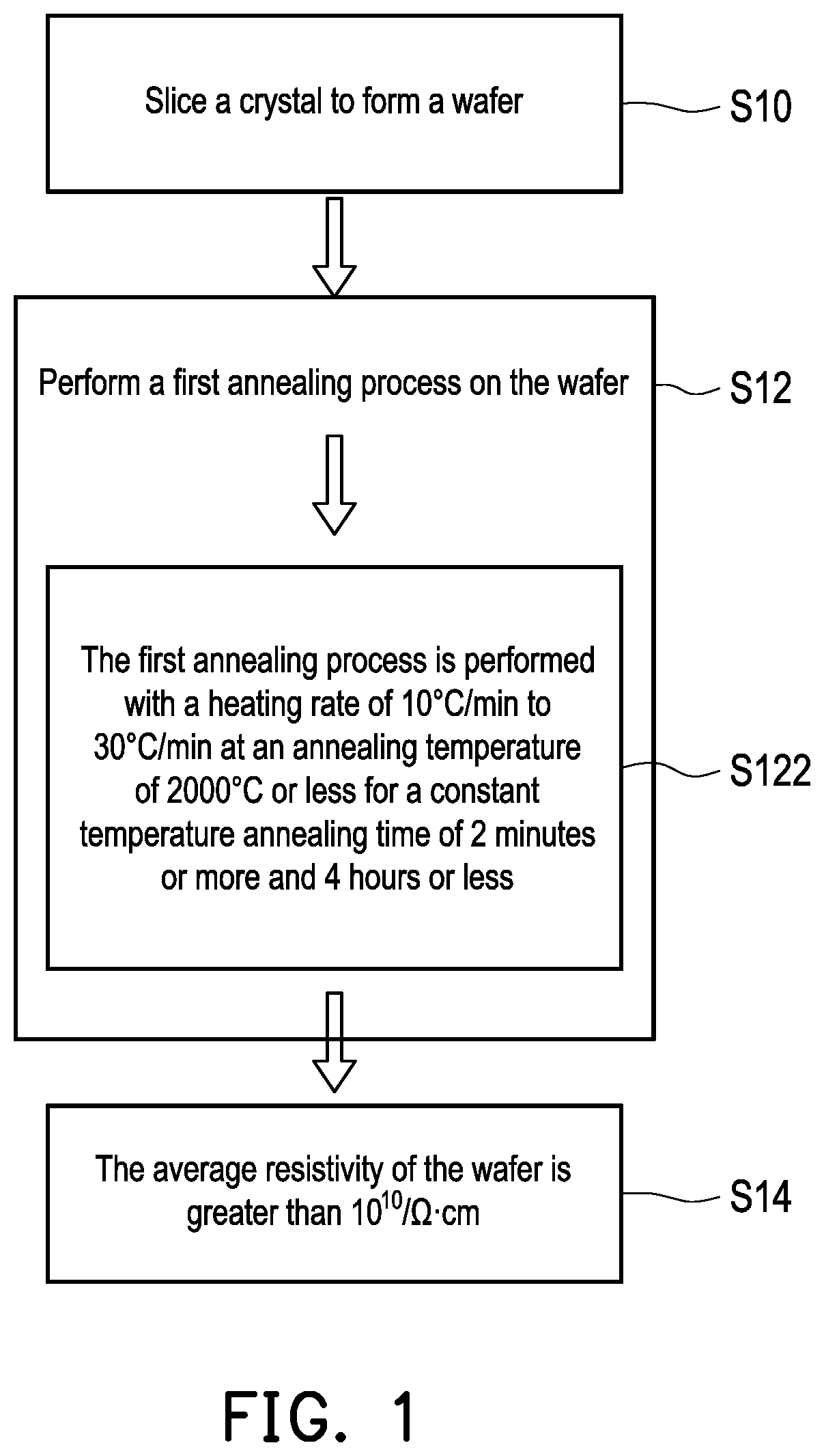
is a flowchart of a method of fabricating a silicon carbide material according to an embodiment of the disclosure.
A to C are schematic cross-sectional views of the method of fabricating the silicon carbide material according to some embodiments of the disclosure.
is a flowchart of a method of fabricating a silicon carbide material according to another embodiment of the disclosure.
A to C are schematic cross-sectional views of the method of fabricating the silicon carbide material according to some embodiments of the disclosure.
A to C are schematic cross-sectional views of the method of fabricating the silicon carbide material according to some embodiments of the disclosure.
DESCRIPTION OF THE EMBODIMENTS
is a flowchart of a method of fabricating a silicon carbide material according to an embodiment of the disclosure. A to C are schematic cross-sectional views of the method of fabricating the silicon carbide material according to some embodiments of the disclosure. Hereinafter, the method of fabricating the silicon carbide material of the embodiment of the disclosure will be described below with reference to the steps in and the schematic cross-sectional views of A to C .
Referring to step S 10 of and A and B , a crystal 100 obtained through a crystal growth process is sliced to form a wafer. As shown in A , the crystal 100 may be formed through a conventional crystal growth process. In some embodiments, the crystal 100 or an ingot may be formed through a physical vapor transport method via induction heating in a high-temperature furnace to volatilize a silicon carbide solid raw material for depositing on a seed crystal surface for growing and thickening. The crystal 100 or ingot may have different crystal structures depending on a manufacturing method, a manufacturing material, and a crystal orientation of the seed crystal. For example, silicon carbide crystals/ingots include 4H-silicon carbide, 6H-silicon carbide, etc. 4H-silicon carbide and 6H-silicon carbide belong to a hexagonal crystal system. In some embodiments, the crystal 100 includes a first surface 100 A and a second surface 100 B opposite to the first surface 100 A. The first surface 100 A is, for example, a carbon surface, and the second surface 100 B is, for example, a silicon surface.
As shown in B , after the growth of the crystal 100 is completed, the crystal 100 is sliced. For example, sides and corners of the crystal 100 are cut along a first direction D 1 to obtain an equal-diameter cylinder, and then the crystal 100 is ground into round corners to prevent sides and corners of the crystal 100 from being broken due to collision. Then, the crystal 100 is sliced along a second direction D 2 to obtain a plurality of wafers. The slicing method of the crystal 100 includes slicing with a knife or a steel wire in collaboration with abrasive particles (abrasive particles such as diamond particles). After the crystal 100 is sliced and ground and polished, a plurality of silicon carbide wafers 100 W as shown in C may be obtained.
Then, referring to step S 12 of and as shown in C , a first annealing process AN 1 is performed on the silicon carbide wafer 100 W. In some embodiments, conditions of the first annealing process AN 1 include performing step S 122 . To be specific, step S 122 includes adopting a heating rate of 10° C./min to 30° C./min, an annealing temperature of 2000° C. or less, and a constant temperature annealing time of 2 minutes or more and 4 hours or less for performing the first annealing process AN 1 . In this way, after performing the first annealing process AN 1 , as shown by step S 14 of and as shown in C , an average resistivity of the silicon carbide wafer 100 W is greater than 10 10 Ω·cm.
is a flowchart of a method of fabricating a silicon carbide material according to another embodiment of the disclosure. A to C are schematic cross-sectional views of the method of fabricating the silicon carbide material according to some embodiments of the disclosure. A to C are schematic cross-sectional views of the method of fabricating the silicon carbide material according to some embodiments of the disclosure. Hereinafter, the method of fabricating the silicon carbide material of the embodiment of the disclosure will be described below with reference to the steps in and the schematic cross-sectional views of A to C or A to C .
As shown in step S 20 of and A and A , the first annealing process AN 1 is performed on the crystal 100 obtained through the crystal growth process. The crystal 100 shown in A and A may be obtained, for example, by a similar manufacturing process to that of the crystal 100 shown in A , so that details thereof are not repeated. In some embodiments, conditions of the first annealing process AN 1 include performing step S 202 . To be specific, step S 202 includes adopting a heating rate of 10° C./min to 30° C./min, an annealing temperature of 2000° C. or less, and a constant temperature annealing time of 2 minutes or more and 4 hours or less for performing the first annealing process AN 1 .
In some embodiments, after performing the first annealing process AN 1 , as shown by step S 22 of , it is determined whether an average resistivity of the crystal 100 is greater than 10 10 Ω·cm. If the average resistivity of the crystal 100 is greater than 10 10 Ω·cm, the crystal 100 may be sliced directly as shown in B to obtain a plurality of wafers. After the crystal 100 is sliced and ground and polished, a plurality of silicon carbide wafers 100 W as shown in C may be obtained. In this way, as shown in step S 24 of and C , the average resistivity of the silicon carbide wafer 100 W formed after slicing may also be greater than 10 10 Ω·cm.
In some other embodiments, if it is determined in step S 22 that the average resistivity of the crystal 100 after the first annealing process AN 1 still cannot satisfy the range of greater than 10 10 Ω·cm, as shown in step S 26 of and B and C , after grinding and polishing the wafer 100 W formed after slicing, a second annealing process AN 2 is performed. For example, as shown in B , the crystal 100 is sliced to obtain a plurality of wafers. After the crystal 100 is sliced and ground and polished, a plurality of silicon carbide wafers 100 W as shown in C may be obtained. Then, the second annealing process AN 2 is performed on the silicon carbide wafers 100 W.
In some embodiments, the conditions of the second annealing process AN 2 include: a heating rate of 10° C./min to 30° C./min, an annealing temperature of 2000° C. or less, and a constant temperature annealing time of 2 minutes or more and 4 hours or less for performing the second annealing process AN 2 . In this way, as shown in step S 28 of and C , the average resistivity of the silicon carbide wafer 100 W obtained after performing the second annealing process AN 2 may be greater than 10 10 Ω·cm.
In the aforementioned embodiment, regardless of the first annealing process AN 1 or the second annealing process AN 2 , the annealing temperature is below 2000° C., and for example, is in an annealing temperature range of 1950° C. to 2000° C. In some preferred embodiments, the annealing temperature is in the range of 1950° C. to 1980° C. In addition, the constant temperature annealing time is 2 minutes or more and 4 hours or less, and is preferably 10 minutes or more and 3 hours or less, and most preferably 30 minutes or more and 2 hours or less. In this way, when the annealing temperature and the constant temperature annealing time are controlled within the above ranges, the resistivity of the crystal/wafer may be improved while avoiding the quality deterioration or cracking of the crystal/wafer.
In addition, in the aforementioned embodiment, regardless of the first annealing process AN 1 or the second annealing process AN 2 , the heating rate thereof is controlled within the range of 10° C./min to 30° C./min. For example, in some embodiments, when the heating rate is within a range of 25° C./min to 30° C./min, the part of the obtained wafer 100 W or the crystal 100 with the average resistivity greater than 5*10 11 Ω·cm occupies 100% of an area of the wafer 100 W or the crystal 100 . In some embodiments, when the heating rate is within a range of 22° C./min to 26° C./min, the part of the obtained wafer 100 W or the crystal 100 with the average resistivity greater than 10 11 Ω·cm occupies 100% of the area of the wafer 100 W or the crystal 100 . In some embodiments, when the heating rate is within a range of 20° C./min to 24° C./min, the part of the obtained wafer 100 W or the crystal 100 with the average resistivity greater than 5*10 10 Ω·cm occupies 100% of the area of the wafer 100 W or the crystal 100 . In some embodiments, when the heating rate is within a range of 10° C./min to 20° C./min, the part of the obtained wafer 100 W or the crystal 100 with the average resistivity greater than 10 10 Ω·cm occupies 100% of the area of the wafer 100 W or the crystal 100 .
In this way, when the heating rate is controlled within the above range, the resistivity of the crystal/wafer may be increased while avoiding the quality deterioration or cracking of the crystal/wafer.
In order to prove that the fabrication method of the silicon carbide wafer of the disclosure may simultaneously increase the resistivity of the wafer and avoid quality deterioration or cracking of the wafer, following experimental examples are provided below for description.
Experimental Example A
In the following experimental example, the annealing process of the disclosure is performed on the wafer formed after slicing, and the average resistivity thereof is determined. Where, the annealing temperature is controlled to 1950° C., the constant temperature annealing time is 30 minutes, and the heating rate is adjusted to the range of 10° C./min to 30° C./min. Through the adjustment of the heating rate, the average resistivity of the wafer is as shown in table 1.
TABLE 1
Group
Experimental example Experimental example Experimental example Experimental
A1 A2 A3 example A4
Heating Percentage: Heating Percentage: Heating Percentage: Heating Percentage:
rate resistivity rate resistivity rate resistivity rate resistivity
(° C./min) range X % (° C./min) range X % (° C./min) range X % (° C./min) range X %
10-20 the part with 20-24 the part with 22-26 the part with 25-30 the part with
average average average average
resistivity resistivity resistivity resistivity
greater than greater than greater than greater than
10 10 Ω · cm 5*10 10 Ω · cm 10 11 Ω · cm 5*10 11 Ω · cm
occupies 80% occupies 80% occupies 80% occupies 80%
of the area of of the area of of the area of of the area of
the wafer the wafer the wafer the wafer
10-18 the part with 20-23 the part with 22-25 the part with 25-29 the part with
average average average average
resistivity resistivity resistivity resistivity
greater than greater than greater than greater than
10 10 Ω · cm 5*10 10 Ω · cm 10 11 Ω · cm 5*10 11 Ω · cm
occupies 90% occupies 90% occupies 90% occupies 90%
of the area of of the area of of the area of of the area of
the wafer the wafer the wafer the wafer
10-16 the part with 20-22 the part with 22-24 the part with 25-27 the part with
average average average average
resistivity resistivity resistivity resistivity
greater than greater than greater than greater than
10 10 Ω · cm 5*10 10 Ω · cm 10 11 Ω · cm 5*10 11 Ω · cm
occupies occupies occupies occupies
100% of the 100% of the 100% of the 100% of the
area of the area of the area of the area of the
wafer wafer wafer wafer
From the experimental examples in table 1 above, it may be confirmed that when the annealing process of the disclosure is used to fabricate the silicon carbide wafers, the average resistivity of the wafers may be effectively controlled to a range greater than 10 10 Ω·cm. As shown in the experimental example A1, when the heating rate is adjusted within the range of 10° C./min to 20° C./min, the part of the silicon carbide wafer with the average resistivity greater than 10 10 Ω·cm may occupy 80% to 100% of the entire wafer area. As shown in the experimental example A2, when the heating rate is adjusted within the range of 20° C./min to 24° C./min, the part of the silicon carbide wafer with the average resistivity greater than 5*10 10 Ω·cm may occupy 80% to 100% of the entire wafer area. As shown in the experimental example A3, when the heating rate is adjusted within the range of 22° C./min to 26° C./min, the part of the silicon carbide wafer with the average resistivity greater than 10 11 Ω·cm may occupy 80% to 100% of the entire wafer area. As shown in the experimental example A4, when the heating rate is adjusted within the range of 25° C./min to 30° C./min, the part of the silicon carbide wafer with the average resistivity greater than 5*10 11 Ω·cm may occupy 80% to 100% of the entire wafer area.
Experimental Example B
In order to further confirm the correlation between the annealing temperature and the resistivity of the wafer/crystal with the quality thereof, in this experimental example, the annealing process of the disclosure is performed to the crystal. Where, the constant temperature annealing time is 30 minutes, the heating rate is 10° C./min, and the annealing temperature is controlled at 1950° C., 2000° C. or 2050° C. The experimental results are shown in table 2.
TABLE 2
Quality/ Experimental Experimental Experimental Experimental
temperature example B1 example B2 example B3 example B4
Annealing 1850° C. 1950° C. 2000° C. 2050° C.
temperature
Crystal 0% 0% 5% 20%
damage
rate (%)
(The surface
becomes
black due to
carbonization)
Resistivity Poor Good Good Poor
From the experimental results in table 2, it may be known that when the annealing temperatures (experimental examples B2 and B3) of the disclosure are used to perform the annealing process, the crystal may achieve better resistivity (10 10 Ω·cm or more), and meanwhile avoiding the problem of crystal damage. As shown in experimental example B2 in table 2, when the annealing temperature is controlled at 1950° C., the crystal is not damaged, and the resistivity is good (10 10 Ω·cm or more). In addition, as shown in experimental example B3 in table 2, when the annealing temperature is controlled at 2000° C., the crystal is slightly damaged, but the resistivity is still maintained good (10 10 Ω·cm or more).
In contrast, as shown in experimental example B1 in table 2, when the annealing temperature is controlled at 1850° C., the crystal cannot reach the ideal resistivity (below 10 10 Ω·cm) due to that the annealing temperature is too low. In addition, as shown in experimental example B4 in table 2, when the annealing temperature is controlled at 2050° C., since the heating rate is slower than that of the a conventional method, the higher annealing temperature increases the risk of crystal damage. Therefore, the surface of the crystal will be blackened and damaged due to carbonization, which may worsen the resistivity (below 10 10 Ω·cm).
Experimental Example C
In order to further confirm the correlation between the heating rate and the resistivity of the wafer/crystal, in this experimental example, the annealing process of the disclosure is performed to the wafer. Where, the annealing temperature is controlled at 1950° C., the constant temperature annealing time is 30 minutes, and the heating rate is adjusted to the range of 10° C./min to 40° C./min. The experimental results are shown in table 3.
TABLE 3
Experimental Experimental Experimental Experimental
example C1 example C2 example C3 example C4
Heating rate 10° C./min 20° C./min 30° C./min 40° C./min
Resistivity Good Good Good Poor
From the experimental results in table 3, it is learned that when the heating rates of the disclosure (experimental examples C1-C3) are used to perform the annealing process, the wafer may reach better resistivity (above 10 10 Ω·cm). In contrast, as shown in experimental example C4 in table 3, when the heating rate is adjusted to a range of 40° C./min which is outside the limit of the disclosure, the resistivity will be worsen (10 10 Ω·cm or less).
In summary, by adopting the fabrication method of the silicon carbide material of the embodiment of the disclosure, atoms in the silicon carbide material may be arranged more orderly, and the resistivity of the wafer/crystal may be improved. In addition, by reducing the annealing temperature and the heating rate of the annealing process, and controlling the annealing temperature and the heating rate within certain ranges, the resistivity may be increased while avoiding the quality deterioration or cracking of the crystal/wafer.
Figures (5)
Citations
This patent cites (6)
- US6436361
- US2003/0233975
- US109234802
- US109338463
- US109338463
- US20160049432