Abstract
A display device includes a pixel circuit disposed on a substrate, and a display element on the pixel circuit. The pixel circuit includes a first thin-film transistor comprising a first semiconductor layer and a first gate electrode insulated from the first semiconductor layer, a second thin-film transistor comprising a second semiconductor layer and a second gate electrode insulated from the second semiconductor layer, the second semiconductor layer being connected to the first semiconductor layer and the first gate electrode, a first shielding layer overlapping the second semiconductor layer, and a second shielding layer overlapping the second semiconductor layer and stacked on the first shielding layer.
Claims (22)
1 . An electronic device comprising: a display panel; and a window on the display panel, wherein the display panel comprises: a first transistor including a first semiconductor layer, a first gate electrode and a second gate electrode; a first shielding layer overlapping a portion of the first semiconductor layer, in a plan view; a capacitor including a first capacitor electrode and a second capacitor electrode on the first capacitor electrode; and a connection electrode connected to the first capacitor electrode and the first semiconductor layer, wherein the first semiconductor layer comprises a source area, a drain area, a first channel area, a second channel area and a middle area, the middle area is between the first channel area and the second channel area, wherein the first gate electrode overlaps the first channel area and the second gate electrode overlaps the second channel area in the plan view, wherein the first shielding layer overlaps the middle area of the first semiconductor layer, and wherein the connection electrode is connected to one of the source area and the drain area of the first semiconductor layer.
Show 21 dependent claims
2 . The electronic device of claim 1 , wherein the first gate electrode and the second gate electrode are in a same layer.
3 . The electronic device of claim 1 , wherein the connection electrode is connected to the first capacitor electrode through an opening defined in the second capacitor electrode.
4 . The electronic device of claim 1 , further comprising: a driving transistor, wherein a part of the first capacitor electrode is a gate electrode of the driving transistor.
5 . The electronic device of claim 4 , wherein a semiconductor layer of the driving transistor is connected to the other one of the source area and the drain area of the first semiconductor layer.
6 . The electronic device of claim 4 , further comprising: a second transistor including a second semiconductor layer, a first gate electrode and a second gate electrode, wherein the second semiconductor layer comprises a source area, a drain area, a first channel area, a second channel area, and a middle area, wherein the middle area is between the first channel area and the second channel area, wherein the first gate electrode of the second transistor overlaps the first channel area of the second semiconductor layer and the second gate electrode of the second transistor overlaps the second channel area of the second semiconductor layer in a plan view, and wherein the connection electrode is connected to one of the source area and the drain area of the second semiconductor layer.
7 . The electronic device of claim 6 , further comprising: a first voltage line connected to the other one of the source area and the drain area of the second semiconductor layer.
8 . The electronic device of claim 1 , wherein the first shielding layer and the second capacitor electrode are on a same layer.
9 . The electronic device of claim 1 , further comprising: a second voltage line connected to the first shielding layer.
10 . The electronic device of claim 9 , further comprising: a second shielding layer overlapping the first shielding layer.
11 . The electronic device of claim 10 , wherein the second shielding layer is connected to the first shielding layer.
12 . The electronic device of claim 10 , wherein a part of the second voltage line is the second shielding layer.
13 . The electronic device of claim 10 , wherein the connection electrode and the second shielding layer are on a same layer.
14 . The electronic device of claim 1 , further comprising: a voltage line connected to the second capacitor electrode.
15 . The electronic device of claim 14 , wherein a voltage applied to the first shielding layer and a voltage applied to the voltage line are the same.
16 . The electronic device of claim 1 , wherein the first semiconductor layer of the first transistor comprises polysilicon.
17 . The electronic device of claim 1 , wherein the first shielding layer receives a constant voltage.
18 . The electronic device of claim 1 , further comprising: a scan line providing a scan signal to the first gate electrode and the second gate electrode of the first transistor, wherein the scan line crosses the connection electrode.
19 . The electronic device of claim 18 , wherein the scan line is in a space between the first shielding layer and the second capacitor electrode in the plan view.
20 . The electronic device of claim 1 , wherein the electronic device is one of a smartphone, a mobile phone, a smart watch, a navigation device, a game console, a television (TV), a head unit for a vehicle, a notebook computer, a laptop computer, a tablet computer, a personal media player (PMP), and a personal digital assistant (PDA).
21 . The electronic device of claim 1 , further comprising: an optical functional layer between the display panel and the window.
22 . The electronic device of claim 1 , wherein the electronic device is a flexible device.
Full Description
Show full text →
CROSS-REFERENCE TO RELATED APPLICATION
This application is a continuation of U.S. application Ser. No. 18/592,891 filed on Mar. 1, 2024, which is a continuation of U.S. application Ser. No. 18/161,434 filed on Jan. 30, 2023, issued as U.S. Pat. No. 11,950,460 issued on Apr. 2, 2024, which is a continuation of U.S. application Ser. No. 17/085,288 filed on Oct. 30, 2020, issued as U.S. Pat. No. 11,569,327 issued on Jan. 31, 2023, which claims priority under 35 U.S.C. § 119 to Korean Patent Application No. 10-2019-0160007, filed on Dec. 4, 2019, in the Korean Intellectual Property Office, the disclosure of each of which is herein incorporated by reference in its entirety.
BACKGROUND
1. Field
The present invention relates to a display device, and more particularly, to a display device including a thin-film transistor with a shielding layer.
2. Description of Related Art
In general, display devices include a display element and a driving circuit for controlling electrical signals to be applied to the display element. The driving circuit includes a thin-film transistor (TFT), a storage capacitor, and a plurality of signal lines.
To precisely control whether the display element emits light and a degree of emission of the display element, the number of TFTs to be electrically connected to one display element has increased. Thus, research into a way to solve the problem relating to high integration and power consumption of the display devices is briskly under way.
SUMMARY
One or more embodiments include a display device having enhanced display quality. However, this objective is just an example, and the scope of the present disclosure is not limited thereby.
Additional aspects will be set forth in part in the description which follows and, in part, will be apparent from the description, or may be learned by practice of the presented embodiments of the disclosure.
According to an exemplary embodiment of the present invention, a display device includes a pixel circuit disposed on a substrate, and a display element on the pixel circuit. The pixel circuit includes a first thin-film transistor comprising a first semiconductor layer and a first gate electrode insulated from the first semiconductor layer, a second thin-film transistor comprising a second semiconductor layer and a second gate electrode insulated from the second semiconductor layer, a first end of the second semiconductor layer being connected to a first end of the first semiconductor layer and a second end of the second semiconductor layer being connected to the first gate electrode, a first shielding layer overlapping the second semiconductor layer, and a second shielding layer overlapping the second semiconductor layer and stacked on the first shielding layer.
The second gate electrode includes a first sub gate electrode and a second sub gate electrode. The second semiconductor layer including a first channel area and a second channel area. The second gate electrode includes a first sub gate electrode overlapping the first channel area and a second sub gate electrode overlapping the second channel area. The second shielding layer overlaps a part between the first channel area and the second channel area.
The first sub gate electrode and the second sub gate electrode are located on the same layer.
The first shielding layer and the second shielding layer comprise the same material.
The first shielding layer and the second shielding layer comprise different materials from each other.
The pixel circuit further includes a capacitor including an upper electrode and a part of the first gate electrode as a lower electrode, and a power supply voltage line connected to the upper electrode. The upper electrode overlaps the part of the first gate electrode.
The first shielding layer, the second shielding layer and the upper electrode comprise the same material. The second shielding layer is a part of the power supply voltage line. The first shielding layer is connected to the power supply voltage line.
The first shielding layer and the upper electrode comprise the same material. The second shielding layer and the power supply voltage line comprise the same material.
The pixel circuit further includes a capacitor including an upper electrode and a part of the first gate electrode as a lower electrode, a power supply voltage line connected to the upper electrode, and a third shielding layer stacked on the second shielding layer. The second shielding layer is interposed between the first shielding layer and the third shielding layer. The upper electrode and the first shielding layer are located on the same layer. The upper electrode overlaps the part of the first gate electrode. The power supply voltage line and the second shielding layer are located on the same layer. The third shielding layer overlaps the second semiconductor layer.
The display device further includes a data line connected to the pixel circuit. The data line and the third shielding layer are located on the same layer.
The first shielding layer and the upper electrode comprises the same material. The second shielding layer and the power supply voltage line comprise the same material. The third shielding layer and the data line comprise the same material.
The third shielding layer is connected to the power supply voltage line.
According to an exemplary embodiment of the present invention, a display device includes a pixel circuit disposed on a substrate and a display element on the pixel circuit. The pixel circuit includes a thin-film transistor comprising a semiconductor layer comprising a first channel area and a second channel area, a first sub gate electrode overlapping the first channel area and a second sub gate electrode overlapping the second channel area. The pixel circuit further include a first shielding layer overlapping a part between the first channel area and the second channel area, and a second shielding layer stacked on the first shielding layer.
The first shielding layer and the second shielding layer comprise the same material.
The first shielding layer and the second shielding layer comprise different materials from each other.
The pixel circuit further includes a capacitor comprising a lower electrode and an upper electrode and a power supply voltage line is electrically connected to the upper electrode of the capacitor. The lower electrode, the first sub gate electrode and the sub second gate electrode are located on the same layer. The upper electrode overlaps the lower electrode. The first shielding layer and the upper electrode of the capacitor comprise the same material. The second shielding layer and the power supply voltage line comprises the same material.
The second shielding layer is a part of the power supply voltage line. The first shielding layer is connected to the power supply voltage line.
The pixel circuit further includes a third shielding layer located on the second shielding layer. The third shielding layer overlaps part between the first channel area and the second channel area.
The pixel circuit further includes a data line connected to the pixel circuit. The data line and the third shielding layer are located on the same layer.
BRIEF DESCRIPTION OF THE DRAWINGS
The above and other aspects, features, and advantages of certain embodiments of the disclosure will be more apparent from the following description taken in conjunction with the accompanying drawings, in which:
is a perspective view schematically illustrating a display device according to an exemplary embodiment;
is a cross-sectional view schematically illustrating a display device according to an exemplary embodiment;
is a plan view schematically illustrating a display panel according to an exemplary embodiment;
is a cross-sectional view schematically illustrating one pixel of a display panel according to an exemplary embodiment;
is a schematic layout diagram of a plurality of pixels of a display device according to an exemplary embodiment;
is an equivalent circuit diagram schematically illustrating a pixel circuit of one pixel of a display panel according to an exemplary embodiment;
A through 7 D are cross-sectional views schematically illustrating a thin-film transistor according to an exemplary embodiment;
is a layout diagram illustrating locations of a plurality of thin-film transistors and a capacitor arranged in pixel circuits of a display device according to an exemplary embodiment;
A and 9 B are enlarged views of a region including a third thin-film transistor of according to an exemplary embodiment;
is a schematic cross-sectional view of the display device cut along line II-II′ of according to an exemplary embodiment; and
is a schematic cross-sectional view of the display device cut along line III-III′ of according to an exemplary embodiment.
DETAILED DESCRIPTION OF EXEMPLARY EMBODIMENTS
Reference will now be made in detail to embodiments, examples of which are illustrated in the accompanying drawings, wherein like reference numerals refer to like elements throughout. In this regard, the present embodiments may have different forms and should not be construed as being limited to the descriptions set forth herein. Accordingly, the embodiments are merely described below, by referring to the figures, to explain aspects of the present description. As used herein, the term “and/or” includes any and all combinations of one or more of the associated listed items. Throughout the disclosure, the expression “at least one of a, b or c” indicates only a, only b, only c, both a and b, both a and c, both b and c, all of a, b, and c, or variations thereof.
Hereinafter, embodiments of the present disclosure will be described below in more detail with reference to the accompanying drawings. Those elements that are the same or are in correspondence are rendered the same reference numeral regardless of the figure number, and a redundant description therewith is omitted.
It will be understood that although the terms “first,” “second,” etc. may be used herein to describe various elements, these elements should not be limited by these terms. These elements are only used to distinguish one element from another.
As used herein, the singular forms “a,” “an” and “the” are intended to include the plural forms as well, unless the context clearly indicates otherwise.
It will be further understood that the terms “comprises” and/or “comprising” used herein specify the presence of stated features or elements, but do not preclude the presence or addition of one or more other features or elements.
It will be understood that when a layer, region, or element is referred to as being “formed on,” another layer, region, or element, it may be directly or indirectly formed on the other layer, region, or element. That is, for example, intervening layers, regions, or elements may be present.
Sizes of elements in the drawings may be exaggerated or reduced for convenience of explanation. In other words, since sizes and thicknesses of components in the drawings are arbitrarily illustrated for convenience of explanation, the following embodiments are not limited thereto.
When a certain embodiment may be implemented differently, a specific process order may be performed differently from the described order. For example, two consecutively described processes may be performed substantially at the same time or performed in an order opposite to the described order.
In the present specification, “A and/or B” represents A, B, or A and B. “At least one of A and B” represents A, B, or A and B.
It will be understood that when a layer, region, or element is referred to as being “connected to,” another layer, region, or element, it may be directly or indirectly connected to the other layer, region, or element. That is, for example, intervening layers, regions, or elements may be present. For example, it will be understood that when a layer, region, or element is referred to as being “electrically connected to,” another layer, region, or element, it may be directly or indirectly electrically connected to the other layer, region, or element. That is, for example, intervening layers, regions, or elements may be present.
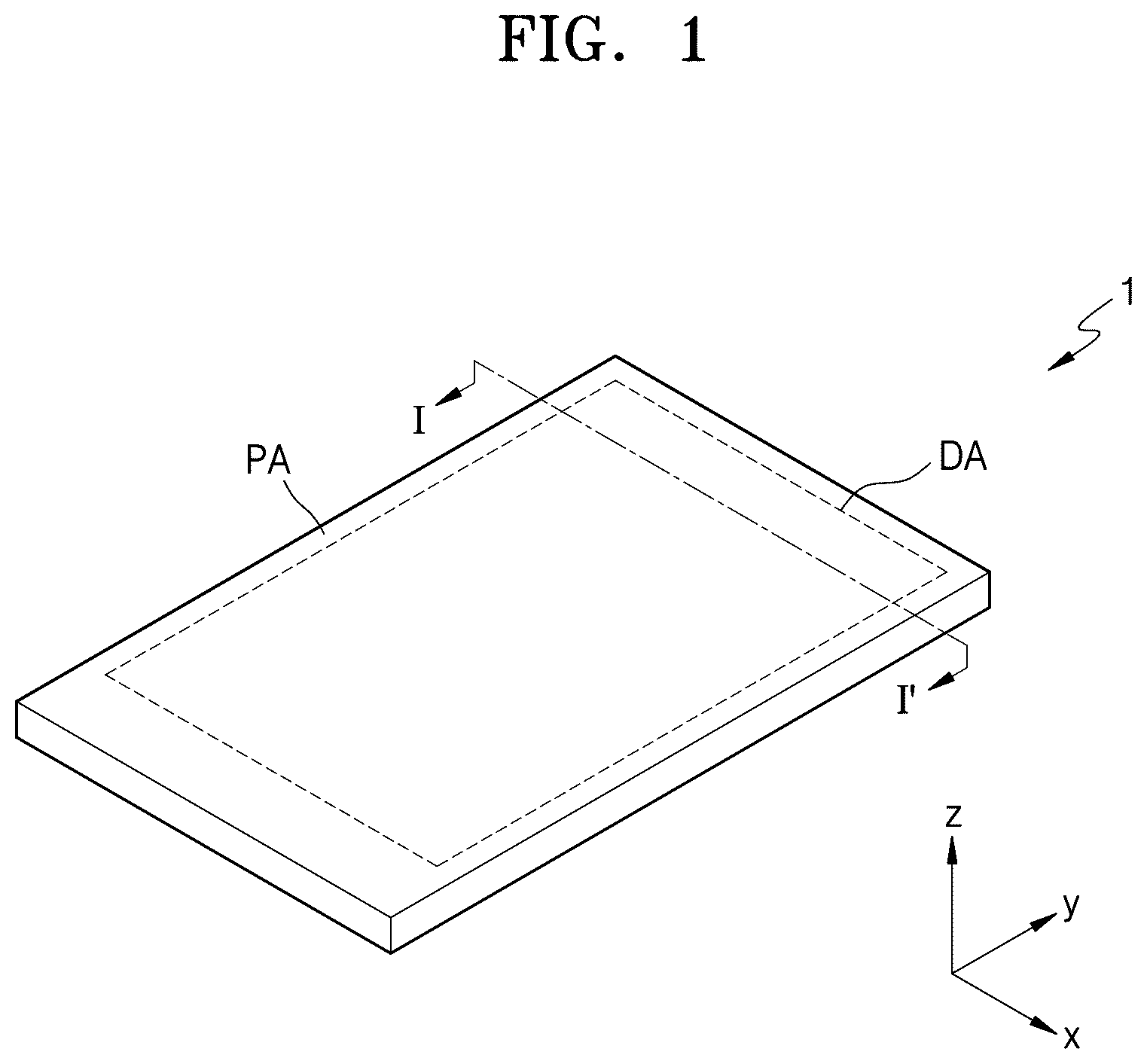
is a perspective view schematically illustrating a display device according to an exemplary embodiment. is a cross-sectional view schematically illustrating a display device according to an exemplary embodiment, which corresponds to a cross-section cut along line I-I′ of .
A display device according to one or more exemplary embodiments may be implemented with an electronic device, such as a smartphone, a mobile phone, a smart watch, a navigation device, a game console, a television (TV), a head unit for a vehicle, a notebook computer, a laptop computer, a tablet computer, a personal media player (PMP), or a personal digital assistant (PDA). Also, the electronic device may be a flexible device.
A display device 1 may include a display area DA, in which an image is displayed, and a peripheral area PA around the display area DA. The display device 1 may provide a certain image using light emitted from a plurality of pixels arranged in the display area DA.
In a plane view of the display area DA, the display area DA may have a rectangular shape, as shown in . The present invention is not limited thereto. In an exemplary embodiment, the display area DA may have a polygonal shape, such as a triangular, pentagonal, or hexagonal shape, or an atypical shape, such as a circular or an oval shape.
The peripheral area PA around the display area DA may be a kind of non-display area in which no pixels are arranged. In an exemplary embodiment, the peripheral area PA may be a pixel-free area. The display area DA may be entirely surrounded by the peripheral area PA. A variety of signal lines for providing electrical signals to the display area DA and pads to which a printed circuit board (PCB) or a driver integrated circuit (IC) chip is to be attached, may be arranged in the peripheral area PA.
Hereinafter, an organic light-emitting display device will be described as an example of the display device 1 according to an exemplary embodiment. However, a display device according to the present disclosure is not limited thereto. In an exemplary embodiment, examples of the display device 1 according to the present disclosure may include an inorganic light-emitting display device, an inorganic electroluminescence (EL) display device, or a quantum dot light-emitting display device.
Referring to , the display device 1 may include a display panel 10 , an input sensing layer 40 located on the display panel 10 , an optical functional layer 50 , and a window 60 . The window 60 may cover the optical functional layer 50 .
The display panel 10 may display an image. The display panel 10 includes pixels arranged in the display area DA. The pixels may include a display element. The display element may be connected to a pixel circuit. The display element may include an organic light-emitting diode or a quantum organic light-emitting diode.
The input sensing layer 40 may be configured to obtain coordinate information according to an external input, for example, a touch event. The input sensing layer 40 may include a sensing electrode or touch electrode and trace lines connected to the sensing electrode. The input sensing layer 40 may be located on the display panel 10 . The input sensing layer 40 may be configured to sense an external input by using a mutual capacitance method and/or a self-capacitance method.
The input sensing layer 40 may be formed directly on the display panel 10 or may be formed separately from the display panel 10 and then may be coupled to the display panel 10 by using an adhesive layer, such as an optical clear adhesive. For example, the input sensing layer 40 may be consecutively formed after a process of forming the display panel 10 is performed. In this case, the input sensing layer 40 may be part of the display panel 10 , and no adhesive layer may be between the input sensing layer 40 and the display panel 10 . In , the input sensing layer 40 is between the display panel 10 and the optical functional layer 50 . However, the present invention is not limited thereto. In an exemplary embodiment, the input sensing layer 40 may be located on the optical functional layer 50 .
The optical functional layer 50 may include an antireflective layer. The antireflective layer may be configured to reduce reflectivity of light (external light) incident onto the display panel 10 from the outside through the window 60 . The antireflective layer may include a phase retarder and a polarizer. The phase retarder may be of a film type or liquid crystal coating type and may include a λ/2 phase retarder and/or a λ/4 phase retarder. The polarizer may also be of a film type or liquid crystal coating type. The film type may include an elongation-type synthetic resin film, and the liquid crystal coating type may include liquid crystals arranged in a certain arrangement. The phase retarder and the polarizer may further include a protective film. The phase retarder and the polarizer itself or the protective film may be defined as a base layer for the antireflective layer.
In an exemplary embodiment, the antireflective layer may include a black matrix and color filters. The color filters may be arranged considering colors of light emitted from each of the pixels of the display panel 10 . In another embodiment, the antireflective layer may include a destructive interference structure. The destructive interference structure may include a first reflective layer and a second reflective layer, which are located on different layers. First reflected light and second reflected light reflected from the first reflective layer and the second reflective layer, respectively, may destructively interfere. Thus, the reflectivity of external light may be reduced.
The optical functional layer 50 may include a lens layer. The lens layer may be configured to increase emission efficiency of light emitted from the display panel 10 or to reduce color deviation. The lens layer may include a layer having a concave or convex lens shape or/and a plurality of layers having different refractive indices. The optical functional layer 50 may include both the antireflective layer and the lens layer described above or one thereof.
In an exemplary embodiment, the optical functional layer 50 may be consecutively formed after a process of forming the display panel 10 and/or the input sensing layer 40 is performed. In this case, no adhesive layer may be between the optical functional layer 50 and the display panel 10 and/or the input sensing layer 40 .
is a plan view schematically illustrating a display panel according to an exemplary embodiment. is a cross-sectional view schematically illustrating one pixel of a display panel according to an exemplary embodiment. For convenience of description and clarity of drawings, a thin film encapsulation layer that is an encapsulation member is omitted in .
Referring to , the display panel 10 may include a display area DA and a peripheral area PA. illustrates a substrate 100 of the display panel 10 . For example, the substrate 100 may have a first region corresponding to the display area DA and a second region corresponding to the peripheral area PA.
The substrate 100 may include various materials, such as glass, metal, or plastic. In an embodiment, the substrate 100 may include a flexible material. Here, the flexible material refers to a substrate that is bendable, foldable, or rollable. The substrate 100 made of the flexible material may include ultra-thin glass, metal, or plastic.
The display panel 10 includes a plurality of pixels P arranged in the display area DA. Each of the pixels P may include an organic light-emitting diode OLED that is a display element, as shown in . The organic light-emitting diode OLED may be connected to a pixel circuit. The pixel circuit may include a plurality of transistors and a capacitor. Each of the pixels P may emit red, green, blue, or white light, for example, from the organic light-emitting diode OLED.
The organic light-emitting diode OLED may include a pixel electrode 221 , an opposite electrode 223 spaced apart from the pixel electrode 221 , and an intermediate layer 222 between the pixel electrode 221 and the opposite electrode 223 .
The pixel electrode 221 is located on a planarization layer PNL. The pixel electrode 221 may include a conductive oxide such as indium tin oxide (ITO), indium zinc oxide (IZO), zinc oxide (ZnO), indium oxide (In 2 O 3 ), indium gallium oxide (IGO), or aluminum zinc oxide (AZO). In an exemplary embodiment, the pixel electrode 221 may include a reflective layer including silver (Ag), magnesium (Mg), aluminum (Al), platinum (Pt), palladium (Pd), gold (Au), nickel (Ni), neodymium (Nd), iridium (Ir), chromium (Cr), or a compound thereof. In an exemplary embodiment, the pixel electrode 221 may further include a layer including ITO, IZO, ZnO, or In 2 O 3 on/under the above-described reflective layer.
A pixel-defining layer PDL may be formed on the pixel electrode 221 . The pixel-defining layer PDL may include an opening OP for exposing a top surface of the pixel electrode 221 and may cover edges of the pixel electrode 221 . For example, the opening OP may extend through the pixel-defining layer PDL to expose the top surface of the pixel electrode 221 . The pixel-defining layer PDL may include an organic insulating material. In an exemplary embodiment, the pixel-defining layer PDL may include an organic insulating material or an inorganic insulating material. An emission area may be defined by the opening OP of the pixel-defining layer PDL. The emission area may be an area in which an emission layer 222 b is located.
The intermediate layer 222 may include the emission layer 222 b . The intermediate layer 222 may further include a first functional layer 222 a under the emission layer 222 b and/or a second functional layer 222 c on the emission layer 222 b . The emission layer 222 b may include a polymer or small molecular weight organic material that emits light of a certain color.
The first functional layer 222 a may have a single layer or multi-layer structure. For example, when the first functional layer 222 a includes a polymer material, the first functional layer 222 a that is a hole transport layer (HTL) having a single layer structure may include poly-(3,4)-ethylene-dihydroxy thiophene (PEDOT) or polyaniline (PANI). When the first functional layer 222 a includes a small molecular weight material, the first functional layer 222 a may include a hole injection layer (HIL) and an HTL.
The second functional layer 222 c may be omitted. For example, when the first functional layer 222 a and the emission layer 222 b include a polymer material, the second functional layer 222 c may be formed. The second functional layer 222 c may have a single layer or multi-layer structure. The second functional layer 222 c may include an electron transport layer (ETL) and/or an electron injection layer (EIL).
The emission layer 222 b of the intermediate layer 222 may be located in each pixel. For example, the emission layer 222 b may be patterned so as to correspond to the pixel electrode 221 . Each of the first functional layer 222 a and the second functional layer 222 c of the intermediate layer 222 , unlike in the emission layer 222 b , may be formed as a single body so as to correspond to the plurality of pixels P.
The opposite electrode 223 may include a conductive material having a small work function. For example, the opposite electrode 223 may include a (semi-) transparent layer including Ag, Mg, Al, Pt, Pd, Au, Ni, Nd, Ir, Cr, lithium (Li), calcium (Ca), or an alloy thereof. In an exemplary embodiment, the opposite electrode 223 may further include a layer, such as ITO, IZO, ZnO, or In 2 O 3 , on the (semi-) transparent layer including the above-described materials.
A capping layer 230 may be located on the opposite electrode 223 . For example, the capping layer 230 may include lithium fluoride (LiF) and may be formed by using thermal deposition. In some exemplary embodiments, the capping layer 230 may be omitted.
A scan driver 1100 for providing a scan signal to the pixel circuit connected to each pixel P, a data driver 1200 for providing a data signal to the pixel circuit connected to each pixel P, and main power supply lines (not shown) for providing a first power supply voltage and a second power supply voltage may be arranged in the peripheral area PA. In , the data driver 1200 is adjacent to one side of the substrate 100 . However, the present invention is not limited thereto. In an exemplary embodiment, the data driver 1200 may be arranged on a flexible printed circuit board (FPCB) electrically connected to a pad arranged at one side of the display panel 10 .
is a schematic layout diagram of a plurality of pixels in a display area of a display device according to an exemplary embodiment. The arrangement of pixels shown in may correspond to the arrangement of a plurality of pixels in an emission area. The emission area may be an area in which as shown in , an emission layer 222 b is located.
The display area DA may include a first pixel P 1 , a second pixel P 2 , and a third pixel P 3 , for example. The first pixel P 1 , the second pixel P 2 , and the third pixel P 3 may be repeatedly arranged in an x-direction (a first direction) and a y-direction (a second direction) according to certain patterns in the display area DA. Each of the first pixel P 1 , the second pixel P 2 , and the third pixel P 3 may include an organic light-emitting diode OLED. The organic light-emitting diode OLED of each pixel may be arranged on an upper layer of a pixel circuit. The organic light-emitting diode OLED may be located directly on an upper portion of the pixel circuit to overlap the pixel circuit or may be offset with the pixel circuit to overlap part of a pixel circuit of another pixel arranged in an adjacent row or column.
The first pixel P 1 may include a first emission area EA 1 , the second pixel P 2 may include a second emission area EA 2 , and a third pixel P 3 may include a third emission area EA 3 . An emission area of a pixel that is an area in which an emission layer is located, may be defined by an opening of a pixel-defining layer, as shown in .
The first emission area EA 1 of the first pixel P 1 and the third emission area EA 3 of the third pixel P 3 may be alternately arranged in odd columns in the y-direction. The second emission area EA 2 of the second pixel P 2 may be repeatedly arranged in even columns in the y-direction. In , it is assumed for the convenience of description that pixels are arranged in four columns 1 M to 4 M and two rows 1 N and 2 N. The arrangements of the pixels in the display area DA will be described with reference to the four columns 1 M to 4 M and the two rows 1 N and 2 N. For example, the first emission area EA 1 of the first pixel P 1 and the third emission area EA 3 of the third pixel P 3 may be alternately arranged in a first column 1 M and a third column 3 M in the y-direction. The second emission area EA 2 of the second pixel P 2 may be repeatedly arranged in a second column 2 M and a fourth column 4 M. The second column 2 M is between the first row 1 M and the third column 3 M. The third column 3 M is between the second column 2 M and the fourth column 4 M. The arrangement of the first emission area EA 1 of the first pixel P 1 and the third emission area EA 3 of the third pixel P 3 in the first column 1 M may be opposed to the arrangement of the first emission area EA 1 of the first pixel P 1 and the third emission area EA 3 of the third pixel P 3 in the third column 3 M.
The first emission area EA 1 of the first pixel P 1 and the third emission area EA 3 of the third pixel P 3 may be alternately arranged in a first sub-row 1 SN of each of rows 1 N and 2 N in the x-direction, and the second emission area EA 2 of the second pixel P 2 may be repeatedly arranged in a second sub-row 2 SN of each of the rows 1 N and 2 N in the x-direction. For example, the first emission area EA 1 of the first pixel P 1 , the second emission area EA 2 of the second pixel P 2 , the third emission area EA 3 of the third pixel P 3 , and the second emission area EA 2 of the second pixel P 2 may be repeatedly arranged in each of the rows 1 N and 2 N in a zigzag manner.
The first emission area EA 1 of the first pixel P 1 , the second emission area EA 2 of the second pixel P 2 , and the third emission area EA 3 of the third pixel P 3 may have different areas. In an exemplary embodiment, the third emission area EA 3 of the third pixel P 3 may have a greater area than that of the first emission area EA 1 of the first pixel P 1 . Also, the third emission area EA 3 of the third pixel P 3 may have a greater area than that of the second emission area EA 2 of the second pixel P 2 . The first emission area EA 1 of the first pixel P 1 may have a greater area than that of the second emission area EA 2 of the second pixel P 2 . However, the present invention is not limited thereto. In an exemplary embodiment, the third emission area EA 3 of the third pixel P 3 may have the same area as that of the first emission area EA 1 of the first pixel P 1 , and each of the first emission area EA 1 and the third emission area EA 3 may have an area greater than that of the second emission area EA 2 . In an exemplary embodiment, the first emission area EA 1 of the first pixel P 1 may have a greater area than that of the second emission area EA 2 of the second pixel P 2 and that of the third emission area EA 3 of the third pixel P 3 .
The first through third emission areas EA 1 , EA 2 , and EA 3 may have a polygonal shape, such as a rectangular or octagonal shape, a circular shape, or an oval shape. The polygonal shape may also include a vertex-rounded shape.
In an exemplary embodiment, as shown in , the first pixel P 1 may be a red pixel R that emits red light, the second pixel P 2 may be a green pixel G that emits green light, and the third pixel P 3 may be a blue pixel B that emits blue light. In an exemplary embodiment, the first pixel P 1 may be a red pixel R, the second pixel P 2 may be a blue pixel B, and the third pixel P 3 may be a green pixel G.
A pixel arrangement according to an exemplary embodiment is not limited to the arrangement described above. For example, the present disclosure may be applied to a pixel arrangement having a stripe arrangement, a mosaic arrangement, or a delta arrangement. Also, the present disclosure may also be applied to a pixel arrangement structure further including a white pixel for emitting white light.
is a circuit diagram schematically illustrating a pixel circuit of one pixel of a display panel according to an exemplary embodiment.
Referring to , a pixel circuit PC of a pixel P may include a plurality of first through seventh transistors T 1 through T 7 and a capacitor Cst. The first through seventh transistors T 1 through T 7 may be implemented with thin-film transistors.
The pixel P may be connected to a first scan line SL 1 for delivering a scan signal Sn, a second scan line SL 2 for delivering the previous scan signal Sn−1, a third scan line SL 3 for delivering the scan signal Sn, an emission control line EL for delivering an emission control signal En, and a data line DL for delivering a data signal Dm. The first scan line SL 1 and the third scan line SL 3 may be electrically connected to each other, and the same scan signal Sn may be applied to the first scan line SL 1 and the third scan line SL 3 .
The power supply voltage line PL may be configured to deliver a first power supply voltage ELVDD to the first transistor T 1 . A first initialization voltage line VL 1 may be configured to deliver an initialization voltage Vint to the first transistor T 1 . A second initialization voltage line VL 2 may be configured to deliver the initialization voltage Vint to the seventh transistor T 7 .
The first scan line SL 1 , the second scan line SL 2 , the third scan line SL 3 , the emission control line EL, and the first and second initialization voltage lines VL 1 and VL 2 may extend in the x-direction and may be spaced apart from one another in the y-direction. The data line DL and the power supply voltage line PL may extend in the y-direction and may be spaced apart from each other in the x-direction.
The pixel circuit PC may include a plurality of first through seventh transistors T 1 through T 7 and a capacitor Cst. The x-direction and the y-direction refer to directions in a layout of the pixel circuit PC which will be described with reference to , and 9 A and 9 B .
The first transistor T 1 includes a gate electrode G 1 , a source electrode S 1 connected to the power supply voltage line PL via the fifth transistor T 5 , and a drain electrode D 1 electrically connected to a pixel electrode of the organic light-emitting diode OLED via the sixth transistor T 6 . The gate electrode G 1 of the first transistor T 1 is connected to a lower electrode CE 1 of the capacitor Cst, a drain electrode D 3 of the third transistor T 3 , and a drain electrode D 4 of the fourth transistor T 4 at a node N. The first transistor T 1 functions as a driving transistor, receives the data signal Dm according to a switching operation of the second transistor T 2 , and supplies a current to the organic light-emitting diode OLED.
The second transistor T 2 (a switching transistor) includes a gate electrode G 2 connected to the first scan line SL 1 , a source electrode S 2 connected to the data line DL, and a drain electrode D 2 connected to the source electrode S 1 of the first transistor T 1 . The second transistor T 2 is turned on according to the scan signal Sn transmitted via the first scan line SL 1 and performs a switching operation of delivering the data signal Dm delivered to the data line DL to the source electrode S 1 of the first transistor T 1 .
The third transistor T 3 (a compensation transistor) includes a gate electrode G 3 connected to the first scan line SL 1 , a source electrode S 3 connected to the drain electrode D 1 of the first transistor T 1 , and a drain electrode D 3 connected to the lower electrode CE 1 of the capacitor Cst, the drain electrode D 4 of the fourth transistor T 4 , and the gate electrode G 1 of the first transistor T 1 . The source electrode S 3 of the third transistor T 3 is connected to the pixel electrode of the organic light-emitting diode OLED via the sixth transistor T 6 . The third transistor T 3 is turned on according to the scan signal Sn delivered via the first scan line SL 1 and diode-connects the first transistor T 1 . The third transistor T 3 compensates a threshold voltage of the first transistor T 1 .
The fourth transistor T 4 (a first initialization transistor) includes a gate electrode G 4 connected to the second scan line SL 2 , a source electrode S 4 connected to the first initialization voltage line VL 1 , and a drain electrode D 4 connected to the lower electrode CE 1 of the capacitor Cst, the drain electrode D 3 of the third transistor T 3 , and the gate electrode G 1 of the first transistor T 1 . The fourth transistor T 4 is turned on according to the previous scan line Sn−1 delivered via the second scan line SL 2 and delivers the initialization voltage Vint to the gate electrode G 1 of the first transistor T 1 , thereby initializing a gate voltage of the first transistor T 1 .
The fifth transistor T 5 (a first emission control transistor) includes a gate electrode G 5 connected to the emission control line EL, a source electrode S 5 connected to the power supply voltage line PL, and a drain electrode D 5 connected to the source electrode S 1 of the first transistor T 1 and the drain electrode D 2 of the second transistor T 2 .
The sixth transistor T 6 (a second emission control transistor) includes a gate electrode G 6 connected to the emission control line EL, a source electrode S 6 connected to the drain electrode D 1 of the first transistor T 1 and the source electrode S 3 of the third transistor T 3 , and a drain electrode D 6 connected to the pixel electrode of the organic light-emitting diode OLED.
The fifth transistor T 5 and the sixth transistor T 6 are simultaneously turned on according to the emission control signal En delivered via the emission control line EL such that current may flow through the organic light-emitting diode OLED.
The seventh transistor T 7 (a second initialization transistor) includes a gate electrode G 7 connected to the third scan line SL 3 , a source electrode S 7 connected to the drain electrode D 6 of the sixth transistor T 6 and the pixel electrode of the organic light-emitting diode OLED, and a drain electrode D 7 connected to the second initialization voltage line VL 2 . The seventh transistor T 7 is turned on according to the scan signal Sn delivered via the third scan line SL 3 and delivers the initialization voltage Vint to the pixel electrode of the organic light-emitting diode OLED, thereby initializing the pixel electrode of the organic light-emitting diode OLED. The seventh transistor T 7 may be omitted.
The capacitor Cst may include the lower electrode CE 1 connected to the gate electrode G 1 of the first transistor T 1 and an upper electrode CE 2 connected to the power supply voltage line PL. The lower electrode CE 1 of the capacitor Cst is also connected to the drain electrode D 3 of the third transistor T 3 and the drain electrode D 4 of the fourth transistor T 4 .
The organic light-emitting diode OLED may include the pixel electrode, an opposite electrode, and an emission layer between the pixel electrode and the opposite electrode. A second power supply voltage ELVSS may be applied to the opposite electrode. The organic light-emitting diode OLED may receive a driving current IOLED from the first transistor T 1 to emit light and to display an image.
In an embodiment, locations of a source electrode and a drain electrode of each of the first through seventh transistors T 1 through T 7 may be changed according to the type (a p-type or an n-type) of a transistor and/or operation conditions thereof. The transistors of are p-type metal-oxide-semiconductor (MOS) transistors. The present invention is not limited thereto. In an exemplary embodiment, the transistors of may be n-type MOS transistors.
In , the third transistor T 3 may include a dual gate electrode such that two transistors may be connected in series. Similarly, the fourth transistor T 4 may include a dual gate electrode such that two transistors may be connected in series. In an exemplary embodiment, the third transistor T 3 including two sub-transistors connected in series may have a reduced channel capacitance to have a faster high frequency response and lower power consumption as compared to a single transistor.
A through 7 D respectively illustrate a cross-sectional view schematically illustrating a thin-film transistor according to an exemplary embodiment. A through 7 D respectively are a cross-sectional view of a third transistor T 3 of . In an exemplary embodiment, the third transistor T 3 may have the same configuration as the fourth transistor T 4 . Hereinafter, the third transistor T 3 will be described as an example, and this may also be applied to the fourth transistor T 4 .
Referring to A , the third thin-film transistor T 3 may include a semiconductor layer A 3 , a gate electrode G 3 on the semiconductor layer A 3 and insulated from the semiconductor layer A 3 , a source electrode S 3 , and a drain electrode D 3 .
A buffer layer BL may be located on the substrate 100 , and the semiconductor layer A 3 of the third transistor T 3 may be located on the buffer layer BL.
The semiconductor layer A 3 may include a first channel area C 31 , a second channel area C 32 , a source area S 3 ′, a drain area D 3 ′, and a middle area M 3 . The semiconductor layer A 3 may include polysilicon. In an exemplary embodiment, the semiconductor layer A 3 may include amorphous silicon, oxide semiconductor, or organic semiconductor, and the like. The third thin-film transistor T 3 includes two channel areas of the first channel area C 31 and the second channel area C 32 separated by the middle area M.
The gate electrode G 3 may include a first gate electrode G 31 that overlaps the first channel area C 31 and a second gate electrode G 32 that overlaps the second channel area C 32 . The gate electrode G 3 may include low resistance metal materials. The gate electrode G 3 may include conductive materials including molybdenum (Mo), aluminum (Al), copper (Cu), or titanium (Ti), and may have a multi-layer or single layer structure including the materials described above. A first gate insulating layer GI 1 may be between the semiconductor layer A 3 and the gate electrode G 3 . The first gate electrode G 31 and the second gate electrode G 3 are connected to the first scan line SL 1 , and thus receive the same signal of the scan signal Sn delivered via the first scan line SL 1 .
The source electrode S 3 and the drain electrode D 3 may be electrically connected to the source area S 3 ′ and the drain area D 3 ′ of the semiconductor layer A 3 , respectively. In an exemplary embodiment, the third transistor T 3 includes a first sub-transistor T 3 - 1 and a second sub-transistor T 3 - 2 connected in series thereto. The first sub-transistor T 3 - 1 includes the first gate electrode G 31 , the first channel area C 31 , the source area S 3 ′ and the middle area M. The second sub-transistor T 3 - 2 includes the second gate electrode G 32 , the second channel area C 32 , the drain area D 3 ′ and the middle area M. The first sub-transistor T 3 - 1 and the second sub-transistor T 3 - 2 are connected in series to each other via the middle area M shared by the two sub-transistors T 3 - 1 and T 3 - 2 . In the first sub-transistor T 3 - 1 , the middle area M serves as a drain area, and in the second sub-transistor T 3 - 2 , the middle area M serves as a source area. The middle area may be also referred to as a common source-drain area.
The source electrode S 3 and the drain electrode D 3 may include materials having good conductivity. The source electrode S 3 and the drain electrode D 3 may include conductive materials including Mo, Al, Cu, or Ti, and may have a multi-layer or single layer structure including the materials described above. In an exemplary embodiment, the source electrode S 3 and the drain electrode D 3 may have a multi-layer structure including Ti/Al/Ti. A second gate insulating layer GI 2 and an interlayer insulating layer IL may be between the gate electrode G 3 and the source electrode S 3 and between the gate electrode G 3 and the drain electrode D 3 . In an exemplary embodiment, the second gate insulating layer GI 2 may cover the gate electrode G 3 , and the interlayer insulating layer IL may be disposed on the second gate insulating layer GI 2 .
Each of the first gate insulating layer GI 1 , the second gate insulating layer GI 2 , and the interlayer insulating layer IL may include inorganic insulating materials, such as silicon oxide, silicon nitride, silicon oxynitride, aluminum oxide, titanium oxide, tantalum oxide, and hafnium oxide. The first gate insulating layer GI 1 , the second gate insulating layer GI 2 , and the interlayer insulating layer IL may have a single layer or multi-layer structure including the materials described above.
A planarization layer PNL may be located on the source electrode S 3 and the drain electrode D 3 . For example, the planarization layer PNL may be disposed on the interlayer insulating layer IL, covering the source electrode S 3 and the drain electrode D 3 .
A shielding layer SHL may overlap a source area and/or a drain area (i.e., the middle area or the common source-drain area which is a part between the first channel area and the second channel area) of the semiconductor layer A 3 . In an exemplary embodiment, the shielding layer SHL may overlap the common source-drain area that is not covered by an upper electrode layer. For example, unlike the source area S 3 ′ and the drain area D 3 ′ connected to the source electrode S 3 and the drain electrode D 3 respectively, the common source-drain area has no corresponding electrode connected thereto. At least part of the shielding layer SHL may overlap the common source-drain area that is not covered by the source electrode S 3 , the drain electrode D 3 , and the gate electrode G 3 of the semiconductor layer A 3 . For example, as shown in A , the shielding layer SHL may overlap the middle area M 3 (i.e., the common source-drain area) between the first channel area C 31 and the second channel area C 32 . The middle area M 3 that serves both as the source area of the second sub-transistor T 3 - 2 and the drain area of the first sub-transistor T 3 - 1 , may be doped with an impurity. For example, the middle area M 3 may be an area including a drain area adjacent to the first channel area C 31 and a source area adjacent to the second channel area C 32 .
The shielding layer SHL may include at least two layers located on different layers. Each of the different shielding layers SHL may overlap at least part of the middle area M 3 . At least part of the different shielding layers SHL may overlap each other. Part of the different shielding layers SHL may include different materials, and the other part thereof may include the same materials.
In an exemplary embodiment, the shielding layers SHL may overlap an area between two channel areas of a thin-film transistor including a dual gate electrode, i.e., the middle area M 3 of the semiconductor layer A 3 . Thus, an area exposed by light that may be applied from an upper portion of the substrate 100 is minimized, such that damage of the semiconductor layer A 3 may be minimized or prevented.
Also, in an exemplary embodiment of the present disclosure, the shielding layers SHL may be arranged in a multi-layer structure such that the exposed area of the source area and the drain area of the semiconductor layer is minimized and thus the thin-film transistor may be robustly protected from external light.
In an exemplary embodiment, as shown in A , the shielding layers SHL may include a first shielding layer SHL 1 and a second shielding layer SHL 2 . The first shielding layer SHL 1 may be between the second gate insulating layer GI 2 and the interlayer insulating layer IL. The second shielding layer SHL 2 may be located on the interlayer insulating layer IL. The planarization layer PNL may be located on the second shielding layer SHL 2 , covering the second shielding layer SHL 2 .
The first shielding layer SHL 1 and the second shielding layer SHL 2 may include different materials. For example, the first shielding layer SHL 1 may include the same materials as materials for forming the upper electrode CE 2 of the capacitor Cst, and the second shielding layer SHL 2 may include the same materials as materials for forming the source electrode S 3 and the drain electrode D 3 .
In an exemplary embodiment, as shown in B , the shielding layers SHL may further include a third shielding layer SHL 3 in addition to the first shielding layer SHL 1 and the second shielding layer SHL 2 . The first shielding layer SHL 1 may be between the second gate insulating layer GI 2 and the interlayer insulating layer IL, the second shielding layer SHL 2 may be between the interlayer insulating layer IL and a first planarization layer PNL 1 , and the third shielding layer SHL 3 may be between the first planarization layer PNL 1 and a second planarization layer PNL 2 .
The third shielding layer SHL 3 may include the same materials as materials for forming the first shielding layer SHL 1 or the second shielding layer SHL 2 . The third shielding layer SHL 3 may include different materials from the materials for forming the first shielding layer SHL 1 or the second shielding layer SHL 2 .
C illustrates an example in which the second gate insulating layer GI 2 and two interlayer insulating layers including a first interlayer insulating layer IL 1 and a second interlayer insulating layer IL 2 are arranged between the gate electrode G 3 , the source electrode S 3 and the drain electrode D 3 . The shielding layer SHL may include the first shielding layer SHL 1 and the second shielding layer SHL 2 , and the first shielding layer SHL 1 and the second shielding layer SHL 2 may include the same materials. For example, the first shielding layer SHL 1 and the second shielding layer SHL 2 may include the same materials as materials for forming the upper electrode CE 2 of the capacitor Cst. The first shielding layer SHL 1 and the second shielding layer SHL 2 may also include different materials.
In embodiments of A through 7 C , each of the first shielding layer SHL 1 and the second shielding layer SHL 2 overlaps the middle area M 3 of the semiconductor layer A 3 entirely. However, the present invention is not limited thereto. In an exemplary embodiment, as shown in D , each of the first shielding layer SHL 1 and the second shielding layer SHL 2 may overlap part of the middle area M 3 of the semiconductor layer A 3 . The first shielding layer SHL 1 and the second shielding layer SHL 2 are offset. Thus, a portion in which the first shielding layer SHL 1 overlaps the middle area M 3 of the semiconductor layer A 3 may be different from a portion in which the second shielding layer SHL 2 overlaps the middle area M 3 of the semiconductor layer A 3 . The second shielding layer SHL 2 may overlap a partial region R of the first shielding layer SHL 1 .
Although not shown, in an exemplary embodiment of D , a third shielding layer SHL 3 may be further located on the first shielding layer SHL 1 and the second shielding layer SHL 2 , as shown in B . The third shielding layer SHL 3 may be offset with the first shielding layer SHL 1 and/or the second shielding layer SHL 2 and thus may overlap part of the first shielding layer SHL 1 and/or the second shielding layer SHL 2 . The present invention is not limited thereto. In an exemplary embodiment, the third shielding layer SHL 3 may overlap the first shielding layer SHL 1 and the second shielding layer SHL 2 entirely.
In A through 7 D , the first shielding layer SHL 1 , the second shielding layer SHL 2 , and the third shielding layer SHL 3 may be electrically connected to a line having a constant voltage and thus the constant voltage may be applied to the first shielding layer SHL 1 , the second shielding layer SHL 2 , and the third shielding layer SHL 3 .
In A through 7 D , the source electrode S 3 and the drain electrode D 3 , which are respectively connected to the source area S 3 ′ and the drain area D 3 ′ of the third thin-film transistor T 3 , have been described. In some exemplary embodiments, the source area S 3 ′ and the drain area D 3 ′ may be a part of the source electrode S 3 and a part of the drain electrode D 3 , respectively. Hereinafter, a source area and a drain area of a thin-film transistor may be used as including a source electrode and a drain electrode, respectively.
is a layout diagram illustrating locations of a plurality of thin-film transistors and a capacitor arranged in pixel circuits of a display device according to an exemplary embodiment. A and 9 B are enlarged views of a region including a third thin-film transistor of . is a schematic cross-sectional view of the display device cut along line II-II′ of ; and is a schematic cross-sectional view of the display device cut along line III-III′ of . The pixel circuit PC of may be a pixel circuit shown in .
Referring to , a pixel circuit PC of a display device according to an exemplary embodiment may include a first scan line SL 1 , a second scan line SL 2 , a third scan line SL 3 , an emission control line EL, a first initialization voltage line VL 1 , and a second initialization voltage line VL 2 , which extend in the x-direction, and may include the data line DL and the power supply voltage line PL, which extend in the y-direction crossing the x-direction.
Also, the pixel circuit PC may include a first transistor T 1 , a second transistor T 2 , a third transistor T 3 , a fourth transistor T 4 , a fifth transistor T 5 , a sixth transistor T 6 , a seventh transistor T 7 , and a capacitor Cst. The first transistor T 1 , the second transistor T 2 , the third transistor T 3 , the fourth transistor T 4 , the fifth transistor T 5 , the sixth transistor T 6 , and the seventh transistor T 7 may be implemented with thin-film transistors. Hereinafter, the first thin-film transistor T 1 , the second thin-film transistor T 2 , the third thin-film transistor T 3 , the fourth thin-film transistor T 4 , the fifth thin-film transistor T 5 , the sixth thin-film transistor T 6 , and the seventh thin-film transistor T 7 will be described.
The first thin-film transistor T 1 , the second thin-film transistor T 2 , the third thin-film transistor T 3 , the fourth thin-film transistor T 4 , the fifth thin-film transistor T 5 , the sixth thin-film transistor T 6 , and the seventh thin-film transistor T 7 may be arranged along a semiconductor layer ACT, and partial regions of the semiconductor layer ACT may include semiconductor layers of the first thin-film transistor T 1 , the second thin-film transistor T 2 , the third thin-film transistor T 3 , the fourth thin-film transistor T 4 , the fifth thin-film transistor T 5 , the sixth thin-film transistor T 6 , and the seventh thin-film transistor T 7 .
Hereinafter, this will be described with reference to .
The semiconductor layer ACT may be formed on the substrate 100 . In an exemplary embodiment, a buffer layer 110 may be formed on the substrate 100 , and the semiconductor layer ACT may be formed on the buffer layer 110 .
The substrate 100 may include a glass material, a ceramic material, a metal material, or a flexible or bendable material. When the substrate 100 is flexible or bendable, the substrate 100 may include polymer resin, such as polyethersulphone (PES), polyacrylate, polyetherimide polyethylene naphthalate (PEN), polyethylene terephthalate (PET), polyphenylene sulfide (PPS), polyarylate, polyimide (PI), polycarbonate (PC), or cellulose acetate propionate (CAP). The substrate 100 may have a multi-layer structure. For example, the substrate 100 may include a first base layer 101 , a first barrier layer 102 , a second base layer 103 , and a second barrier layer 104 , as shown in the enlarged view of .
The first base layer 101 and the second base layer 103 may include the above-described polymer resin. The first barrier layer 102 and the second barrier layer 104 that are layers for preventing penetration of external foreign substances may have a single layer or multi-layer structure including an inorganic material, such as silicon nitride (SiNx) and silicon oxide (SiOx).
The buffer layer 110 may be disposed on a top surface of the substrate 100 to provide a planarized surface. The buffer layer 110 may include an oxide layer such as silicon oxide (SiOx) and/or a nitride layer such as silicon nitride (SiNx), or silicon oxynitride (SiON).
The semiconductor layer ACT may include low temperature poly-silicon (LTPS). The poly-silicon material has high electron mobility (100 cm 2 /Vs or higher), low energy consumption power, and excellent reliability. In an exemplary embodiment, the semiconductor layer ACT may include amorphous silicon (a-Si) and/or oxide semiconductor. Partial semiconductor layers of a plurality of thin-film transistors may be formed of LTPS, and the other semiconductor layers thereof may include a-Si and/or oxide semiconductor.
The semiconductor layer ACT of each of the first through seventh thin-film transistors T 1 through T 7 may include a source area, a drain area, and a channel area between the source area and the drain area. In an exemplary embodiment, each of the first through seventh thin-film transistors T 1 through T 7 may be formed a respective portion of the semiconductor layer ACT. The source area and the drain area may be a doped area in the vicinity of the channel area. Locations of the source area and the drain area may be reversed according to an exemplary embodiment. In an exemplary embodiment, the source area and the drain area may also serve as a source electrode and a drain electrode of the thin-film transistor.
A first gate insulating layer 111 may be located on the semiconductor layer ACT, and the gate electrode G 1 of the first transistor T 1 , the first scan line SL 1 , the second scan line SL 2 , the third scan line SL 3 , and the emission control line EL may be located on the first gate insulating layer 111 .
The first gate insulating layer 111 may include silicon oxide (SiO 2 ), silicon nitride (SiNx), silicon oxynitride (SiON), aluminum oxide (Al 2 O 3 ), titanium oxide (TiO 2 ), tantalum oxide (Ta 2 O 5 ), hafnium oxide (HfO 2 ), or zinc oxide (ZnO 2 )
A gate electrode G 2 of the second thin-film transistor T 2 and gate electrodes G 31 and G 32 of the third thin-film transistor T 3 may be portions of the first scan line 121 or protruding portions of the first scan line SL 1 that cross channel areas of the second thin-film transistor T 2 and the third thin-film transistor T 3 . Gate electrodes G 41 and G 42 of the fourth thin-film transistor T 4 may be portions of the second scan line SL 2 or protruding portions of the second scan line SL 2 that crosses a semiconductor layer or portions. A gate electrode G 7 of the seventh thin-film transistor T 7 may be a portion of the third scan line SL 3 that crosses the semiconductor layer. A gate electrode G 5 of the fifth thin-film transistor T 5 and a gate electrode G 6 of the sixth thin-film transistor T 6 may be portions of the emission control line EL or protruding portions of the emission control line EL that cross the semiconductor layer or portions. The gate electrode G 1 of the first thin-film transistor T 1 may be provided as an island type.
A second gate insulating layer 112 may be provided on the first scan line SL 1 , the second scan line SL 2 , the third scan line SL 3 , and the emission control line EL. The second gate insulating layer 112 may include silicon oxide (SiO 2 ), silicon nitride (SiNx), silicon oxynitride (SiON), aluminum oxide (Al 2 O 3 ), titanium oxide (TiO 2 ), tantalum oxide (Ta 2 O 5 ), hafnium oxide (HfO 2 ), or zinc oxide (ZnO 2 ).
The electrode voltage line HL, the first initialization voltage line VL 1 , and the second initialization voltage line VL 2 may be arranged on the second gate insulating layer 112 .
The electrode voltage line HL may cover at least a part of the gate electrode G 1 of the first thin-film transistor T 1 and may be configured to form a capacitor Cst with the gate electrode G 1 of the first thin-film transistor T 1 . A lower electrode CE 1 of the capacitor Cst may be formed as a single body with the gate electrode G 1 of the first thin-film transistor T 1 . For example, the gate electrode G 1 of the first thin-film transistor T 1 may function as the lower electrode CE 1 of the capacitor Cst. A region that overlaps the gate electrode G 1 of the first thin-film transistor T 1 in the electrode voltage line HL may be an upper electrode CE 2 of the capacitor Cst. Thus, the second gate insulating layer 112 may function as a dielectric layer of the capacitor Cst. An opening SOP may be formed in the upper electrode CE 2 of the capacitor Cst. A node electrode 174 may be configured to electrically connect the lower electrode CE 1 of the capacitor Cst to the drain area D 3 of the third thin-film transistor T 3 through the opening SOP. For example, the node electrode 174 includes a portion extending through the interlayer insulating layer 113 and the second gate insulating layer 112 to be in contact with the gate electrode G 1 . The portion of the node electrode 174 extends through the upper electrode CE 2 via the opening SOP without being in contact with the upper electrode CE 2 .
The first initialization voltage line VL 1 may include a portion that overlaps a middle area M 4 of the fourth thin-film transistor T 4 . For example, the portion of the first initialization voltage line VL 1 that overlaps the middle area M 4 of the fourth thin-film transistor T 4 may function as a shielding layer.
The second initialization voltage line VL 2 may be between the emission control line EL and the third scan line SL 3 in a plane view.
The first shielding layer SHL 1 may be located on the second gate insulating layer 112 . Part of the first shielding layer SHL 1 may overlap the middle area M 3 of the third thin-film transistor T 3 . Also, the first shielding layer SHL 1 may overlap the drain area D 4 and the source area S 4 of the fourth thin-film transistor T 4 .
The first shielding layer SHL 1 , the electrode voltage line HL, the first initialization voltage line VL 1 , and the second initialization voltage line VL 2 may have a single layer or multi-layer structure including one or more materials from among Al, Pt, Pd, Ag, Mg, Au, Ni, Nd, Ir, Cr, Li, Ca, Mo, Ti, W, and Cu.
An interlayer insulating layer 113 is located on the first shielding layer SHL 1 , the electrode voltage line HL, the first initialization voltage line VL 1 , and the second initialization voltage line VL 2 . The interlayer insulating layer 113 may include silicon oxide (SiO 2 ), silicon nitride (SiNx), silicon oxynitride (SiON), aluminum oxide (Al 2 O 3 ), titanium oxide (TiO 2 ), tantalum oxide (Ta 2 O 5 ), hafnium oxide (HfO 2 ), or zinc oxide (ZnO 2 ).
The power supply voltage line PL, the node electrode 174 , first and second connection lines 175 and 176 , and first and second connection electrodes 177 and 178 may be located on the interlayer insulating layer 113 . The power supply voltage line PL, the node electrode 174 , the first and second connection lines 175 and 176 , and the first and second connection electrodes 177 and 178 may include conductive materials including Mo, Al, Cu, or Ti, and may have a multi-layer or single layer structure including the above-described materials. For example, the power supply voltage line PL, the node electrode 174 , the first and second connection lines 175 and 176 , and the first and second connection electrodes 177 and 178 may have a multi-layer structure including Ti/Al/Ti.
The power supply voltage line PL may be between the data line DL and a data line DL′ of a pixel circuit adjacent to the right side in a plane view. The power supply voltage line PL may be electrically connected to the upper electrode CE 2 of the capacitor Cst through a contact hole 12 formed in the interlayer insulating layer 113 . Thus, the electrode voltage line HL may have the same voltage level (constant voltage) as the power supply voltage line PL. A portion of the power supply voltage line PL that protrudes and extends in the x-direction may be electrically connected to a drain area D 5 of a fifth thin-film transistor of the pixel circuit adjacent to the right side through a contact hole 13 ′. For example, the drain area D 5 of the fifth thin-film transistor of the pixel circuit PC shown in may be electrically connected to a portion that protrudes and extends from a driving voltage line of a pixel circuit adjacent to the left side in the x-direction through the contact hole 13 . Part of the power supply voltage line PL may overlap at least part of the middle area M 3 of the third thin-film transistor.
As shown in A and 10 , the power supply voltage line PL may include a second shielding layer SHL 2 that overlaps part of the first shielding layer SHL 1 overlapping the middle area M 3 of the third thin-film transistor. For example, the second shielding layer SHL 2 may be part of the power supply voltage line PL. The power supply voltage line PL may be electrically connected to the first shielding layer SHL 1 through a contact hole 20 as shown in A . For example, the first shielding layer SHL 1 and the second shielding layer SHL 2 may receive a constant voltage from the power supply voltage line PL.
A first portion 131 of the first shielding layer SHL 1 may be between the data line DL and the node electrode 174 in a plane view and may shield coupling between the data line DL and the node electrode 174 . A second portion 132 of the first shielding layer SHL 1 may overlap the middle area M 3 of the third thin-film transistor T 3 and may shield the semiconductor layer A 3 of the third thin-film transistor T 3 from external light. The first shielding layer SHL 1 may include a third portion 133 between the first portion 131 and the second portion 132 . The third portion 133 of the first shielding layer SHL 1 may overlap the source area S 4 and the drain area D 4 of the fourth thin-film transistor T 4 .
In A , the second portion 132 of the first shielding layer SHL 1 may partially overlap the middle area M 3 of the third thin-film transistor T 3 . And the second shielding layer SHL 2 may overlap a portion of the middle area M 3 of the third thin-film transistor T 3 , that is not overlapped by the second portion 132 of the first shielding layer SHL 1 . The second shielding layer SHL 2 may partially overlap the second portion 132 of the first shielding layer SHL 1 and the third portion of the first shielding layer SHL 1 . In an exemplary embodiment, as shown in B , the second shielding layer SHL 2 may entirely cover the middle area M 3 of the third thin-film transistor T 3 and the second portion 132 of the first shielding layer SHL 1 .
One end of the node electrode 174 may be electrically connected to the drain area D 3 of the third thin-film transistor T 3 and the drain area D 4 of the fourth thin-film transistor T 4 through a contact hole 14 , and the other end of the node electrode 174 may be electrically connected to the gate electrode G 1 of the first thin-film transistor T 1 through a contact hole 15 . The contact hole 15 may overlap the opening SOP formed in the upper electrode CE 2 of the capacitor Cst.
One end of the first connection line 175 may be electrically connected to the source area S 4 of the fourth thin-film transistor T 4 through a contact hole 16 , and the other end of the first connection line 175 may be electrically connected to the first initialization voltage line VL 1 through a contact hole 17 .
One end of the second connection line 176 may be electrically connected to a drain area D 7 of a seventh thin-film transistor T 7 through a contact hole 18 , and the other end of the second connection line 176 may be electrically connected to the second initialization voltage line VL 2 through a contact hole 19 . The same constant voltage (for example, −2V) may be applied to the first initialization voltage line VL 1 and the second initialization voltage line VL 2 .
The first connection electrode 177 may be electrically connected to the source area S 2 of the second thin-film transistor T 2 through a contact hole 11 .
The second connection electrode 178 may be electrically connected to a drain area D 6 of a sixth thin-film transistor T 6 through a contact hole 21 .
A first planarization layer 114 may be located on the power supply voltage line PL, the node electrode 174 , the first and second connection lines 175 and 176 , the first and second connection electrodes 177 and 178 . The data line DL and a third connection electrode 181 may be located on the first planarization layer 114 .
The data line DL may be electrically connected to the first connection electrode 177 through a contact hole 23 , thereby being electrically connected to the source area S 2 of the second thin-film transistor T 2 .
The third connection line 181 may be electrically connected to the second connection line 178 through a contact hole 24 , thereby being electrically connected to the drain area D 6 of the sixth thin-film transistor T 6 . The third connection electrode 181 may be electrically connected to a pixel electrode 221 through a contact hole 27 .
Although not shown, as shown in B , a third shielding layer that is located on the same layer as the data line DL and has at least a part thereof overlapping the middle area M 3 of the third thin-film transistor T 3 . At least a part of the third shielding layer may overlap the first shielding layer SHL 1 and/or the second shielding layer SHL 2 .
A second planarization layer 115 may be located on the data line DL and the third connection electrode 181 , and an organic light-emitting diode OLED may be located on the second planarization layer 115 .
The first planarization layer 114 and the second planarization layer 115 may have a flat top surface so that the pixel electrode 221 may be flatly formed. The first planarization layer 114 and the second planarization layer 115 may have a single layer or multi-layer structure including organic materials. The first planarization layer 114 and the second planarization layer 115 may include general-purpose polymer such as benzocyclobutene (BCB), polyimide, hexamethyldisiloxane (HMDSO), polymethylmethacrylate (PXMMA), or polystyrene (PS), a polymer derivative having a phenol-based group, acryl-based polymer, imide-based polymer, aryl ether-based polymer, amide-based polymer, fluorine-based polymer, p-xylene-based polymer, vinyl alcohol-based polymer, and a blend thereof.
In an exemplary embodiment, the first planarization layer 114 and the second planarization layer 115 may include inorganic materials. The first planarization layer 114 and the second planarization layer 115 may include silicon oxide (SiO 2 ), silicon nitride (SiNx), silicon oxynitride (SiON), aluminum oxide (Al 2 O 3 ), titanium oxide (TiO 2 ), tantalum oxide (Ta 2 O 5 ), hafnium oxide (HfO 2 ), or zinc oxide (ZnO 2 ). When the first planarization layer 114 and the second planarization layer 115 include inorganic materials, chemical planarization polishing may be performed to form the first planarization layer 114 and the second planarization layer 115 . In an exemplary embodiment, the first planarization layer 114 and the second planarization layer 115 may include both organic materials and inorganic materials.
A pixel-defining layer 116 may be located on the second planarization layer 115 . The pixel-defining layer 116 may have an opening for exposing part of the pixel electrode 221 , thereby defining an emission area of a pixel. Also, the pixel-defining layer 116 may increase a distance between edges of the pixel electrode 221 and an opposite electrode 223 , thereby preventing an arc discharge from occurring in the edges of the pixel electrode 221 . The pixel-defining layer 116 may include organic insulating materials, such as polyimide, polyamide, acryl resin, BCB, HMDSO, and phenol resin.
The organic light-emitting diode OLED may include the pixel electrode 221 , an intermediate layer 222 , and the opposite electrode 223 . The organic light-emitting diode OLED is the same as a description with reference to . The planarization layer PNL of may be a second planarization layer 115 of . The intermediate layer 222 , as described with reference to , includes an emission layer 222 b , a first functional layer 222 a and/or a second functional layer 222 c . The opposite electrode 223 may be formed as a single body so as to correspond to a plurality of pixel electrodes 221 .
The first initialization voltage line VL 1 , the second scan line SL 2 , the second initialization voltage line VL 2 , and the third scan line SL 3 may be shared in two pixel circuits that are adjacent to each other in the y-direction.
For example, the first initialization voltage line VL 1 and the second initialization voltage line SL 2 may be electrically connected to a seventh thin-film transistor of a neighboring pixel circuit located on an upper portion of the pixel circuit PC as shown in in the y-direction. Thus, the seventh thin-film transistor of the neighboring pixel circuit may receive the previous scan signal applied to the second scan line SL 2 as a scan signal and may receive an initialization voltage from the first initialization voltage line VL 1 . Similarly, the second initialization voltage line VL 2 and the third scan line SL 3 may be electrically connected to a fourth thin-film transistor of the neighboring pixel circuit located on a lower portion of the pixel circuit PC as shown in in the y-direction and thus may receive a scan signal applied to the third scan line SL 3 as the previous scan signal and may receive an initialization voltage from the second initialization voltage line VL 2 .
Although not shown, a thin-film encapsulation layer (not shown) or a sealing substrate (not shown) may be located on the opposite electrode 223 , thereby covering the organic light-emitting diode OLED to protect the organic light-emitting diode OLED. The thin-film encapsulation layer (not shown) may cover the display area DA and may extend outside the display area DA. The thin-film encapsulation layer may include at least one inorganic encapsulation layer including an inorganic material and at least one organic encapsulation layer including an organic material. In some exemplary embodiments, the thin-film encapsulation layer may have a stacked structure of a first inorganic encapsulation layer/organic encapsulation layer/second inorganic encapsulation layer. The sealing substrate (not shown) may be spaced apart from the substrate 100 and may be joined to the substrate 100 using a sealing member, such as a sealant or frit, in the peripheral area PA.
Also, a spacer for preventing mask stamping may be further included on the pixel-defining layer 116 .
In , a dual shielding layer including the first shielding layer SHL 1 and the second shielding layer SHL 2 may be located to overlap the middle area M 3 of the third thin-film transistor T 3 , and the first initialization voltage line VL 1 may be located as a single shielding layer to overlap the middle area M 4 of the fourth thin-film transistor T 4 . In an exemplary embodiment, a shielding layer (e.g., the second shield layer SHL 2 in ) on the interlayer insulating layer 113 and/or a shielding layer (e.g., the third shield layer SHL 3 of B ) on the first planarization layer 114 may be further located to overlap the middle area M 4 of the fourth thin-film transistor T 4 . The shielding layer on the interlayer insulating layer 113 and the power supply voltage line PL may include the same material and may be positioned on the same layer. The shielding layer on the first planarization layer 114 and the data line DL may include the same material and may be positioned on the same layer.
In , 10 , and 11 , the data line DL may be located on the first planarization layer 114 and may be electrically connected to the source area S 2 of the second thin-film transistor T 2 through the first connection electrode 177 . The power supply voltage line PL may be located on the interlayer insulating layer 113 . The present invention is not limited thereto. In an exemplary embodiment, the data line DL and the power supply voltage line PL may be located on the same layer. In this case, the power supply voltage line PL may be located so that the data line DL and the power supply voltage line PL may be insulated from each other, and a second shielding layer that is a separate element from the power supply voltage line PL may be provided as an island type. The power supply voltage line PL may be electrically connected to the first shielding layer SHL 1 , and the second shielding layer of the island type may be electrically connected to the first shielding layer SHL 1 . The second shielding layer and the power supply voltage line PL may include the same material and may be disposed on the same layer (e.g., the first planarization layer 114 ) or the second shielding layer and the third connection electrode 181 may include the same material and may be disposed on the same layer (e.g., the first planarization layer 114 ).
In a display device according to one or more embodiments, external effects of a thin-film transistor in a pixel may be minimized so that high-quality images may be provided. The scope of the present disclosure is not limited by these effects.
It should be understood that embodiments described herein should be considered in a descriptive sense only and not for purposes of limitation. Descriptions of features or aspects within each embodiment should typically be considered as available for other similar features or aspects in other embodiments. While one or more embodiments have been described with reference to the figures, it will be understood by those of ordinary skill in the art that various changes in form and details may be made therein without departing from the spirit and scope as defined by the following claims.
Figures (15)
Citations
This patent cites (42)
- US5747830
- US8405072
- US9391130
- US10573703
- US11335757
- US11569327
- US11950460
- US2003/0059986
- US2014/0291669
- US2015/0060814
- US2016/0064421
- US2016/0163780
- US2016/0291434
- US2016/0342048
- US2017/0011685
- US2017/0154944
- US2017/0287996
- US2017/0330927
- US2018/0025203
- US2018/0122882
- US2018/0182832
- US2019/0081090
- US2019/0156093
- US2019/0165065
- US2019/0206945
- US2019/0331972
- US2021/0175311
- US2023/0172013
- US2024/0206247
- US104465675
- US0795904
- US3232475
- US3309844
- US3197989
- US10-0674107
- US0674107
- US10-1270168
- US10-2016-0008681
- US10-2017-0115148
- US10-2017-0127602
- US10-2019-0064004
- US10-2050460