Plasma Processing Apparatus and Plasma Processing Method
Abstract
There is provided a technique capable of improving plasma uniformity in a parallel plate-type plasma processing apparatus having a plasma excitation frequency of a VHF band or an UHF band. A plasma processing apparatus according to an exemplary embodiment includes a process container, a stage provided in the process container, a dielectric plate provided above the upper surface of the stage via a space in the process container, and an upper electrode provided above the dielectric plate. An gap is provided between the upper electrode and the dielectric plate, and the width of the gap is non-uniform in a direction in which the dielectric plate extends.
Claims (17)
1 . A plasma processing apparatus comprising: a process container; a stage provided in the process container; a dielectric plate provided above the stage via a space in the process container; an upper electrode provided above the dielectric plate; a waveguide that guides a high frequency of a VHF band or an UHF band; an end portion of the waveguide that is located toward the space and radiates the high frequency into the space; and a dielectric rod interposed between the upper electrode and the dielectric plate and extending along a central axial line of the process container, wherein a gap is provided between the upper electrode and the dielectric plate, wherein a width of the gap is non-uniform in a direction in which the dielectric plate extends, and wherein the gap is defined by separating the upper electrode and the dielectric plate from each other in a state where the end portion of the upper electrode and the end portion of the dielectric plate are in close contact with each other.
Show 16 dependent claims
2 . The plasma processing apparatus of claim 1 , wherein an end portion of the dielectric plate and an end portion of the upper electrode are connected to each other by pressing by an elastic member.
3 . The plasma processing apparatus of claim 1 , wherein the width of the gap increases from the end portion of each of the upper electrode and the dielectric plate toward a center portion thereof.
4 . The plasma processing apparatus of claim 1 , wherein the width of the gap decreases from the end portion of each of the upper electrode and the dielectric plate toward a center portion thereof.
5 . The plasma processing apparatus of claim 1 , wherein a lower surface of the upper electrode exposed in the gap has a wavy shape.
6 . The plasma processing apparatus of claim 1 , further comprising: a drive mechanism that moves the dielectric rod in a reference direction intersecting a lower surface of the upper electrode exposed to the gap, wherein the dielectric rod is connected to or joined to the dielectric plate, or is integrated with the dielectric plate.
7 . The plasma processing apparatus of claim 6 , wherein the drive mechanism drives the dielectric rod in the reference direction to increase/decrease the width of the gap.
8 . The plasma processing apparatus of claim 7 , wherein the drive mechanism comprises: a motor, a first pulley, an insulating shaft, a belt, and a driving part, wherein the motor is provided on the upper electrode, wherein the first pulley, the belt, and the driving part are provided in the upper electrode, wherein the insulating shaft is connected to the motor, wherein the first pulley connects the insulating shaft and the belt, wherein the driving part connects the dielectric rod and the belt and drives the dielectric rod in the reference direction by using power of the motor transmitted via the insulating shaft and the belt, wherein the driving part includes a second pulley and a shaft, wherein the second pulley connects the belt and the shaft, and wherein the shaft is connected to the dielectric rod via a floating joint.
9 . The plasma processing apparatus of claim 6 , wherein the drive mechanism moves the dielectric rod along the reference direction so as to separate the upper electrode and the dielectric plate from each other, so that the width of the gap increases.
10 . The plasma processing apparatus of claim 9 , wherein the drive mechanism comprises: a motor, a first pulley, an insulating shaft, a belt, and a driving part, wherein the motor is provided on the upper electrode, wherein the first pulley, the belt, and the driving part are provided in the upper electrode, wherein the insulating shaft is connected to the motor, wherein the first pulley connects the insulating shaft and the belt, wherein the driving part connects the dielectric rod and the belt and drives the dielectric rod in the reference direction by using power of the motor transmitted via the insulating shaft and the belt, wherein the driving part includes a second pulley and a shaft, wherein the second pulley connects the belt and the shaft, and wherein the shaft is connected to the dielectric rod.
11 . The plasma processing apparatus of claim 1 , wherein the dielectric plate is a shower plate.
12 . The plasma processing apparatus of claim 11 , wherein the upper electrode has a plurality of first gas discharge holes, wherein the dielectric plate has a plurality of second gas discharge holes, wherein the plurality of first gas discharge holes and the plurality of second gas discharge holes communicate with each other through the gap, and wherein at least some of the plurality of first gas discharge holes and at least some of the plurality of second gas discharge holes are provided so as to overlap each other.
13 . The plasma processing apparatus of claim 1 , wherein the gap communicates with a gas pipe connected to an external gas supply part.
14 . The plasma processing apparatus of claim 1 , wherein the stage comprises: a main body formed of an insulator; and a conductive layer provided in the main body, wherein the conductive layer has a shortest distance from an upper surface of the stage among one or more conductive layers provided in the stage and is formed in an annular shape.
15 . The plasma processing apparatus of claim 14 , wherein the conductive layer has an outer diameter smaller than a diameter of a substrate placed on the stage.
16 . The plasma processing apparatus of claim 14 , wherein the conductive layer is any one of an electrode for generating an electrostatic attractive force between the stage and a substrate placed on the stage, an electrode to which a high frequency is supplied, and a grounded electrode.
17 . The plasma processing apparatus of claim 14 , wherein the conductive layer is formed in a mesh shape.
Full Description
Show full text →
This is a National Phase Application filed under 35 U.S.C. 371 as a national stage of PCT/JP2019/046237, filed Nov. 26, 2019, an application claiming the benefit of Japanese Application No. JP 2018-229232, filed Dec. 6, 2018, the content of each of which is hereby incorporated by reference in its entirety.
TECHNICAL FIELD
Exemplary embodiments of the present disclosure relate to a plasma processing apparatus and a plasma processing method.
BACKGROUND
A plasma processing apparatus is used to manufacture electronic devices. Patent Document 1 discloses a technique relating to a plasma processing apparatus. The plasma processing apparatus includes a vacuum container, a process chamber, a support electrode, an antenna and a radiation port, and a magnetic field forming means. The process chamber is provided inside the vacuum container and is supplied with a gas. The support electrode is provided in the process chamber and supports an object to be processed. The antenna and the radiation port supply the high frequency of a very high frequency (VHF) band or an ultra high frequency (UHF) band to the process chamber. The magnetic field forming means forms a magnetic field in the process chamber. The plasma processing apparatus includes an electric field control space. The electric field control space is composed of a dielectric and a metal partition plate or disc-shaped metal surrounding the dielectric. The VHF band is a frequency band in the range of about 30 to 300 [MHz]. The UHF band is a frequency band in the range of about 300 [MHz] to 3 [GHz].
PRIOR ART DOCUMENTS
Patent Documents
•
• Patent Document 1: Japanese laid-open publication No. 2003-243376
The present disclosure provides some embodiments of a technique capable of improving plasma uniformity in a parallel plate-type plasma processing apparatus having a plasma excitation frequency of a VHF band or an UHF band.
SUMMARY
According to an exemplary embodiment, there is provided a plasma processing apparatus. The plasma processing apparatus includes a process container, a stage, a dielectric plate, an upper electrode, a waveguide, and an end portion of the waveguide. The stage is provided in the process container. The dielectric plate is provided above the upper surface of the stage via a space in the process container. The upper electrode is provided above the dielectric plate. The waveguide guides a high frequency of a VHF band or an UHF band. The end portion of the waveguide is located toward the space and radiates a high frequency into the space. An gap is provided between the upper electrode and the dielectric plate. The width of the gap is non-uniform in a direction in which the dielectric plate extends.
According to the present disclosure, it is possible to provide a technique capable of improving plasma uniformity in a parallel plate-type plasma processing apparatus having a plasma excitation frequency of a VHF band or an UHF band.
BRIEF DESCRIPTION OF DRAWINGS
is a view illustrating the configuration of a plasma processing apparatus according to an exemplary embodiment.
is a view illustrating the configuration of a plasma processing apparatus according to another exemplary embodiment.
is a view illustrating in detail a portion of the configuration illustrated in .
is a view illustrating in more detail a portion of the configuration illustrated in .
is a view illustrating in more detail another configuration that can be used in place of the configuration illustrated in .
is a view illustrating the configuration of a plasma processing apparatus according to another exemplary embodiment.
is a view illustrating an example of the shape of the lower surface of an upper electrode illustrated in each of , 2 , and 6 .
is a view illustrating an example of the shape of an gap between the upper electrode and a dielectric plate.
is a view illustrating another example of the shape of the gap between the upper electrode and the dielectric plate.
is a view illustrating a stage according to another exemplary embodiment.
is a view illustrating a stage according to another exemplary embodiment.
DETAILED DESCRIPTION
Various exemplary embodiments will now be described.
According to an exemplary embodiment, there is provided a plasma processing apparatus. The plasma processing apparatus includes a process container, a stage, a dielectric plate, an upper electrode, a waveguide, and an end portion of the waveguide. The stage is provided in the process container. The dielectric plate is provided above the upper surface of the stage via a space in the process container. The upper electrode is provided above the dielectric plate. The waveguide guides a high frequency of a VHF band or an UHF band. The end portion of the waveguide is located toward the space and radiates a high frequency into the space. An gap is provided between the upper electrode and the dielectric plate. The width of the gap is non-uniform in a direction in which the dielectric plate extends.
In the case of the high frequency of the VHF band or the UHF band, the uniformity of plasma in a direction in which the lower surface of the dielectric plate extends can be reduced by the generation of a standing wave. However, according to the exemplary embodiment, the generation of the standing wave can be suppressed by the presence of the gap so as to reduce the gradient of an electric field in the vicinity of the upper electrode (more specifically, the dielectric plate) in the space. Therefore, the uniformity of plasma can be improved. Further, according to the exemplary embodiment, the width of the gap is non-uniform in the direction in which the dielectric plate extends (the direction in which the gap extends). That is, the width of the gap can be adjusted so as to suppress the generation of the standing wave. In particular, when the high frequency of the VHF band or the UHF band is radiated into the space, the width of the gap can be adjusted. By this adjustment, the wavelength of a surface wave (electromagnetic wave) propagating between the upper electrode (more specifically, the dielectric plate) and plasma generated in the space at the time of plasma generation can be suitably extended. Therefore, the uniformity of plasma can be further improved.
In the plasma processing apparatus according to an exemplary embodiment, the end portion of the dielectric plate and the end portion of the upper electrode are connected to each other by a press through an elastic member. Therefore, even if each part thermally expands due to heat input from the plasma or the like, problems such as cracking of the dielectric plate can be prevented.
In the plasma processing apparatus according to an exemplary embodiment, the width of the gap increases from the end portion of each of the upper electrode and the dielectric plate toward the center portion thereof. Therefore, the generation of the standing wave due to the surface wave can be prevented.
In the plasma processing apparatus according to an exemplary embodiment, the width of the gap decreases from the end portion of each of the upper electrode and the dielectric plate toward the center portion thereof. Therefore, the attenuation of the surface wave can be suppressed.
In the plasma processing apparatus according to an exemplary embodiment, the lower surface of the upper electrode exposed in the gap has a wavy shape. Therefore, the influence of harmonics caused by the non-linear current-voltage characteristics of plasma sheath can be reduced.
The plasma processing apparatus according to an exemplary embodiment further includes a dielectric rod interposed between the upper electrode and the dielectric plate. The gap is defined by separating the upper electrode and the dielectric plate from each other in a state where the end portion of the upper electrode are in close contact with the end portion of the dielectric plate. Therefore, the gap can be stably provided by the dielectric rod.
The plasma processing apparatus according to an exemplary embodiment further includes a drive mechanism for moving the dielectric rod in a reference direction intersecting the lower surface of the upper electrode exposed in the gap. The dielectric rod is connected to or joined to the dielectric plate, or is integrated with the dielectric plate. As the dielectric rod moves, the dielectric plate moves closer to or farther from the upper electrode. Therefore, by moving the dielectric rod, the width of the gap can be finely adjusted.
In the plasma processing apparatus according to an exemplary embodiment, the drive mechanism drives the dielectric rod in the reference direction to expand/contract the width of the gap.
In the plasma processing apparatus according to an exemplary embodiment, the drive mechanism includes a motor, a first pulley, an insulating shaft, a belt, and a driving part. The motor is provided on the upper electrode. The first pulley, the belt, and the driving part are provided in the upper electrode. The insulating shaft is connected to the motor. The first pulley connects the insulating shaft and the belt. The driving part connects the dielectric rod and the belt and drives the dielectric rod in the reference direction by using the power of the motor transmitted via the insulating shaft and the belt. The driving part includes a second pulley and a shaft. The second pulley connects the belt and the shaft. The shaft is connected to the dielectric rod via a floating joint.
In the plasma processing apparatus according to an exemplary embodiment, the drive mechanism moves the dielectric rod along the reference direction so as to separate the upper electrode and the dielectric plate from each other, so that the width of the gap is widened.
In the plasma processing apparatus according to an exemplary embodiment, the drive mechanism includes a motor, a first pulley, an insulating shaft, a belt, and a driving part. The motor is provided on the upper electrode. The first pulley, the belt, and the driving part are provided in the upper electrode. The insulating shaft is connected to the motor. The first pulley connects the insulating shaft and the belt. The driving part connects the dielectric rod and the belt and drives the dielectric rod in the reference direction by using the power of the motor transmitted via the insulating shaft and the belt. The driving part includes a second pulley and a shaft. The second pulley connects the belt to the shaft. The shaft is connected to the dielectric rod.
In the plasma processing apparatus according to an exemplary embodiment, the dielectric plate is a shower plate. Therefore, since the dielectric plate is a shower plate, a gas can be supplied into the space from the lower surface of the dielectric plate.
In the plasma processing apparatus according to an exemplary embodiment, the upper electrode has a plurality of first gas discharge holes. The dielectric plate has a plurality of second gas discharge holes. The plurality of first gas discharge holes and the plurality of second gas discharge holes communicate with each other through the gap. At least some of the plurality of first gas discharge holes and at least some of the plurality of second gas discharge holes are provided so as to overlap each other. Therefore, since some of the plurality of the first gas discharge holes and some of the plurality of second gas discharge holes are provided to overlap each other, a flow of gas from the upper electrode and the dielectric plate into the space can be good.
In the plasma processing apparatus according to an exemplary embodiment, the gap communicates with a gas pipe connected to an external gas supply part.
In the plasma processing apparatus according to an exemplary embodiment, the stage includes a main body and a conductive layer. The body is formed of an insulator. The conductive layer is provided in the main body. The conductive layer has the shortest distance from the upper surface of the stage, among one or more conductive layers provided in the stage, and is formed in an annular shape. In this way, among the one or more conductive layers provided in the stage, since the conductive layer having the shortest distance from the upper surface of the stage is formed in an annular shape, a high frequency bias applied to a substrate placed on the stage can be suppressed.
In the plasma processing apparatus according to an exemplary embodiment, the conductive layer has an outer diameter smaller than the diameter of the substrate placed on the stage.
In the plasma processing apparatus according to an exemplary embodiment, the conductive layer is any one of an electrode for generating an electrostatic attractive force between the stage and the substrate placed on the stage, an electrode to which a high frequency is supplied, and a grounded electrode.
In the plasma processing apparatus according to an exemplary embodiment, the conductive layer is formed in a mesh shape.
According to an exemplary embodiment, there is provided a plasma processing method. In the plasma processing method, plasma processing is performed on an object to be processed by using a plasma processing apparatus. The plasma processing apparatus includes a process container, an upper electrode, a dielectric plate, a waveguide, and a stage. The stage is provided in the process container. The dielectric plate is provided above the stage via a space of the process container. The upper electrode is provided above the dielectric plate. The waveguide guides a high frequency of a VHF band or an UHF band used for plasma processing. An end portion of the waveguide is located toward the space and radiate a high frequency into the space. In this method, the plasma processing is performed in a state where the width of an gap provided between the upper electrode and the dielectric plate is non-uniform in a direction in which the dielectric plate extends.
In such a plasma processing method, the generation of a standing wave can be suppressed by the presence of the gap so as to reduce the gradient of an electric field in the vicinity of the upper electrode (more specifically, the dielectric plate) in the space. Therefore, the uniformity of plasma can be improved. Further, according to an exemplary embodiment, the width of the gap is non-uniform in the direction in which the dielectric plate extends (the direction in which the gap extends). That is, the width of the gap can be adjusted so as to suppress the generation of the standing wave. In particular, when the high frequency of the VHF band or the UHF band is radiated into the space, the width of the gap can be adjusted. By this adjustment, the wavelength of a surface wave (electromagnetic wave) propagating between the upper electrode (more specifically, the dielectric plate) and plasma generated in the space at the time of plasma generation can be suitably extended. Therefore, the uniformity of plasma can be further improved.
Hereinafter, various exemplary embodiments will be described in detail with reference to the drawings. Throughout the drawings, the same or equivalent parts are denoted by the same reference numerals. In the present disclosure, “contact” refers to a state in which both objects are not fixed, “connection” refers to a state in which both objects may be fixed or not fixed, and “join” refers to a state in which both objects are fixed.
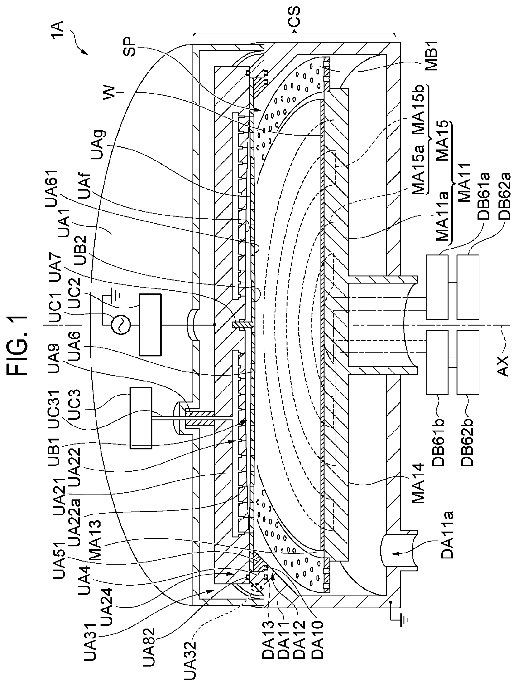
The configuration of a plasma processing apparatus 1 A illustrated in will be described. The plasma processing apparatus 1 A includes a process container CS. The plasma processing apparatus 1 A includes a space SP, a waveguide wall UA 1 , an upper electrode UA 21 , a cavity UA 22 , and a waveguide UA 31 . The plasma processing apparatus 1 A includes an insulating member UA 4 , a support ring UA 51 , a dielectric plate UA 6 , a dielectric rod UA 7 , a sealing member UA 82 , a tube UA 9 , an gap UB 1 , and a gas pipe UC 31 .
The plasma processing apparatus 1 A includes a side wall DA 11 , an exhaust port DA 11 a , a sealing member DA 13 , a common mode filter DB 61 a , a common mode filter DB 61 b , a heater power supply DB 62 a , and a heater power supply DB 62 b.
The plasma processing apparatus 1 A includes a stage MA 11 and a baffle member MB 1 .
The process container CS has substantially a cylindrical shape. The process container CS extends along the vertical direction.
A central axial line of the process container CS is an axial line AX extending in the vertical direction. The process container CS includes the waveguide wall UA 1 , the side wall DA 11 , and the waveguide UA 31 .
In the present disclosure, a direction in which the axial line AX extends is referred to as a reference direction. In other words, the reference direction is a direction intersecting the lower surface UAf of the upper electrode UA 21 exposed to the gap UB 1 .
A ceiling portion of the waveguide wall UA 1 extends (substantially horizontally) to a plane intersecting the axial line AX. A side portion of the waveguide wall UA 1 extends perpendicularly to the ceiling portion of the waveguide wall UA 1 along the axial line AX. The waveguide wall UA 1 surrounds the upper electrode UA 21 of the plasma processing apparatus 1 A.
The material of the waveguide wall UA 1 can be a conductive material such as aluminum or an aluminum alloy. The waveguide wall UA 1 is grounded.
The waveguide UA 31 is defined by a space between the waveguide wall UA 1 and the upper electrode UA 21 . The waveguide UA 31 guides a high frequency of a VHF band or an UHF band and introduces the high frequency into the space SP. In the present disclosure, the high frequency means a high frequency of a VHF band or an UHF band.
The waveguide UA 31 includes an end portion UA 32 from which a high frequency is radiated. The end portion UA 32 is located toward the space SP.
The end portion UA 32 radiates the high frequency into the space SP via the insulating member UA 4 and the insulating support ring UA 51 . The space SP is a space between the dielectric plate UA 6 and the stage MA 11 .
The side wall DA 11 extends along the axial line AX below the side portion of the waveguide wall UA 1 . The side wall DA 11 extends along the axial line AX below the waveguide wall UA 1 .
The material of the side wall DA 11 can be a conductive material such as aluminum or an aluminum alloy. The side wall DA 11 is grounded.
The side wall DA 11 includes a projection DA 12 . The projection DA 12 of the side wall DA 11 is provided at an end portion of the side wall DA 11 (a portion connected to the side portion of the waveguide wall UA 1 ) and extends toward the axial line AX in a direction intersecting the axial line AX. The projection DA 12 is connected to the insulating member UA 4 via the sealing member DA 13 . The sealing member DA 13 is a member for vacuum sealing and may be, for example, an O-ring.
The projection DA 12 is connected to the support ring UA 51 via an elastic member DA 10 . The support ring UA 51 is provided on the projection DA 12 . The elastic member DA 10 is provided for pressing.
The insulating member UA 4 is interposed between the end portion UA 32 , the support ring UA 51 , and the space SP. The insulating member UA 4 and the upper electrode UA 21 are connected via the sealing member UA 82 . The material of the insulating member UA 4 may be an insulating material such as aluminum nitride or aluminum oxide. The sealing member UA 82 is a member for vacuum sealing and may be, for example, an O-ring.
The upper electrode UA 21 is provided above the dielectric plate UA 6 . The upper electrode UA 21 is accommodated in the waveguide wall UA 1 . The upper electrode UA 21 is disposed below the ceiling portion of the waveguide wall UA 1 and is surrounded by the side portion of the waveguide wall UA 1 .
The upper electrode UA 21 is provided above the upper surface MA 13 of the stage MA 11 via the space SP and the dielectric plate UA 6 in the process container CS. The upper electrode UA 21 is electrically connected to a high frequency power supply UC 1 via a matching device UC 2 .
The material of the upper electrode UA 21 can be a conductive material such as aluminum or an aluminum alloy. A corrosion-resistant film is formed on the surface of the upper electrode UA 21 . The corrosion-resistant film may be an aluminum oxide film, an yttrium oxide film, or a ceramic film containing aluminum oxide, yttrium oxide, or the like.
The high frequency power supply UC 1 is a power supply that generates the above-mentioned high frequency. The matching device UC 2 includes a matching circuit that matches the load impedance of the high frequency power supply UC 1 with the output impedance of the high frequency power supply UC 1 .
The upper electrode UA 21 includes the cavity UA 22 . The upper electrode UA 21 has a plurality of gas discharge holes UA 22 a (first gas discharge holes). The cavity UA 22 communicates with a gas supply part UC 3 via the gas pipe UC 31 .
The cavity UA 22 communicates with the plurality of gas discharge holes UA 22 a . The cavity UA 22 communicates with the space SP via the plurality of gas discharge holes UA 22 a and further the gap UB 1 and a plurality of gas discharge holes UB 2 of the dielectric plate UA 6 .
The dielectric plate UA 6 is provided directly below the upper electrode UA 21 . The dielectric plate UA 6 is provided above the upper surface MA 13 of the stage MA 11 via the space SP in the process container CS.
The dielectric plate UA 6 has the plurality of gas discharge holes UB 2 (second gas discharge holes). In one embodiment, the dielectric plate UA 6 is a shower plate.
The plurality of gas discharge holes UA 22 a and the plurality of gas discharge holes UB 2 communicate with each other via the gap UB 1 . At least some of the plurality of gas discharge holes UA 22 a and at least some of the plurality of gas discharge holes UB 2 are provided so as to overlap each other when viewed from above the upper electrode UA 21 (the direction of the axial line AX). For example, it is configured that the gas discharge holes UA 22 a and the gas discharge holes UB 2 arranged in portions where the width of the gap UB 1 is smaller more overlap each other.
An end portion of the dielectric plate UA 6 is brought into close contact with an end portion of the upper electrode UA 21 by the support ring UA 51 . The dielectric plate UA 6 faces the upper surface MA 13 of the stage MA 11 via the space SP.
A central axial line of the dielectric plate UA 6 substantially coincides with the axial line AX. The plurality of gas discharge holes UB 2 are arranged on the dielectric plate UA 6 so that a gas is evenly supplied to the entire surface of a substrate W (object to be processed) placed on the upper surface MA 13 of the stage MA 11 .
A distance (the width of the space SP) in the vertical direction between the lower surface of the dielectric plate UA 6 and the upper surface MA 13 of the stage MA 11 can be, for example, 5 [cm] or more and 30 [cm] or less.
The dielectric plate UA 6 has a flat plate shape and is flexible. The material of the dielectric plate UA 6 can be a dielectric such as aluminum nitride or aluminum oxide. The thickness of the dielectric plate UA 6 can be substantially uniform. The dielectric plate UA 6 has substantially a disc shape. The dielectric plate UA 6 is formed of aluminum nitride, aluminum oxide, yttrium oxide, or a dielectric containing aluminum nitride, aluminum oxide, yttrium oxide, or the like. A corrosion-resistant film may be formed on the surface (particularly, the lower surface UA 61 ) of the dielectric plate UA 6 . The corrosion-resistant film may be an yttrium oxide film, an yttrium oxyfluoride film, an yttrium fluoride film, or a ceramic film containing yttrium oxide, yttrium fluoride, or the like.
The support ring UA 51 is a member that closely adheres the dielectric plate UA 6 to the upper electrode UA 21 . The support ring UA 51 is connected to the insulating member UA 4 . The material of the support ring UA 51 can be an insulating material such as aluminum nitride or aluminum oxide.
The insulating member UA 4 and the support ring UA 51 are juxtaposed on the projection DA 12 of the side wall DA 11 . The insulating member UA 4 and the support ring UA 51 are sandwiched between the projection DA 12 and an outer peripheral portion UA 24 of the upper electrode UA 21 .
The dielectric rod UA 7 is interposed between the upper electrode UA 21 and the dielectric plate UA 6 . The dielectric rod UA 7 can be disposed on the axial line AX. The dielectric rod UA 7 extends along the axial line AX.
The dielectric rod UA 7 is connected to the upper electrode UA 21 . The dielectric rod UA 7 is in contact with the dielectric plate UA 6 or is joined (fixed) to the dielectric plate UA 6 . The material of the dielectric rod UA 7 can be a dielectric such as aluminum nitride or aluminum oxide.
The gap UB 1 may be provided between the upper electrode UA 21 and the dielectric plate UA 6 . The gap UB 1 can be formed by separating the upper electrode UA 21 and the dielectric plate UA 6 from each other. The gap UB 1 is defined by the lower surface UAf of the upper electrode UA 21 and an upper surface UAg of the dielectric plate UA 6 . The lower surface UAf of the upper electrode UA 21 may be an upwardly convex curved surface. The width of the gap UB 1 follows a function of the radial position (generally a cosine function or a Gaussian function).
The gap UB 1 is defined by separating the upper electrode UA 21 and the dielectric plate UA 6 from each other in a state where the end portion (the outer peripheral portion UA 24 ) of the upper electrode UA 21 and the end portion of the dielectric plate UA 6 are in close contact with each other.
The upper electrode UA 21 and the dielectric plate UA 6 are farthest from each other on the axial line AX on which the dielectric rod UA 7 is disposed. The width of the gap UB 1 (a distance between the lower surface UAf of the upper electrode UA 21 and the upper surface UAg of the dielectric plate UA 6 ) is not uniform (constant), that is, non-uniform, in a direction in which the dielectric plate UA 6 (and a dielectric plate UA 6 a to be described later) extends. When the gap UB 1 is provided between the upper electrode UA 21 and plasma in this way, a high frequency current flowing from the plasma is reduced, suppressing excitation of the plasma. By optimizing the width of the gap UB 1 in the plane of the upper electrode UA 21 as in the present embodiment, uniform plasma can be generated on the upper portion of the substrate W.
The stage MA 11 includes a main body MA 11 a and a conductive layer MA 15 . The stage MA 11 is provided in the process container CS. The stage MA 11 is configured to substantially horizontally support the substrate W placed on the upper surface MA 13 of the stage MA 11 .
The stage MA 11 has substantially a disc shape. The central axial line of the stage MA 11 substantially coincides with the axial line AX.
The conductive layer MA 15 functions as a heater (resistive heating element) that heats the substrate W placed on the upper surface MA 13 through the upper surface MA 13 of the stage MA 11 . The conductive layer MA 15 includes a heater member MA 15 a and a heater member MA 15 b . The material of the conductive layer MA 15 can be metal such as tungsten or molybdenum.
The heater member MA 15 a and the heater member MA 15 b are buried inside the main body MA 11 a . The heater member MA 15 a and the heater member MA 15 b are not in contact with each other. The material of the main body MA 11 a is an insulator such as aluminum nitride or aluminum oxide.
A heating region of the stage MA 11 is divided into two zones in the radial direction. Each of the zones is heated by the conductive layer MA 15 .
The heater member MA 15 a heats a zone in the center portion of the main body MA 11 a . The heater member MA 15 b heats a zone in the outer peripheral portion of the main body MA 11 a.
The common mode filter DB 61 a is electrically connected to the heater member MA 15 a . The heater power supply DB 62 b is electrically connected to the common mode filter DB 61 a.
The common mode filter DB 61 b is electrically connected to the heater member MA 15 b . The heater power supply DB 62 b is electrically connected to the common mode filter DB 61 b . The common mode filter DB 61 a is provided between the heater member MA 15 a and the heater power supply DB 62 a , and the common mode filter DB 61 b is provided between the heater member MA 15 b and the heater power supply DB 62 b.
The common mode filter DB 61 a and the common mode filter DB 61 b each has a relatively high common mode impedance at a plasma excitation frequency. Therefore, the electrical coupling between the heater member MA 15 a and the heater member MA 15 b can be weakened. As a result, at the outer peripheral portion and the center portion of the main body MA 11 a of the stage MA 11 , the electrical coupling between plasma, the heater member MA 15 a , and the heater member MA 15 b is suppressed, so that a high frequency electric field applied between the center portion and the end portion of the substrate W can be suppressed.
The baffle member MB 1 extends between the stage MA 11 and the side wall DA 11 . The baffle member MB 1 is substantially an annular plate material. The material of the baffle member 13 can be, for example, an insulator such as aluminum nitride or aluminum oxide.
A plurality of through-holes are formed in the baffle member MB 1 . The plurality of through-holes penetrate the baffle member MB 1 in its thickness direction of the plate.
A region under the back surface MA 14 of the stage MA 11 communicates with the exhaust port DA 11 a . The exhaust port DA 11 a is connected to an external exhaust device. The exhaust device may include a pressure control valve and a vacuum pump such as a turbo molecular pump and/or a dry pump.
The gas supply part UC 3 is connected to the plasma processing apparatus 1 A. The gas supply part UC 3 is protected from a high frequency by the insulating tube UA 9 and is connected to the gas pipe UC 31 communicating with the cavity UA 22 in the upper electrode UA 21 .
A gas from the gas supply part UC 3 is supplied into the space SP via the gas pipe UC 31 , the cavity UA 22 , the plurality of gas discharge holes UA 22 a , the gap UB 1 , and the plurality of gas discharge holes UB 2 sequentially. The gas supply part UC 3 includes one or more gas sources used for processing the substrate W. The gas supply part UC 3 includes one or more flow rate controllers for controlling the flow rate of gases from the one or more gas sources.
The gas pipe UC 31 that communicates the gas supply part UC 3 and the cavity UA 22 with each other is covered with the insulating tube UA 9 in the waveguide UA 31 and is protected from a high frequency in the waveguide UA 31 by the tube UA 9 . The material of the tube UA 9 can be an insulating material such as aluminum nitride or aluminum oxide.
In the plasma processing apparatus 1 A, the area of the inner wall surface (more specifically, the side wall DA 11 ) of the process container CS extending from the upper side of the baffle member MB 1 is approximately equal to the surface area of the dielectric plate UA 6 (the area of the lower surface UA 61 ) on the space SP side. That is, the area of a plane set to the ground potential (ground plane) among planes defining the space SP is approximately equal to the area of a plane provided by the dielectric plate UA 6 among the planes defining the space SP. With this configuration, plasma is generated at a uniform density in a region directly below the dielectric plate UA 6 and a region around the ground plane. This results in improvement of the in-plane uniformity of the plasma processing of the substrate W.
In the plasma processing apparatus 1 A, a high frequency is introduced from the end portion UA 32 of the waveguide UA 31 into the space SP toward the axial line AX. When the high frequency is introduced into the space SP, a gas is excited in the space SP and plasma is generated from the gas. The plasma is generated in the space SP with a uniform density distribution in the circumferential direction. The substrate W on the stage MA 11 is processed with chemical species from the plasma.
Hereinafter, a plasma processing apparatus 1 B according to another exemplary embodiment will be described with reference to . A distance (the width of a space SP) in the vertical direction between the lower surface UA 61 of a dielectric plate UA 6 and the upper surface MA 13 of a stage MA 11 in the plasma processing apparatus 1 B can be shorter than that in the case of the plasma processing apparatus 1 A. This distance may be, for example, 5 [mm] or more and 15 [mm] or less. The configuration of the plasma processing apparatus 1 B is different from the configuration of the plasma processing apparatus 1 A depending on the difference in the width of the space SP.
The plasma processing apparatus 1 B includes a process container CS. The plasma processing apparatus 1 B includes a space SP, a waveguide wall UA 1 , an upper electrode UA 21 , a cavity UA 22 , a waveguide UA 31 , an insulating member UA 4 , a support ring UA 51 , a cover ring UA 52 , a dielectric plate UA 6 , an elastic member UA 81 , a sealing member UA 82 , and a tube UA 9 . The plasma processing apparatus 1 B includes an gap UB 1 , a gas pipe UC 31 , and a drive mechanism UD 10 .
The plasma processing apparatus 1 B includes a stage MA 11 , a conductive part MA 21 , a conductive plate MA 22 , a conductive elastic member MA 23 , an exhaust chamber MA 31 , a wall part MA 32 , and a vent hole MA 33 .
The plasma processing apparatus 1 B includes a sealing member DA 13 , an inlet/outlet DA 2 , a support part DB 11 , an exhaust pipe DB 12 , a bellows DB 21 , a bellows DB 22 , a spring DB 3 , and a water cooling plate DB 4 .
The process container CS includes the waveguide wall UA 1 , a side wall DA 11 , and the waveguide UA 31 .
Hereinafter, the description of the plasma processing apparatus 1 B will be given mainly to only a configuration different from that of the plasma processing apparatus 1 A.
A projection DA 12 of the side wall DA 11 is provided at an end portion of the side wall DA 11 (a portion connected to a side portion of the waveguide wall UA 1 ) and extends in a direction intersecting an axial line AX toward the axial line AX.
The projection DA 12 is connected to the wall part MA 32 of the exhaust chamber MA 31 via the conductive elastic member MA 23 . The conductive elastic member MA 23 is an elastic body and may be, for example, a spiral ring. The material of the conductive elastic member MA 23 is, for example, metal such as stainless steel, Inconel, nickel, tungsten, tantalum, a copper alloy, or molybdenum. The conductive elastic member MA 23 may be coated with a protective film such as nickel, aluminum, stainless steel or gold.
The insulating member UA 4 is interposed between the end portion UA 32 of the waveguide UA 31 and the space SP.
The support ring UA 51 is connected to the insulating member UA 4 via the elastic member UA 81 . The elastic member UA 81 can be, for example, a stainless steel spring.
The end portion of the dielectric plate UA 6 and the end portion (the outer peripheral portion UA 24 ) of the upper electrode UA 21 are connected to each other by pressing via the elastic member UA 81 or the like.
The cover ring UA 52 is a member that prevents plasma from being generated in the vicinity of the side surface of the stage MA 11 . The material of the cover ring UA 52 can be an insulating material such as aluminum nitride or aluminum oxide.
The plasma processing apparatus 1 B further includes the drive mechanism UD 10 . The drive mechanism UD 10 includes a motor UD 11 , an insulating shaft UD 12 , a pulley UD 13 (first pulley), a belt UD 14 , and a driving part UD 15 a.
The motor UD 11 is provided on the waveguide wall UA 1 . The pulley UD 13 , the belt UD 14 , and the driving part UD 15 a (further, a driving part UD 15 b illustrated in to be described later) are provided in the upper electrode UA 21 .
The insulating shaft UD 12 is connected to the motor UD 11 . The pulley UD 13 connects the insulating shaft UD 12 and the belt UD 14 .
The insulating shaft UD 12 rotates by the rotational drive of the motor UD 11 . The pulley UD 13 changes the rotational movement of the insulating shaft UD 12 into the linear movement of the belt UD 14 .
The linear movement of the belt UD 14 is transmitted to the driving part UD 15 a , so that the movement of a dielectric rod UD 15 a 9 (which will be described later with reference to ) of the driving part UD 15 a (the movement in the reference direction intersecting the lower surface UAf of the upper electrode UA 21 ) can be performed. The configuration of the driving part UD 15 a will be described in detail later.
The gap UB 1 is formed by separating the upper electrode UA 21 and the dielectric plate UA 6 from each other. The width of the gap UB 1 (a distance between the upper electrode UA 21 and the dielectric plate UA 6 ) can be adjusted by the drive mechanism UD 10 . The upper electrode UA 21 and the dielectric plate UA 6 can be farthest from each other on the axial line AX on which the driving part UD 15 a having the dielectric rod UD 15 a 9 is disposed.
The material of the stage MA 11 of the plasma processing apparatus 1 B can be a conductive material such as aluminum or an aluminum alloy. A protective film made of yttrium oxide, yttrium oxyfluoride, or aluminum oxide may be provided on the surface of the stage MA 11 .
The exhaust chamber MA 31 includes the conductive wall part MA 32 . The exhaust chamber MA 31 extends from around the outer peripheral portion MA 12 toward the side wall DA 11 .
The wall part MA 32 includes the vent hole MA 33 . The exhaust chamber MA 31 communicates with the space SP. The space SP communicates with the exhaust chamber MA 31 via the vent hole MA 33 . The exhaust chamber MA 31 communicates with the exhaust pipe DB 12 .
The material of the wall part MA 32 can be a conductive material such as aluminum or an aluminum alloy.
The exhaust pipe DB 12 is connected to an external exhaust device. The exhaust device system may include a pressure control valve and a vacuum pump such as a turbo molecular pump and/or a dry pump.
A gas in the space SP can move to the exhaust chamber MA 31 through the vent hole MA 33 and can be exhausted to the outside through the exhaust pipe DB 12 .
The conductive part MA 21 extends between the outer peripheral portion MA 12 of the stage MA 11 and the side wall DA 11 of the process container CS. The conductive part MA 21 is electrically connected to a conductive layer of the stage MA 11 and the side wall DA 11 of the process container CS.
The conductive part MA 21 extends from the outer peripheral portion MA 12 toward the side wall DA 11 so that a high frequency radiated from the end portion UA 32 of the waveguide UA 31 is introduced into the space SP. The conductive part MA 21 includes the conductive plate MA 22 . The conductive part MA 21 includes a portion of the wall part MA 32 .
The conductive plate MA 22 is in electrical contact with the back surface MA 14 of the stage MA 11 at the outer peripheral portion MA 12 . The conductive plate MA 22 is joined (fixed) to the back surface of the outer peripheral portion MA 12 and the upper surface of the wall part MA 32 by screws (not shown).
The conductive plate MA 22 is a flexible thin plate. The material of the conductive plate MA 22 is, for example, a conductive material such as aluminum, an aluminum alloy, stainless steel, Inconel, nickel, tungsten, tantalum, a copper alloy, or molybdenum. The conductive plate MA 22 may be coated with a protective film such as aluminum oxide, yttrium oxide, yttrium oxyfluoride, yttrium fluoride, nickel, aluminum, stainless steel, or gold.
The side wall DA 11 includes the inlet/outlet DA 2 . A substrate W is loaded into and unloaded from the process container CS via the inlet/outlet DA 2 .
The support part DB 11 is connected to the stage MA 11 . The stage MA 11 is provided on the support part DB 11 . The stage MA 11 moves up and down by moving the support part DB 11 up and down (by approaching the upper electrode UA 21 or moving away from the upper electrode UA 21 , the same applies hereinafter).
A water-cooled plate DB 4 is disposed below the support part DB 11 . The support part DB 11 is in contact with the water-cooled plate DB 4 . The heat of the stage MA 11 can be discharged to the outside through the support part DB 11 and the water-cooled plate DB 4 .
The exhaust pipe DB 12 is connected to the wall part MA 32 and communicates with the exhaust chamber MA 31 . The wall part MA 32 is provided on the exhaust pipe DB 12 . A gas in the exhaust chamber MA 31 can be discharged to the outside through the exhaust pipe DB 12 .
The exhaust chamber MA 31 and the wall part MA 32 move up and down by moving the exhaust pipe DB 12 up and down through the spring DB 3 .
The material of the bellows DB 22 can be a conductive material such as stainless steel. The material of the spring DB 3 can be a conductive material such as stainless steel.
The wall part MA 32 can be stably disposed on the side (upper side) of the upper electrode UA 21 due to the elasticity of the spring DB 3 . As a result, the outer peripheral portion of the wall part MA 32 comes into close contact with the back surface of the projection DA 12 . Further, the outer peripheral portion of the wall part MA 32 can come in stable and electrical contact with the projection DA 12 due to the elasticity of the conductive elastic member MA 23 .
In the plasma processing apparatus 1 B, a high frequency is introduced into the space SP from the end portion UA 32 of the waveguide UA 31 via the insulating member UA 4 toward the axial line AX. When the high frequency is introduced into the space SP, a gas is excited in the space SP and plasma is generated from the gas. The plasma is generated in the space SP with a uniform density distribution in the circumferential direction. The substrate W on stage MA 11 is processed with chemical species from the plasma. Further, discharge to the peripheral portion of the space SP can be suppressed by the insulating member UA 4 .
Hereinafter, the configuration of the driving part UD 15 a will be described with reference to . The driving part UD 15 a includes a pulley UD 15 a 1 (second pulley), an adjusting screw UD 15 a 2 , a container UD 15 a 3 , a shaft UD 15 a 4 , and a spring UD 15 a 5 . The material of the spring UD 15 a 5 can be, for example, stainless steel.
The driving part UD 15 a further includes an O-ring UD 15 a 6 , a male portion UD 15 a 8 of a floating joint, and a dielectric rod UD 15 a 9 . The material of the dielectric rod UD 15 a 9 can be a dielectric such as aluminum nitride or aluminum oxide.
The dielectric rod UD 15 a 9 is interposed between the upper electrode UA 21 and the dielectric plate UA 6 . The dielectric rod UD 15 a 9 can be disposed on the axial line AX.
The dielectric rod UD 15 a 9 is integrated with the dielectric plate UA 6 or is connected or joined (fixed) to the dielectric plate UA 6 .
In a state where the end portion of the dielectric plate UA 6 is brought into close contact with the end portion (the outer peripheral portion UA 24 ) of the upper electrode UA 21 by the support ring UA 51 , the dielectric rod UD 15 a 9 can increase or decrease a distance (the width of the gap UB 1 ) between the upper electrode UA 21 and the dielectric plate UA 6 .
The drive mechanism UD 10 including the driving part UD 15 a drives the dielectric rod UD 15 a 9 in the reference direction to increase or decrease the width of the gap UB 1 . The driving part UD 15 a connects the dielectric rod UD 15 a 9 and the belt UD 14 and drives the dielectric rod UD 15 a 9 in the reference direction by using the power of the motor UD 11 transmitted via the insulating shaft UD 12 and the belt UD 14 .
The pulley UD 15 a 1 includes the adjusting screw UD 15 a 2 . The pulley UD 15 a 1 connects the belt UD 14 and the shaft UD 15 a 4 . The shaft UD 15 a 4 includes a female portion UD 15 a 7 of the floating joint.
The central axes of the adjusting screw UD 15 a 2 and the shaft UD 15 a 4 substantially coincide with the axial line AX. Each of the adjusting screw UD 15 a 2 and the shaft UD 15 a 4 can move linearly along the axial line AX.
The shaft UD 15 a 4 is connected to the dielectric rod UD 15 a 9 via the floating joint (the female portion UD 15 a 7 of the floating joint and the male portion UD 15 a 8 of the floating joint).
The central axes of the female portion UD 15 a 7 of the floating joint, the male portion UD 15 a 8 of the floating joint, and the dielectric rod UD 15 a 9 substantially coincide with the axial line AX. Each of the female portion UD 15 a 7 of the floating joint, the male portion UD 15 a 8 of the floating joint, and the dielectric rod UD 15 a 9 can move linearly along the axial line AX.
The pulley UD 15 a 1 is connected to the belt UD 14 . The pulley UD 15 a 1 changes the linear movement of the belt UD 14 into the rotational movement of the adjusting screw UD 15 a 2 around the axial line AX and the linear movement of the adjusting screw UD 15 a 2 along the axial line AX.
The adjusting screw UD 15 a 2 is held in the container UD 15 a 3 . The container UD 15 a 3 is joined (fixed) in the upper electrode UA 21 . The upper end of the shaft UD 15 a 4 and the spring UD 15 a 5 are accommodated in the container UD 15 a 3 .
The lower end of the adjusting screw UD 15 a 2 contacts the upper end of the shaft UD 15 a 4 . The lower end of the adjusting screw UD 15 a 2 is brought into close contact with the upper end of the shaft UD 15 a 4 by the elastic force of the spring UD 15 a 5 . The shaft UD 15 a 4 moves linearly along the axial line AX in accordance with the linear movement of the adjusting screw UD 15 a 2 along the axial line AX.
The O-ring UD 15 a 6 can stabilize the disposition of the shaft UD 15 a 4 in the upper electrode UA 21 and seal the gap UB 1 .
The lower end of the shaft UD 15 a 4 has the female portion UD 15 a 7 of the floating joint. The male portion UD 15 a 8 of the floating joint is fitted into the female portion UD 15 a 7 of the floating joint. The male portion UD 15 a 8 of the floating joint moves linearly along the axial line AX in accordance with the linear movement of the shaft UD 15 a 4 along the axial line AX.
The lower end of the male portion UD 15 a 8 of the floating joint is connected to the dielectric rod UD 15 a 9 . The dielectric rod UD 15 a 9 moves linearly along the axial line AX in accordance with the linear movement of the male portion UD 15 a 8 of the floating joint along the axial line AX.
That is, the dielectric rod UD 15 a 9 can move linearly along the axial line AX due to the rotational movement of the insulating shaft UD 12 by the motor UD 11 . More specifically, the dielectric rod UD 15 a 9 can receive power from the motor UD 11 via the floating joint. Therefore, even if the axes of the shaft UD 15 a 4 and the dielectric rod UD 15 a 9 are slightly deviated from each other, the dielectric plate UA 6 and the upper electrode UA 21 can be separated from and brought close to each other by driving the dielectric rod UD 15 a 9 .
Further, since the rotational movement of the insulating shaft UD 12 by the motor UD 11 can be transmitted to the adjusting screw UD 15 a 2 by the belt UD 14 , the motor UD 11 can be provided at a position away from the axial line AX on the ceiling portion of the waveguide wall UA 1 . Therefore, the disposition position of the motor UD 11 can be selected relatively flexibly on the waveguide wall UA 1 .
The drive mechanism UD 10 can include the driving part UD 15 b illustrated in in place of the above-described driving part UD 15 a . The driving part UD 15 b is disposed in the upper electrode UA 21 in the same manner as the driving part UD 15 a.
The driving part UD 15 b includes a pulley UD 15 b 1 (second pulley), an adjusting screw UD 15 b 2 , a container UD 15 b 3 , a ball UD 15 b 4 , a shaft UD 15 b 5 , a bellows UD 15 b 6 , and a dielectric rod UD 15 b 7 .
The dielectric rod UD 15 b 7 is interposed between the upper electrode UA 21 and the dielectric plate UA 6 . The dielectric rod UD 15 b 7 can be disposed on the axial line AX.
The lower portion of the dielectric rod UD 15 b 7 is fitted into a hole provided in the upper surface UAg of the dielectric plate UA 6 . The material of the dielectric rod UD 15 b 7 can be a dielectric such as aluminum nitride or aluminum oxide.
The drive mechanism UD 10 including the driving part UD 15 b can linearly move the dielectric rod UD 15 b 7 along the reference direction so as to separate the upper electrode UA 21 from the dielectric plate UA 6 , so that the width of the gap UB 1 can be increased.
The driving part UD 15 b connects the dielectric rod UD 15 b 7 and the belt UD 14 and drives the dielectric rod UD 15 b 7 in the reference direction by using the power of the motor UD 11 transmitted via the insulating shaft UD 12 and the belt UD 14 .
The pulley UD 15 b 1 includes the adjusting screw UD 15 b 2 . The pulley UD 15 b 1 connects the belt UD 14 to the shaft UD 15 b 5 . The shaft UD 15 b 5 is connected to the dielectric rod UD 15 b 7 .
The central axes of the adjusting screw UD 15 b 2 , the shaft UD 15 b 5 , and the dielectric rod UD 15 b 7 substantially coincide with the axial line AX. Each of the adjusting screw UD 15 b 2 , the shaft UD 15 b 5 , and the dielectric rod UD 15 b 7 can move linearly along the axial line AX.
The pulley UD 15 b 1 is connected to the belt UD 14 . The pulley UD changes the linear movement of the belt UD 14 into the rotational movement of the adjusting screw UD 15 b 2 around the axial line AX and the linear movement of the adjusting screw UD 15 b 2 along the axial line AX.
The adjusting screw UD 15 b 2 is held in the container UD 15 b 3 . The container UD 15 b 3 is connected to the upper electrode UA 21 . The ball UD 15 b 4 , the upper end of the shaft UD 15 b 5 , and the bellows UD 15 b 6 are accommodated in the container UD 15 a 3 .
The lower end of the adjusting screw UD 15 b 2 is connected to the upper end of the shaft UD 15 b 5 via the ball UD 15 b 4 . The upper end of the shaft UD 15 b 5 is brought into close contact with the lower end of the adjusting screw UD 15 b 2 via the ball UD 15 b 4 by the elastic force of the bellows UD 15 b 6 . The lower end of the adjusting screw UD 15 b 2 is brought into close contact with the ball UD 15 b 4 in a state where the ball UD 15 b 4 is pressed by the adjusting screw UD 15 b 2 . The shaft UD 15 b 5 moves linearly along the axial line AX in accordance with the linear movement of the adjusting screw UD 15 b 2 along the axial line AX.
In this way, since the adjusting screw UD 15 b 2 and the shaft UD 15 b 5 are not joined (fixed) (connected via the ball UD 15 b 4 ), they can be separated from each other.
The bellows UD 15 b 6 can seal the gap UB 1 . The material of the bellows UD 15 b 6 can be stainless steel, an aluminum alloy, or the like.
The lower end of the shaft UD 15 b 5 is connected to the upper end of the dielectric rod UD 15 b 7 . The lower end of the dielectric rod UD 15 b 7 is connected to the dielectric plate UA 6 . The dielectric rod UD 15 b 7 moves linearly along the axial line AX in accordance with the linear movement of the shaft UD 15 b 5 along the axial line AX.
That is, the dielectric rod UD 15 b 7 can move linearly along the axial line AX due to the rotational movement of the insulating shaft UD 12 by the motor UD 11 . More specifically, the dielectric rod UD 15 b 7 can be driven to separate the dielectric plate UA 6 from the upper electrode UA 21 .
Further, since the rotational movement of the insulating shaft UD 12 by the motor UD 11 can be transmitted to the adjusting screw UD 15 b 2 by the belt UD 14 , the motor UD 11 can be provided at a position away from the axial line AX on the ceiling portion of the waveguide wall UA 1 . Therefore, the disposition position of the motor UD 11 can be selected relatively flexibly on the waveguide wall UA 1 .
Hereinafter, a plasma processing apparatus 1 C according to another exemplary embodiment will be described with reference to . The plasma processing apparatus 1 C includes a process container CS. The plasma processing apparatus 1 C includes a space SP, a waveguide wall UA 1 , an upper electrode UA 21 a , a waveguide UA 31 , an insulating member UA 4 , a dielectric plate UA 6 a , a sealing member UA 82 , a sealing member UA 83 , a tube UA 9 , an gap UB 1 , and a gas pipe UC 31 .
The plasma processing apparatus 1 C includes a side wall DA 11 , an exhaust port DA 11 a , a sealing member DA 13 , and an elastic member DA 14 .
The plasma processing apparatus 1 C includes a stage MA 11 and a plasma shielding plate MB 2 .
The process container CS includes the waveguide wall UA 1 , the side wall DA 11 , and the waveguide UA 31 .
Hereinafter, the description of the plasma processing apparatus 1 C will be given mainly to only a configuration different from those of the plasma processing apparatus 1 A and the plasma processing apparatus 1 B.
The side wall DA 11 includes a gas chamber MA 41 , a wall part MA 42 , and a plurality of gas discharge grooves MA 43 .
The gas chamber MA 41 , the wall part MA 42 , and the gas discharge grooves MA 43 are provided at the end portion of the side wall DA 11 (a portion connected to the side portion of the waveguide wall UA 1 ) and extend to a direction intersecting the axis line AX toward the axis line AX. The wall part MA 42 is connected to the insulating member UA 4 via the sealing member DA 13 .
A gas supplier UD 2 is connected to the gas chamber MA 41 , and a gas supplied from the gas supplier UD 2 can be stored in the gas chamber MA 41 . The gas discharge grooves MA 43 are connected to the gas chamber MA 41 , and the gas stored in the gas chamber MA 41 is supplied to the upper side of the space SP (directly below the lower surface UA 61 of the dielectric plate UA 6 a ) via the gas discharge grooves MA 43 .
The upper electrode UA 21 a is provided above the dielectric plate UA 6 a . The upper electrode UA 21 a is accommodated in the waveguide wall UA 1 . The upper electrode UA 21 a is disposed below the ceiling portion of the waveguide wall UA 1 and is surrounded by the side portion of the waveguide wall UA 1 .
The upper electrode UA 21 a is provided above the upper surface MA 13 of the stage MA 11 via the space SP and the dielectric plate UA 6 a in the process container CS. The upper electrode UA 21 a is electrically connected to a high frequency power supply UC 1 via a matching device UC 2 .
The material of the upper electrode UA 21 a can be a conductive material such as aluminum or an aluminum alloy. A corrosion-resistant film is formed on the surface of the upper electrode UA 21 a . The corrosion-resistant film can be an aluminum oxide film, an yttrium oxide film, or a ceramic film containing aluminum oxide, yttrium oxide, or the like.
The dielectric plate UA 6 a is a dielectric cover and is provided directly below the upper electrode UA 21 a in the space SP. The dielectric plate UA 6 a is provided above the upper surface MA 13 of the stage MA 11 via the space SP in the process container CS.
The end portion of the dielectric plate UA 6 a is brought into close contact with the end portion (the outer peripheral portion UA 24 ) of the upper electrode UA 21 a by the insulating member UA 4 . The end of the dielectric plate UA 6 a is connected to the upper electrode UA 21 a via the elastic member DA 14 and to the insulating member UA 4 via the sealing member UA 83 . The sealing member UA 83 is a member for vacuum sealing and can be, for example, an O-ring. The sealing member UA 83 can prevent a gas above the dielectric plate UA 6 a from leaking into the space SP.
The elastic member DA 14 can be an O-ring or the like. The dielectric plate UA 6 a faces the upper surface MA 13 of the stage MA 11 via the space SP. The central axial line of the dielectric plate UA 6 a substantially coincides with the axial line AX.
The dielectric plate UA 6 a has flexibility. The dielectric plate UA 6 a is formed of aluminum nitride, aluminum oxide, yttrium oxide, or a dielectric containing aluminum nitride, aluminum oxide, yttrium oxide, or the like. A corrosion-resistant film may be formed on the surface (particularly, the lower surface UA 61 ) of the dielectric plate UA 6 a . The corrosion-resistant film can be an yttrium oxide film, an yttrium oxyfluoride film, an yttrium fluoride film, or a ceramic film containing yttrium oxide, yttrium fluoride, or the like. The thickness of the dielectric plate UA 6 a can be substantially uniform.
The dielectric plate UA 6 a has substantially a disc shape. A distance (the width of the space SP) in the vertical direction between the lower surface of the dielectric plate UA 6 a and the upper surface MA 13 of the stage MA 11 can be, for example, 5 [cm] or more and 10 [cm] or less. The insulating member UA 4 brings the dielectric plate UA 6 a into close contact with the upper electrode UA 21 a.
The gap UB 1 is formed by separating the upper electrode UA 21 a and the dielectric plate UA 6 a from each other. More specifically, the gap UB 1 is a space between the lower surface UAf of the upper electrode UA 21 a and the upper surface UAg of the dielectric plate UA 6 a and is defined by the lower surface UAf and the upper surface UAg. The upper electrode UA 21 a and the dielectric plate UA 6 a can be farthest from each other on the axial line AX in a state where the end portion of the dielectric plate UA 6 a is brought into close contact with the end portion (the outer peripheral portion UA 24 ) of the upper electrode UA 21 a by the insulating member UA 4 .
The gas pipe UC 31 connected to an external gas supply part UC 3 is connected to the gap UB 1 , so that the gap UB 1 communicates with the gas pipe UC 31 . A gas supplied from the gas supply part UC 3 flows into the gap UB 1 via the gas pipe UC 31 . By adjusting the pressure in the gap UB 1 by the inflow of the gas, the width of the gap UB 1 (the length between the lower surface UAf of the upper electrode UA 21 a and the upper surface UAg of the dielectric plate UA 6 ) can be adjusted.
The stage MA 11 of the plasma processing apparatus 1 C has the same configuration as the stage MA 11 of the plasma processing apparatus 1 B.
In one embodiment, the plasma processing apparatus 1 C may further include the plasma shielding plate MB 2 . The plasma shielding plate MB 2 extends between the stage MA 11 and the side wall DA 11 . The plasma shielding plate MB 2 is substantially an annular plate member. The material of the plasma shielding plate MB 2 can be, for example, aluminum oxide, quartz, or the like.
One peripheral edge (outer diameter) of the plasma shielding plate MB 2 is connected to the side wall DA 11 . A gap is provided between the other peripheral edge (inner diameter) of the plasma shielding plate MB 2 and the stage MA 11 (further a substrate W placed on the upper surface MA 13 of the stage MA 11 ). A gas in the space SP can flow from this gap through a space under the stage MA 11 and can be further discharged to the outside through the exhaust port DA 11 a.
In the plasma processing apparatus 1 C, the area of the inner wall surface of the process container CS (for example, the inner wall surface of the side wall DA 11 ) extending above the plasma shielding plate MB 2 is approximately equal to the surface area of the dielectric plate UA 6 on the space SP side. That is, the area of a plane set to the ground potential (ground plane) among planes defining the space SP is approximately equal to the area of a plane provided by the dielectric plate UA 6 a among the planes defining the space SP. With this configuration, plasma is generated at a uniform density in a region directly below the dielectric plate UA 6 a and a region around the ground plane. This results in improvement of the in-plane uniformity of the plasma processing of the substrate W.
In the plasma processing apparatus 1 C, a high frequency is introduced from the end portion UA 32 of the waveguide UA 31 into the space SP toward the axial line AX. When the high frequency is introduced into the space SP, a gas is excited in the space SP and plasma is generated from the gas. The plasma is generated in the space SP with a uniform density distribution in the circumferential direction. The substrate W on the stage MA 11 is processed with chemical species from the plasma.
Next, a specific example of the shape of the gap UB 1 will be described. The shape of the gap UB 1 is defined by the lower surface UAf and the upper surface UAg as described above. As illustrated in , 2 , and 6 , the shape of the lower surface UAf can be a relatively smooth and convex curved surface as an example.
As another example, the shape of the lower surface UAf can be a wavy curved surface (an undulating curved surface), a stepped surface, or the like (which is applicable to the upper electrode UA 21 a illustrated in , 2 , and 6 ). In this case, the wavy shape of the lower surface UAf can be adjusted to a shape that can reduce the influence of harmonics caused by the non-linear current-voltage characteristics of the plasma sheath. The wavy shape of the lower surface UAf can be the shape of the lower surface UAf illustrated in as a specific example. Further, the stepped shape of the lower surface UAf can be effective in order to avoid processing the lower surface UAf of the upper electrode UA 21 into a curved surface.
As illustrated in , the upper electrode UA 21 may include a lower layer UA 211 . The lower layer UA 211 includes the lower surface UAf of the upper electrode UA 21 . The lower layer UA 211 can be attached to and detached from the upper electrode UA 21 and can be prepared according to each of the shapes of a plurality of lower surfaces UAf. The suitable cross-sectional shape of the lower surface UAf may differ depending on the plasma excitation conditions, but it is costly to replace the entire upper electrode UA 21 according to the plasma excitation conditions, and the labor required for replacement may increase. In this respect, since the lower layer UA 211 having the lower surface UAf with a desired shape can be attached to the upper electrode UA 21 according to the plasma excitation conditions, the cost and labor required for replacement can be reduced.
Other specific examples of the shape of the gap UB 1 are illustrated in . The specific examples of the gap UB 1 illustrated in can be applied to the respective gaps UB 1 of the plasma processing apparatus 1 A illustrated in and the plasma processing apparatus 1 C illustrated in .
The width of the gap UB 1 illustrated in increases from the end portion of each of the upper electrode UA 21 and the dielectric plate UA 6 toward the center portion (the portion intersecting the axial line AX). The width of the gap UB 1 illustrated in is the largest at the center portion of the upper electrode UA 21 and the dielectric plate UA 6 .
The configurations illustrated in , 2 , 6 and 7 can be suitably used when the frequency of a surface wave (electromagnetic wave) is in the VHF band and ¼ of the wavelength of the surface wave is longer than the radius of the surface of the dielectric plate UA 6 (a surface on the opposite side of the upper surface UAg). As described above, this surface wave is a electromagnetic wave propagating between the upper electrode UA 21 and the plasma generated in the space SP at the time of plasma generation.
As described above, the width of the gap UB 1 illustrated in increases from the end portion of each of the upper electrode UA 21 and the dielectric plate UA 6 toward the center portion thereof (the portion intersecting the axial line AX). Therefore, the generation of a standing wave due to the surface wave is suppressed, thereby suppressing the increase (non-uniformity) of a high frequency voltage generated between the dielectric plate UA 6 and the plasma generated in the space SP at the time of plasma generation.
Further, in another specific example of the gap UB 1 , the width of the gap UB 1 (the distance between the lower surface UAf and the upper surface UAg) remains approximately constant in a first region from the end portion of the dielectric plate UA 6 to the vicinity of the axial line AX and can increase in a second region in the vicinity of the axial line AX from a boundary with the first region toward the axial line AX. When the thickness of the gap UB 1 is relatively large in the second region in this way, the propagation of the surface wave can be suppressed, thereby suppressing the concentration of the surface wave in the vicinity (center portion) of the axial line AX. Such an example of the gap UB 1 can be applied to the gaps UB 1 illustrated in .
An gap UB 1 illustrated in is defined by using an upper electrode UA 21 b in place of the upper electrode UA 21 . The upper electrode UA 21 b is provided above the dielectric plate UA 6 .
In the upper electrode UA 21 b , an gap UA 23 is provided in the center portion of the lower surface UAf where the axial line AX intersects, and the gap UA 23 is filled with an insulator part UA 23 a . The upper electrode UA 21 b includes a plurality of gas discharge holes UA 22 a.
The material of the upper electrode UA 21 b can be the same as the material of the upper electrode UA 21 . The material of the insulator part UA 23 a can be an insulating material such as aluminum nitride or aluminum oxide. A corrosion-resistant film is formed on the surface of the upper electrode UA 21 b . The corrosion-resistant film can be an aluminum oxide film, an yttrium oxide film, or a ceramic film containing aluminum oxide, yttrium oxide, or the like.
The width of the gap UB 1 illustrated in decreases from the end portion of each of the upper electrode UA 21 b and the dielectric plate UA 6 toward the center portion thereof (the portion intersecting the axial line AX). The width of the gap UB 1 illustrated in is the largest on the end portion side of the upper electrode UA 21 b and the dielectric plate UA 6 .
The gap UB 1 illustrated in can be suitably used when the frequency of the surface wave (electromagnetic wave) is in the VHF band to the UHF band and ¼ of the wavelength of the surface wave is shorter than the radius of the surface of the dielectric plate UA 6 (the surface on the opposite side of the upper surface UAg).
As described above, the width of the gap UB 1 illustrated in decreases from the end portion of each of the upper electrode UA 21 b and the dielectric plate UA 6 toward the center portion thereof (the portion intersecting the axial line AX). Therefore, the attenuation of the surface wave (electromagnetic wave) propagating between the dielectric plate UA 6 and the plasma generated in the space SP at the time of plasma generation is suppressed.
Further, the width of the gap UB 1 illustrated in is the smallest at the center portion of the upper electrode UA 21 and the dielectric plate UA 6 . Therefore, the decrease in potential generated between the dielectric plate UA 6 and the plasma generated in the space SP at the time of plasma generation can be suppressed. Further, the insulator part UA 23 a can have a function of preventing concentration of the surface wave in the center portion and discharge in the gap UB 1 .
A determination on whether to use the shape of the gap UB 1 illustrated in or the shape of the gap UB 1 illustrated in can be made depending on the magnitude relationship between ¼ of the wavelength λ of the surface wave and the radius L of the lower surface UA 61 of the dielectric plate UA 6 (the radius of a plasma excitation area). The lower surface UA 61 having the radius L is a surface on the opposite side of the upper surface UAg and exposed in the space SP.
The wavelength λ [cm] of the surface wave is approximately equal to a value (quotient) obtained by dividing a value, which is obtained by multiplying the square root of the electron density ne[cm −3 ] in the vicinity of the lower surface UA 61 in the space SP by 9.6, by the square of the plasma excitation frequency f [MHz]. In this case, as an example, the wavelength λ [cm] is calculated using the electron temperature of 3 [eV], the electron density of 1×10 11 cm −3 , and the sheath width, which is 15 times as long as the Debye length, in the vicinity of the lower surface UA 61 in the space SP
When λ/4>L, a standing wave of the surface wave having the axial line AX as an antinode is easy to occur and the surface wave is difficult to be attenuated. Therefore, the shape of the gap UB 1 illustrated in is suitable for λ/4>L. When λ/4<L, it is easy for the surface wave to be attenuated. Therefore, the shape of the gap UB 1 illustrated in is suitable for λ/4<L.
Since the above-mentioned wavelength λ [cm] is inversely proportional to the square of the plasma excitation frequency f [MHz], the influence of the plasma excitation frequency f [MHz] on the propagation of the surface wave is relatively large. Therefore, regardless of which of the shape of the gap UB 1 illustrated in and the shape of the gap UB 1 illustrated in is used, the distribution of plasma in the radial direction (a direction intersecting the axial line AX and in which the dielectric plate UA 6 extends) can be adjusted by adjusting the wavelength λ [cm]. In order to adjust the distribution of plasma in the radial direction, the plasma excitation frequency f [MHz] may be continuously changed, or a plurality of plasma excitation frequencies f [MHz] may be applied so that their power ratios can be changed.
Hereinafter, will be mainly referred to. Each of the above-described plasma processing apparatus 1 A and plasma processing apparatus 1 C may include a stage MA 111 in place of the stage MA 11 . The stage MA 111 is provided in the process container CS.
The stage MA 111 has a main body MA 11 a and a conductive layer MA 15 like the stage MA 11 . The conductive layer MA 15 is provided in the main body MA 11 a.
In one embodiment, the conductive layer MA 15 can be a heater (resistive heating element). In this embodiment, the conductive layer MA 15 can include, for example, a heater member MA 15 a and a heater member MA 15 b as in the case of the plasma processing apparatus 1 A. The heater member MA 15 a is electrically connected to the heater power supply DB 62 a via the common mode filter DB 61 a . The heater member MA 15 b is electrically connected to the heater power supply DB 62 b via the common mode filter DB 61 b.
The stage MA 111 further includes a conductive layer MA 16 . The conductive layer MA 16 is provided in the main body MA 11 a . A DC power supply DB 63 is electrically connected to the conductive layer MA 16 .
A distance between the conductive layer MA 15 and the upper surface MA 13 of the stage MA 111 is larger than a distance between the conductive layer MA 16 and the upper surface MA 13 of the stage MA 111 . That is, the distance between the conductive layer MA 16 and the upper surface MA 13 of the stage MA 111 is the shortest distance among the distances between a plurality of conductive layers of the stage MA 111 and the upper surface MA 13 .
The conductive layer MA 16 is formed in an annular region in the main body MA 11 a . The central axial line of this annular region substantially coincides with the axial line AX. The inner diameter of this annular region is, for example, ⅙ (50 [mm]) or more of the diameter of the substrate W. The outer diameter of this annular region is smaller than the diameter of the substrate W. The conductive layer MA 16 may be formed in a mesh shape.
The conductive layer MA 16 has the shortest distance from the upper surface MA 13 of the stage MA 111 among one or more conductive layers provided in the stage MA 111 . The conductive layer MA 16 is any one of an electrode for generating an electrostatic attractive force between the stage MA 111 and the substrate W placed on the stage MA 111 , an electrode to which a high frequency is supplied, and a grounded electrode. The conductive layer MA 16 is formed in an annular shape.
The material of the main body MA 11 a can be an insulator (dielectric) such as aluminum nitride or aluminum oxide. The material of the conductive layer MA 16 can be metal such as tungsten or molybdenum.
Hereinafter, will be mainly referred to. The above-described plasma processing apparatus 1 A can include a focus ring MB 3 in place of the baffle member MB 1 , and a stage MA 112 in place of the stage MA 11 . The above-described plasma processing apparatus 1 C can include a focus ring MB 3 in place of the plasma shielding plate MB 2 , and a stage MA 112 in place of the stage MA 11 .
The stage MA 112 is provided in the process container CS. The stage MA 112 has a main body MA 11 b.
The material of the stage MA 112 can be metal such as aluminum or an aluminum alloy. The stage MA 112 can have substantially a disk shape. The central axial line of the stage MA 112 substantially coincides with the axial line AX.
The focus ring MB 3 is provided on the upper surface MA 13 of the stage MA 112 . The focus ring MB 3 extends along the periphery of the upper surface MA 13 . The inner diameter of the focus ring MB 3 is smaller than the diameter of the upper surface MA 13 of the stage MA 112 .
The upper surface MA 13 of the stage MA 112 includes a substrate mounting region MA 131 and a focus ring mounting region MA 132 . The substrate mounting region MA 131 is substantially a circular region. The substrate W is mounted on the substrate mounting region MA 131 . The diameter of the substrate mounting region MA 131 is smaller than the diameter of the substrate W.
The focus ring mounting region MA 132 extends in the radial direction outside the substrate mounting region MA 131 . The position of the focus ring mounting region MA 132 in the vertical direction is lower than the position of the substrate mounting region MA 131 in the vertical direction.
The focus ring MB 3 is mounted on the focus ring mounting region MA 132 . The focus ring MB 3 has substantially an annular shape and has a plate shape.
The material of the focus ring MB 3 can be aluminum oxide, quartz, or the like. The focus ring MB 3 is mounted on the focus ring mounting region MA 132 so that the upper surface of the inner edge thereof faces the lower surface of the edge of the substrate W.
With the stage MA 112 , the focus ring MB 3 suppresses the generation of a high frequency electric field between the center portion and the outer peripheral portion of the stage MA 112 .
According to the plurality of above-described exemplary embodiments, the gap UB 1 is provided between the upper electrode UA 21 /the upper electrode UA 21 a /the upper electrode UA 21 b and the plasma (the dielectric plate UA 6 /the dielectric plate UA 6 a provided above the plasma) generated in the space SP at the time of plasma generation. In the case of the high frequency of the VHF band or the UHF band, the uniformity of plasma in the direction in which the lower surface UA 61 of the dielectric plate UA 6 /the dielectric plate UA 6 a extends can be reduced by the generation of the standing wave. However, the generation of the standing wave is suppressed by the presence of the gap UB 1 , so that the gradient of the electric field in the vicinity of the upper electrode UA 21 /the upper electrode UA 21 a /the upper electrode UA 21 b (more specifically, the dielectric plate UA 6 /the dielectric plate UA 6 a ) in the space SP can be reduced. Therefore, the uniformity of plasma can be improved.
Further, the width of the gap UB 1 (the distance between the lower surface UAf and the upper surface UAg) may be non-uniform in the direction in which the dielectric plate UA 6 /the dielectric plate UA 6 a extends (the direction in which the gap UB 1 extends). That is, the width of the gap UB 1 can be adjusted so that the generation of the standing wave is suppressed.
In particular, when the high frequency of the VHF band or the UHF band is radiated into the space SP, the width of the gap UB 1 can be adjusted. By this adjustment, the wavelength of the surface wave (electromagnetic wave) propagating between the upper electrode UA 21 /the upper electrode UA 21 a /the upper electrode UA 21 b (more specifically, the dielectric plate UA 6 /the dielectric plate UA 6 a ) and the plasma generated in the space SP at the time of plasma generation can be suitably extended. Therefore, the uniformity of plasma can be further improved.
Further, the gap UB 1 can be more stably defined by the dielectric rod UA 7 /the dielectric rod UD 15 a 9 /the dielectric rod UD 15 b 7 .
Further, even if each part thermally expands due to heat input from the plasma or the like, since the end portion of the dielectric plate UA 6 and the end portion of the upper electrode UA 21 are connected to each other by pressing via the elastic member UA 81 or the like, problems such as cracking of the dielectric plate UA 6 can be prevented.
Further, when the width of the gap UB 1 increases from the end portion of each of the upper electrode UA 21 /the upper electrode UA 21 a and the dielectric plate UA 6 /the dielectric plate UA 6 a toward the center portion thereof, the generation of the standing wave by the surface wave can be prevented.
Further, when the width of the gap UB 1 decreases from the end portion of each of the upper electrode UA 21 /the upper electrode UA 21 a /the upper electrode UA 21 b and the dielectric plate UA 6 /the dielectric plate UA 6 a toward the center portion thereof, the attenuation of the surface wave can be suppressed.
Further, when the lower surface UAf of each of the upper electrode UA 21 and the upper electrode UA 21 a exposed to the gap UB 1 has a wavy shape, the influence of harmonics generated by the non-linear current-voltage characteristics of the plasma sheath can be reduced.
Further, as each of the dielectric rod UD 15 a 9 and the dielectric rod UD 15 b 7 moves, the width of the gap UB 1 can be finely adjusted.
Further, since the dielectric plate UA 6 is a shower plate, a gas can be supplied into the space SP from the lower surface UA 61 of the dielectric plate UA 6 .
Further, some of the plurality of gas discharge holes UA 22 a and some of the plurality of gas discharge holes UB 2 are provided to overlap each other. Therefore, a flow of gas from the upper electrode UA 21 /the upper electrode UA 21 b and the dielectric plate UA 6 into the space SP can be good.
Further, as illustrated in , among one or more conductive layers (the conductive layer MA 15 , the conductive layer MA 16 , etc.) provided in the stage MA 111 , the conductive layer MA 16 having the shortest distance from the upper surface MA 13 of the stage MA 111 is formed in an annular shape. Therefore, the high frequency bias that is unevenly applied to the substrate W placed on the stage MA 111 can be suppressed.
A plasma processing method using the plasma processing apparatuses 1 A to 1 C will be described. In this method, plasma processing is performed in a state where the width of the gap UB 1 provided between the upper electrode UA 21 or the upper electrode UA 21 a and the dielectric plate UA 6 or the dielectric plate UA 6 a is non-uniform in the direction in which the dielectric plate UA 6 or the dielectric plate UA 6 a extends.
Although various exemplary embodiments have been described above, various omissions, substitutions, and changes may be made without being limited to the above-described exemplary embodiments. It is also possible to combine elements from different exemplary embodiments to form other exemplary embodiments.
From the above description, it is to be understood that various exemplary embodiments of the present disclosure are described herein for purposes of description and that various modifications can be made without departing from the scope and spirit of the present disclosure. Therefore, the various exemplary embodiments disclosed herein are not intended to be limiting, and the true scope and spirit thereof are set forth by the appended claims.
EXPLANATION OF REFERENCE NUMERALS
1 A: plasma processing apparatus, 1 B: plasma processing apparatus, 1 C: plasma processing apparatus, AX: axis line, CS: process container, DA 10 : elastic member, DA 11 : side wall, DA 11 a : exhaust port, DA 12 : projection, DA 13 : sealing member, DA 14 : elastic member, DA 2 : inlet/outlet, DB 11 : support part, DB 12 : exhaust pipe, DB 21 : bellows, DB 22 : bellows, DB 3 : spring, DB 4 : water-cooled plate, DB 61 a : common mode filter, DB 61 b : common mode filter, DB 62 a : heater power supply, DB 62 b : heater power supply, DB 63 : DC power supply, MA 11 : stage, MA 111 : stage, MA 112 : stage, MA 11 a : main body, MA 11 b : main body, MA 12 : outer peripheral portion, MA 13 : upper surface, MA 131 : substrate mounting region, MA 132 : focus ring mounting region, MA 14 : back surface, MA 15 : conductive layer, MA 15 a : heater member, MA 15 b : heater member, MA 16 : conductive layer, MA 21 : conductive part, MA 22 : conductive plate, MA 23 : conductive elastic member, MA 31 : exhaust chamber, MA 32 : wall part, MA 33 : vent hole, MA 41 : gas chamber, MA 42 : wall part, MA 43 : gas discharge groove, MB 1 : baffle member, MB 2 : plasma shielding plate, MB 3 : focus ring, SP: space, UA 1 : waveguide wall, UA 21 : upper electrode, UA 211 : lower layer, UA 21 a : upper electrode, UA 21 b : upper electrode, UA 22 : cavity, UA 22 a : gas discharge hole, UA 23 : air gap, UA 23 a : insulator part, UA 24 : outer peripheral portion, UA 31 : waveguide, UA 32 : end portion, UA 4 : insulating member, UA 51 : support ring, UA 52 : cover ring, UA 6 : dielectric plate, UA 6 a : dielectric plate, UA 61 : lower surface, UA 7 : dielectric rod, UA 81 : elastic member, UA 82 : sealing member, UA 83 : sealing member, UA 9 : tube, UAf: lower surface, UAg: upper surface, UB 1 : air gap, UB 2 : gas discharge hole, UC 1 : high frequency supply, UC 2 : matching device, UC 3 : gas supply part, UC 31 : gas pipe, UD 10 : drive mechanism, UD 11 : motor, UD 12 : insulating shaft, UD 13 : pulley, UD 14 : belt, UD 15 a : driving part, UD 15 a 1 : pulley, UD 15 a 2 : adjusting screw, UD 15 a 3 : container, UD 15 a 4 : shaft, UD 15 a 5 : spring, UD 15 a 6 : O-ring, UD 15 a 7 : female portion, UD 15 a 8 : male portion, UD 15 a 9 : dielectric rod, UD 15 b : driving part, UD 15 b 1 : pulley, UD 15 b 2 : adjusting screw, UD 15 b 3 : container, UD 15 b 4 : ball, UD 15 b 5 : shaft, UD 15 b 6 : bellows, UD 15 b 7 : dielectric rod, UD 2 : gas supplier
Figures (11)
Citations
This patent cites (23)
- US4342901
- US5820947
- US5904487
- US5997686
- US6228438
- US8382941
- US11854772
- US11923170
- US12087552
- US2001/0026575
- US2002/0104482
- US2003/0089314
- US2011/0162582
- US2011/0162799
- US2013/0292057
- US2014/0339981
- US2022/0020569
- US2000269146
- US2000299198
- US2003506889
- US2003243376
- US2014003179
- US10-0792314