Operation Method for Three-dimensional Flash Memory Including Ferroelectric-based Data Storage Pattern and Back Gate
Abstract
Disclosed is an operation method for a three-dimensional flash memory including a ferroelectric-based data storage pattern and a back gate. According to an embodiment, the operation method for a program of a three-dimensional flash memory may comprise the steps of: applying a program voltage to a selected word line corresponding to a target memory cell for program operation from among word lines; floating each of unselected word lines other than the selected word line from among the word lines; applying a pass voltage to a back gate of a selected vertical channel structure including the target memory cell from among vertical channel structures; and performing program operation on the target memory cell, in response to the application of the program voltage to the selected word line, the floating of each of the unselected word lines, and the application of the pass voltage to the back gate.
Claims (7)
1 . A method of operating a program of a three-dimensional flash memory including word lines formed to extend in a horizontal direction on a substrate, spaced apart from each other in a vertical direction, and laminated and vertical channel structures passing through the word lines and extending in the vertical direction, wherein each of the vertical channel structures includes a vertical channel pattern formed to extend in the vertical direction, a back gate formed to cover an inner wall of the vertical channel pattern and extend in the vertical direction, and a ferroelectric-based data storage pattern formed to cover an outer wall of the vertical channel pattern, and the data storage pattern and the vertical channel pattern constitute memory cells corresponding to the word lines, the method comprising: applying a program voltage to a selected word line corresponding to a target memory cell that is a target of a program operation among the word lines; floating each of unselected word lines except for the selected word line among the word lines; applying a pass voltage to a back gate of a selected vertical channel structure including the target memory cell among the vertical channel structures; and performing the program operation on the target memory cell in response to the program voltage being applied to the selected word line, the unselected word lines being floating, and the pass voltage being applied to the back gate.
5 . A method of erasing a three-dimensional flash memory including word lines formed to extend in a horizontal direction on a substrate, spaced apart from each other in a vertical direction, and laminated and vertical channel structures passing through the word lines and extending in the vertical direction, wherein each of the vertical channel structures includes a vertical channel pattern formed to extend in the vertical direction, a back gate formed to cover an inner wall of the vertical channel pattern and extend in the vertical direction, and a ferroelectric-based data storage pattern formed to cover an outer wall of the vertical channel pattern, and the data storage pattern and the vertical channel pattern constitute memory cells corresponding to the word lines, the method comprising: applying an erasure voltage for generating gate induced drain leakage (GIDL) with respect to a string selection line (SSL) to a bit line of each of vertical channel structures included in a block that is a target of an erasure operation among the vertical channel structures; applying a ground voltage to each of the word lines; floating a back gate of each of the vertical channel structures included in the block; and performing the erasure operation on memory cells of each of the vertical channel structures included in the block in response to the GIDL being generated in each of the vertical channel structures included in the block.
Show 5 dependent claims
2 . The method of claim 1 , further comprising: applying a voltage for self-boosting a vertical channel pattern of an unselected vertical channel structure to a bit line of the unselected vertical channel structure not including the target memory cell among the vertical channel structures.
3 . The method of claim 1 , wherein, when the vertical channel pattern of the selected vertical channel structure including the target memory cell is of an N type, the applying of the program voltage to the selected word line includes applying a positive program voltage, and the applying of the pass voltage to the back gate of the selected vertical channel structure includes applying a positive pass voltage.
4 . The method of claim 1 , wherein, when the vertical channel pattern of the selected vertical channel structure including the target memory cell is of a P type, the applying of the program voltage to the selected word line includes applying a negative program voltage, and the applying of the pass voltage to the back gate of the selected vertical channel structure includes applying a negative pass voltage.
6 . The method of claim 5 , wherein, when the vertical channel pattern of each of the vertical channel structures included in the block is of an N type, the applying of the erasure voltage includes applying a positive erasure voltage.
7 . The method of claim 5 , wherein, when the vertical channel pattern of each of the vertical channel structures included in the block is of a P type, the applying of the erasure voltage includes applying a negative erasure voltage.
Full Description
Show full text →
CROSS-REFERENCE TO RELATED APPLICATION
This application is a continuation of pending PCT International Application No. PCT/KR2023/000995, which was filed on Jan. 20, 2023, and which claims priority to Korean Patent Application No. 10-2022-0017916 which was filed in the Korean Intellectual Property Office on Feb. 11, 2022. The disclosures of which are hereby incorporated by reference in their entireties.
TECHNICAL FIELD
The following embodiments relate to a method of operating a three-dimensional flash memory, and more particularly, to a technology for a method of operating a three-dimensional flash memory including a ferroelectric-based data storage pattern and a back gate.
BACKGROUND ART
A flash memory element that is an electrically erasable programmable read only memory (EEPROM) electrically controlling data input/output through an F-N (Fowler-Nordheim) tunneling or a hot electron injection may be used in common in a computer, a digital camera, an MP3 player, a game system, a memory stick, etc.
In this flash memory element, it is required to increase an integration degree in order to satisfy excellent performance and low price required by consumers. Thus, a three dimensional structure in which memory cell transistors are vertically arranged to constitute a memory cell string CSTR is proposed.
In the three-dimensional flash memory, since the recent trend is to reduce a cross-sectional area of the memory cell string CSTR for integration, a technology in which a single film made of a ferroelectric material is used instead of a blocking oxide-nitride-tunnel oxide ONO used as a data storage pattern DSP has been proposed.
However, research and development on a method of operating a three-dimensional flash memory using the data storage pattern DSP based on ferroelectric is insufficient.
Meanwhile, a structure in which a back gate BG is disposed on an inner wall of a vertical channel pattern VCP is proposed to solve the problem that, during a program operation, the program operation of a target memory cell (Sel memory cell) is disturbed by a pass voltage V PASS applied to each of unselected word lines (Unsel WLs) adjacent to a selected word line (Sel WL) of the target memory cell (Sel memory cell).
However, research and development on the method of operating the three-dimensional flash memory having a back gate (BG) structure is also insufficient.
Accordingly, in the following embodiments, the method of operating the three-dimensional flash memory including the ferroelectric-based data storage pattern DSP and the back gate BG is proposed.
DETAILED DESCRIPTION OF THE INVENTION
Technical Problem
Embodiments propose a method of operating a three-dimensional flash memory including the ferroelectric-based data storage pattern DSP and a back gate BG to solve a problem that a program operation of the target memory cell (Sel memory cell) is disturbed by the pass voltage V PASS applied to each of the unselected word lines (Unsel WLs) while improving horizontal scaling.
However, technical problems to be solved by the present disclosure are not limited to the above problems and may be variously expanded without departing from the technical spirit and scope of the present disclosure.
Technical Solution
According to an embodiment, there is provided a method of operating a program of a three-dimensional flash memory including word lines formed to extend in a horizontal direction on a substrate, spaced apart from each other in a vertical direction, and laminated and vertical channel structures passing through the word lines and extending in the vertical direction, wherein each of the vertical channel structures includes a vertical channel pattern formed to extend in the vertical direction, a back gate formed to cover an inner wall of the vertical channel pattern and extend in the vertical direction, and a ferroelectric-based data storage pattern formed to cover an outer wall of the vertical channel pattern, and the data storage pattern and the vertical channel pattern constitute memory cells corresponding to the word lines, the method including applying a program voltage to a selected word line corresponding to a target memory cell that is a target of a program operation among the word lines, floating each of unselected word lines except for the selected word line among the word lines, applying a pass voltage to a back gate of a selected vertical channel structure including the target memory cell among the vertical channel structures, and performing the program operation on the target memory cell in response to the program voltage being applied to the selected word line, the unselected word lines being floating, and the pass voltage being applied to the back gate.
According to an aspect, the method may further include applying a voltage for self-boosting a vertical channel pattern of an unselected vertical channel structure to a bit line of the unselected vertical channel structure not including the target memory cell among the vertical channel structures.
According to another aspect, when the vertical channel pattern of the selected vertical channel structure including the target memory cell is of an N type, the applying of the program voltage to the selected word line may include applying a positive program voltage, and the applying of the pass voltage to the back gate of the selected vertical channel structure may include applying a positive pass voltage.
According to still another aspect, when the vertical channel pattern of the selected vertical channel structure including the target memory cell is of a P type, the applying of the program voltage to the selected word line may include applying a negative program voltage, and the applying of the pass voltage to the back gate of the selected vertical channel structure may include applying a negative pass voltage.
According to an embodiment, there is provided a method of erasing a three-dimensional flash memory including word lines formed to extend in a horizontal direction on a substrate, spaced apart from each other in a vertical direction, and laminated and vertical channel structures passing through the word lines and extending in the vertical direction, wherein each of the vertical channel structures includes a vertical channel pattern formed to extend in the vertical direction, a back gate formed to cover an inner wall of the vertical channel pattern and extend in the vertical direction, and a ferroelectric-based data storage pattern formed to cover an outer wall of the vertical channel pattern, and the data storage pattern and the vertical channel pattern constitute memory cells corresponding to the word lines, the method including applying an erasure voltage for generating gate induced drain leakage (GIDL) with respect to a string selection line (SSL) to a bit line of each of vertical channel structures included in a block that is a target of an erasure operation among the vertical channel structures, applying a ground voltage to each of the word lines, floating a back gate of each of the vertical channel structures included in the block, and performing the erasure operation on memory cells of each of the vertical channel structures included in the block in response to the GIDL being generated in each of the vertical channel structures included in the block.
According to an aspect, when the vertical channel pattern of each of the vertical channel structures included in the block is of an N type, the applying of the erasure voltage may include applying a positive erasure voltage.
According to another aspect, when the vertical channel pattern of each of the vertical channel structures included in the block is of a P type, the applying of the erasure voltage may include applying a negative erasure voltage.
Advantageous Effects of the Invention
Embodiments propose a method of operating a three-dimensional flash memory including the ferroelectric-based data storage pattern DSP and the back gate BG, thereby improving horizontal scaling while solving a problem that a program operation of the target memory cell (Sel memory cell) is disturbed by the pass voltage V PASS applied to each of the unselected word lines (Unsel WLs).
However, effects of the present disclosure are not limited to the above effects and may be variously expanded without departing from the technical spirit and scope of the present disclosure.
DESCRIPTION OF THE DRAWINGS
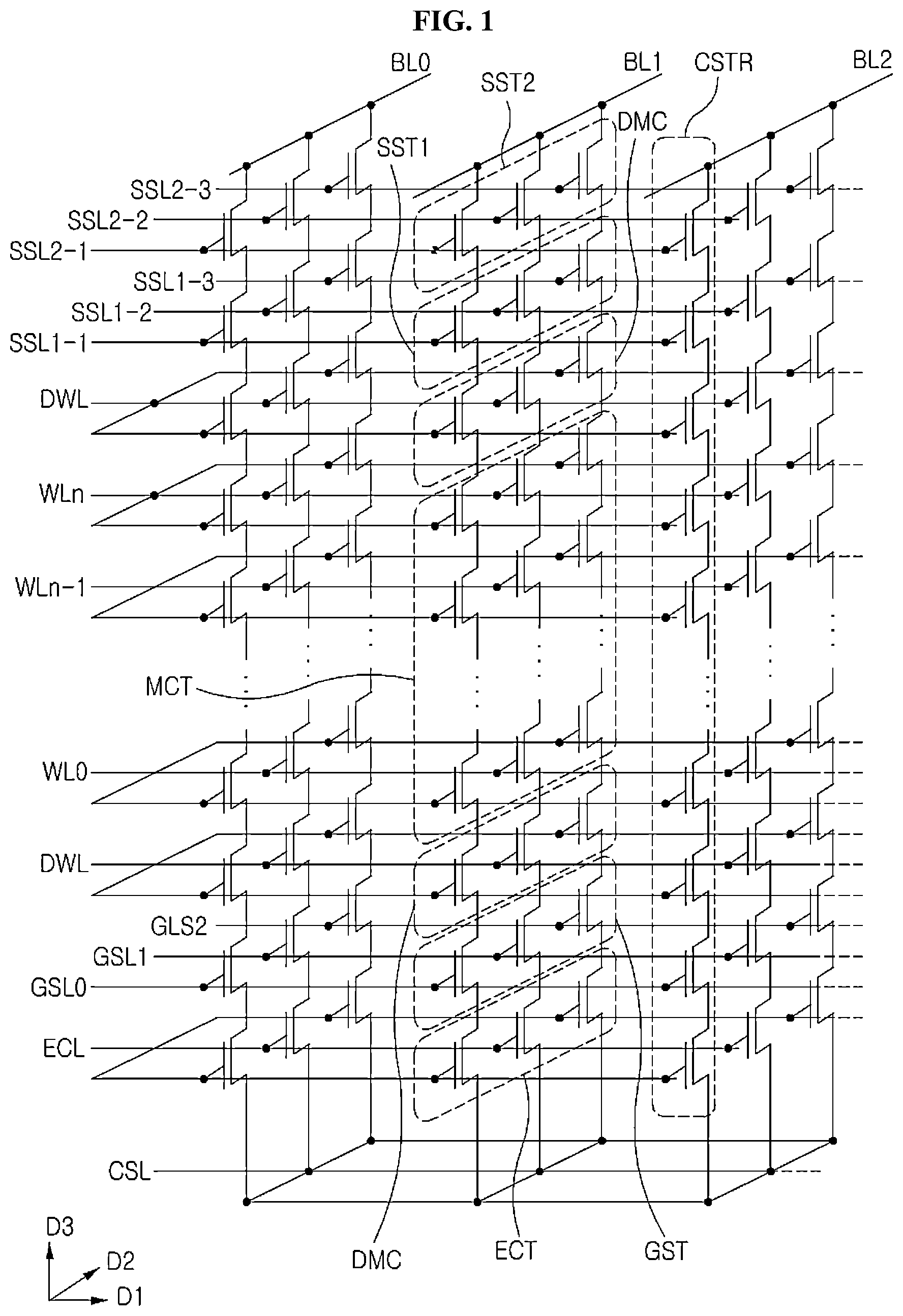
is a schematic circuit diagram illustrating an array of a three-dimensional flash memory according to an embodiment.
is a plan view illustrating a structure of the three-dimensional flash memory according to an embodiment.
is a cross-sectional view illustrating the structure of the three-dimensional flash memory according to an embodiment and corresponds to a cross section along line A-A′ of .
is a flowchart illustrating a program operating method of the three-dimensional flash memory according to an embodiment.
are cross-sectional views illustrating a structure of the three-dimensional flash memory to describe the program operating method illustrated in .
is a flowchart illustrating an erasure operating method of the three-dimensional flash memory according to an embodiment.
is a flowchart illustrating a reading operating method of the three-dimensional flash memory according to an embodiment.
BEST MODE
Hereinafter, embodiments of the present disclosure will be described in detail with reference to the accompanying drawing. However, the present disclosure is not restricted or limited by the embodiments. Further, the same reference numerals in each drawing indicate the same components.
Further, terms used in the specification are used to properly express the embodiments of the present disclosure, and the terms may change depending on the intention of a viewer or an operator or customs in the field to which the present disclosure belongs. Therefore, definitions of these terms should be made based on the content throughout the specification. For example, in the specification, a singular form also includes a plural form unless specifically mentioned in a phrase. Further, the term “comprise” and/or “comprising” used herein does not exclude the presence or addition of one or more other components, steps, operations, and/or elements in or to components, steps, operations, and/or elements mentioned above. Further, even though the terms such as first and second are used in the specification to describe various areas, directions, and shapes, the areas, directions, and shapes should not be limited by these terms. These terms are merely used to distinguish one area, direction or shape from another area, direction or shape. Thus, a portion/part referred to as a “first part/portion” in an embodiment may be referred to as a “second part/portion” in another embodiment.
Further, it should be understood that various embodiments of the present disclosure are different from each other but are not necessarily mutually exclusive. For example, specific shapes, specific structures, and specific characteristics described herein may be implemented in another embodiment without departing from the technical spirit and scope of the present disclosure in relation to the embodiment. Further, it should be understood that positions, arrangements, or configurations of individual components in the range of each presented embodiment may be changed without departing from the technical spirit and scope of the present disclosure.
Hereinafter, a method of operating a three-dimensional flash memory including the ferroelectric-based data storage pattern DSP and the back gate BG will be described in detail with reference to the accompanying drawings.
is a schematic circuit diagram illustrating an array of a three-dimensional flash memory according to an embodiment.
Referring to , the array of the three-dimensional flash memory according to the embodiment may include a common source line CSL, a plurality of bit lines BL 0 , BL 1 , and BL 2 , and a plurality of cell strings CSTR arranged between the common source line CSL and the bit lines BL 0 , BL 1 , and BL 2 .
The bit lines BL 0 , BL 1 , and BL 2 may be two-dimensionally arranged while being spaced apart from each other in a first direction D 1 while extending in a second direction D 2 . Here, the first direction D 1 , the second direction D 2 , and a third direction D 3 may be orthogonal to each other and may form a rectangular coordinate system defined by X, Y, and Z axes.
The plurality of cell strings CSTR may be connected in parallel to the bit lines BL 0 , BL 1 , and BL 2 , respectively. The cell strings CSTR may be commonly connected to the common source line CSL while being provided between the bit lines BL 0 , BL 1 , and BL 2 and the one common source line CSL. In this case, a plurality of common source lines CSL may be provided, and the plurality of common source lines CSL may be two-dimensionally arranged while being spaced apart from each other in the second direction D 2 while extending in the first direction D 1 . The same voltage may be electrically applied to the plurality of common source lines CSL, but the present disclosure is not restricted or limited thereto, and different voltages may be applied to the plurality of common source lines CSL as the plurality of common source lines CSL are electrically independently controlled.
The cell strings CSTR may be arranged spaced apart from each other in the second direction D 2 for each bit line while extending in the third direction D 3 . According to an embodiment, each of the cell strings CSTR may include a ground selection transistor GST connected to the common source line CSL, first and second string selection transistors SST 1 and SST 2 connected to the bit lines BL 0 , BL 1 , and BL 2 and connected in series to each other, memory cell transistors MCT arranged between the ground selection transistor GST and the first and second string selection transistors SST 1 and SST 2 and connected in series to each other, and an erasure control transistor ECT. Further, each of the memory cell transistors MCT may include a data storage element.
As an example, each of the cell strings CSTR may include the first and second string selection transistors SST 1 and SST 2 connected in series to each other, and the second string selection transistor SST 2 may be connected to one of the bit lines BL 0 , BL 1 , and BL 2 . However, the present disclosure is not restricted or limited thereto, and each of the cell strings CSTR may include one string selection transistor. As another example, the ground selection transistor GST in each of the cell strings CSTR may include a plurality of metal oxide semiconductor (MOS) transistors connected in series to each other, which is similar to the first and second string selection transistors SST 1 and SST 2 .
The one cell string CSTR may include the plurality of memory cell transistors MCT having different distances from the common source lines CSL. That is, the memory cell transistors MCT may be connected in series to each other while being arranged between the first string selection transistor SST 1 and the ground selection transistor GST in the third direction D 3 . The erasure control transistor ECT may be connected between the ground selection transistor GST and the common source lines CSL. Each of the cell strings CSTR may further include dummy cell transistors DMC connected between the first string selection transistor SST 1 and an uppermost one of the memory cell transistors MCT and between the ground selection transistor GST and a lowermost one of the memory cell transistors MCT.
According to the embodiment, the first string selection transistor SST 1 may be controlled by first string selection lines SSL 1 - 1 , SSL 1 - 2 , and SSL 1 - 3 , and the second string selection transistor SST 2 may be controlled by second string selection lines SSL 2 - 1 , SSL 2 - 2 , and SSL 2 - 3 . The memory cell transistors MCT may be respectively controlled by a plurality of word lines WL 0 to WLn, and the dummy cell transistors DMC may be respectively controlled by dummy word lines DWL. The ground selection transistor GST may be controlled by ground selection lines GSL 0 , GSL 1 , and GSL 2 , and the erasure control transistor ECT may be controlled by an erasure control line ECL. A plurality of erasure control transistors ECT may be provided. The common source lines CSL may be commonly connected to sources of the erasure control transistors ECT.
Gate electrodes of the memory cell transistors MCT, which are provided at substantially the same distance from the common source lines CSL, may be commonly connected to one of the word lines WL 0 to WLn and DWL and thus may be in an equipotential state. However, the present disclosure is not restricted or limited thereto, and even when the gate electrodes of the memory cell transistors MCT are provided at substantially the same level from the common source lines CSL, the gate electrodes provided in different rows or columns may be independently controlled.
The ground selection lines GSL 0 , GSL 1 , and GSL 2 , the first string selection lines SSL 1 - 1 , SSL 1 - 2 , and SSL 1 - 3 , and the second string selection lines SSL 2 - 1 , SSL 2 - 2 , and SSL 2 - 3 may be two-dimensionally arranged while extending in the first direction D 1 and being spaced apart from each other in the second direction D 2 . The ground selection lines GSL 0 , GSL 1 , and GSL 2 , the first string selection lines SSL 1 - 1 , SSL 1 - 2 , and SSL 1 - 3 , and the second string selection lines SSL 2 - 1 , SSL 2 - 2 , and SSL 2 - 3 , which are provided at substantially the same level from the common source lines CSL, may be electrically separated from each other. Further, the erasure control transistors ECT of different cell strings CSTR may be controlled by the common erasure control line ECL. The erasure control transistors ECT may generate gate induced drain leakage (hereinafter, referred to as GIDL) during an operation of erasing a memory cell array. In some embodiments, during the operation of erasing the memory cell array, an erasure voltage may be applied to the bit lines BL 0 , BL 1 , and BL 2 and/or the common source lines CSL, and a gate induced leakage current may be generated in the string selection transistor SST and/or the erasure control transistors ECT.
The string selection line SSL may be expressed as an upper selection line USL, and the ground selection line GSL may be expressed as a lower selection line.
is a plan view illustrating a structure of the three-dimensional flash memory according to the embodiment, and is a cross-sectional view illustrating the structure of the three-dimensional flash memory according to the embodiment and corresponds to a cross section along line A-A′ of .
Referring to , a substrate SUB may be a semiconductor substrate such as a silicon substrate, a silicon-germanium substrate, a germanium substrate, or a monocrystalline epitaxial layer grown on a monocrystalline silicon substrate. The substrate SUB may be doped with first conductivity-type impurities (e.g., P-type impurities).
Laminated structures ST may be arranged on the substrate SUB. The laminated structures ST may be two-dimensionally arranged in the second direction D 2 while extending in the first direction D 1 . Further, the laminated structures ST may be spaced apart from each other in the second direction D 2 .
Each of the laminated structures ST may include gate electrodes EL 1 , EL 2 , and EL 3 alternately laminated in a vertical direction perpendicular to an upper surface of the substrate SUB (e.g., in the third direction D 3 ), and interlayer insulating films ILD. The laminated structures ST may have substantially flat upper surfaces. That is, the upper surfaces of the laminated structures ST may be parallel to the upper surface of the substrate SUB. Hereinafter, the vertical direction means the third direction D 3 or a direction opposite to the third direction D 3 .
Referring back to , each of the gate electrodes EL 1 , EL 2 , and EL 3 may be one of the erasure control line ECL, the ground selection lines GSL 0 , GSL 1 , and GSL 2 , the word lines WL 0 to WLn and DWL, the first string selection lines SSL 1 - 1 , SSL 1 - 2 , and SSL 1 - 3 , and the second string selection lines SSL 2 - 1 , SSL 2 - 2 , and SSL 2 - 3 that are sequentially laminated on the substrate SUB.
Each of the gate electrodes EL 1 , EL 2 , and EL 3 may have substantially the same thickness in the third direction D 3 while extending in the first direction D 1 . Hereinafter, the thickness means a thickness in the third direction D 3 . Each of the gate electrodes EL 1 , EL 2 , and EL 3 may be formed of a conductive material. For example, each of the gate electrodes EL 1 , EL 2 , and EL 3 may include at least one selected from a doped semiconductor (e.g., a doped silicon or the like), a metal (e.g., W (tungsten), Cu (copper), Al (aluminum), Ti (titanium), Ta (tantalum), Mo (molybdenum), Ru (ruthenium), Au (gold), or the like), a conductive metal nitride (e.g., a titanium nitride, a tantalum nitride, or the like) or the like. Each of the gate electrodes EL 1 , EL 2 , and EL 3 may include at least one of all metal materials that may be formed by ALD in addition to the metal material described above.
In more detail, the gate electrodes EL 1 , EL 2 , and EL 3 may include the lowermost first gate electrode EL 1 , the uppermost third gate electrode EL 3 , and the plurality of second gate electrodes EL 2 between the first gate electrode EL 1 and the third gate electrode EL 3 . Although each of the first gate electrode EL 1 and the third gate electrode EL 3 is illustrated and described in a singular number, this is illustrative, and the present disclosure is not limited thereto. As needed, the plurality of first gate electrodes EL 1 and the plurality of third gate electrodes EL 3 may also be provided. The first gate electrode EL 1 may correspond to one of the ground selection lines GSL 0 , GSL 1 , and GSL 2 illustrated in . The second gate electrode EL 2 may correspond to any one of the word lines WL 0 to WLn and DWL illustrated in . The third gate electrode EL 3 may correspond to any one of the first string selection lines SSL 1 - 1 , SSL 1 - 2 , and SSL 1 - 3 or any one of the second string selection lines SSL 2 - 1 , SSL 2 - 2 , and SSL 2 - 3 illustrated in .
Although not illustrated, an end of each of the laminated structures ST may have a stepwise structure in the first direction D 1 . In more detail, the lengths of the gate electrodes EL 1 , EL 2 , and EL 3 of the laminated structures ST in the first direction D 1 may decrease as a distance from the substrate SUB increases. The third gate electrode EL 3 may have the smallest length in the first direction D 1 and the largest distance from the substrate SUB in the third direction D 3 . The first gate electrode EL 1 may have the largest length in the first direction D 1 and the smallest distance from the substrate SUB in the third direction D 3 . Due to the stepwise structure, the thickness of each of the laminated structures ST may decrease as the distance from the outermost one of vertical channel structures VS, which will be described below, increases, and the side walls of the gate electrodes EL 1 , EL 2 , and EL 3 may be spaced apart from each other at regular intervals in the first direction D 1 when viewed from a plane.
The interlayer insulating films ILD may have different thicknesses. As an example, the lowermost one and the uppermost one of the interlayer insulating films ILD may have a thickness that is smaller than those of the other interlayer insulating films ILD. However, this is illustrative, and the present disclosure is not limited thereto. The interlayer insulating films ILD may be set to have different thickness or the same thickness according to characteristics of a semiconductor device. The interlayer insulating films ILD may be formed of an insulating material to insulate the gate electrodes EL 1 , EL 2 , and EL 3 from each other. As an example, the interlayer insulating films ILD may be formed of a silicon oxide.
A plurality of channel holes CH passing through portions of the laminated structures ST and the substrate SUB may be provided. The vertical channel structures VS may be provided in the channel holes CH. The vertical channel structures VS, which are the plurality of cell strings CSTR illustrated in , may extend in the third direction D 3 while being connected to the substrate SUB. The connection of the vertical channel structures VS with the substrate SUB may be achieved as a lower surface of a portion of each of the vertical channel structures VS is in contact with the upper surface of the substrate SUB, but the present disclosure is not restricted or limited thereto, and the connection of the vertical channel structures VS with the substrate SUB may be achieved as the vertical channel structures VS are buried in the substrate SUB. When portions of the vertical channel structures VS are buried in the substrate SUB, lower surfaces of the vertical channel structures VS may be positioned at a lower level than that of the upper surface of the substrate SUB.
A plurality of columns of the vertical channel structures VS passing through any one of the laminated structures ST may be provided. For example, as illustrated in , the columns of the two vertical channel structures VS may pass through one of the laminated structures ST. However, the present disclosure is not restricted or limited thereto. For example, the columns of the three or more vertical channel structures VS may pass through one of the laminated structures ST. In a pair of adjacent columns, the vertical channel structures VS corresponding to one column may be shifted in the first direction D 1 from the vertical channel structures VS corresponding to the other column adjacent thereto. When viewed from a plane, the vertical channel structures VS may be arranged in a zigzag shape in the first direction D 1 . However, the present disclosure is not restricted or limited thereto, and the vertical channel structures VS may form an array in which the vertical channel structures VS are arranged side by side in rows and columns.
Each of the vertical channel structures VS may be formed to extend from the substrate SUB in the third direction D 3 . In the drawing, each of the vertical channel structures VS is illustrated as having a column shape having the same width at an upper end and a lower end thereof, but the present disclosure is not restricted or limited thereto, and each of the vertical channel structures VS may have a shape of which widths in the first direction D 1 and the second direction D 2 increase toward the third direction D 3 . An upper surface of each of the vertical channel structures VS may have a circular shape, an elliptical shape, a quadrangular shape, or a bar shape.
Each of the vertical channel structures VS may include the data storage pattern DSP, a vertical channel pattern VCP, the back gate BG, and a conductive pad PAD. In each of the vertical channel structures VS, the data storage pattern DSP and the vertical channel pattern VCP may have a pipe shape or a macaroni shape having an open lower end, and the back gate BG may have a shape that fills an inner space of the vertical channel pattern VCP while at least a portion thereof is surrounded by the vertical channel pattern VCP.
While covering inner walls of the channel holes CH, the data storage pattern DSP may inwardly surround an outer wall of the vertical channel pattern VCP and may be outwardly in contact with the side walls of the gate electrodes EL 1 , EL 2 , and EL 3 . Accordingly, areas of the data storage pattern DSP, which correspond to the second gate electrodes EL 2 , together with areas of the vertical channel pattern VCP, which correspond to the second gate electrodes EL 2 , may constitute memory cells in which a memory operation (e.g., a program operation, a reading operation, or an erasure operation) is performed by voltages applied through the second gate electrodes EL 2 . The memory cells correspond to the memory cell transistors MCT illustrated in . To this end, the data storage pattern DSP may be formed of a ferroelectric material to represent data values of charges in the polarization state by the voltages applied through the second gate electrodes EL 2 . As an example, the ferroelectric-based data storage pattern DSP may represent binary data values or multi-valued data values of the charges in the polarization state. Hereinafter, the ferroelectric material may include at least one of HfO x , Pb(Zr, Ti)O 3 , (PZT), PbTiO 3 (PTO), SrBi 2 Ti 2 O 3 (SBT), Bi(La, Ti)O 3 (BLT), Pb(La, Zr)TiO 3 (PLZT), Bi(Sr, Ti)O 3 (BST), barium titanate (BaTiO 3 ), P(VDF-TrFE), PVDF, AlO x , ZnO x , TiO x , TaO x or InO x that is doped with at least one material of HfO x , Al, Zr or Si having an orthorhombic crystal structure.
The vertical channel pattern VCP may cover the inner side wall of the data storage pattern DSP and may extend in the third direction D 3 . The vertical channel pattern VCP may be provided between the data storage pattern DSP and the back gate BG and may constitute the memory cells together with areas of the data storage pattern DSP, which correspond to the second gate electrodes EL 2 .
The upper surface of the vertical channel pattern VCP may be positioned to be higher in level than the upper surface of the uppermost one of the second gate electrodes EL 2 . In more detail, the upper surface of the vertical channel pattern VCP may be positioned between the upper surface and the lower surface of the third gate electrode EL 3 .
The vertical channel pattern VCP, which is a component for transferring charges or holes to the data storage pattern DSP, may be formed of monocrystalline silicon or polysilicon such that the channel is formed or boosted by the voltage applied thereto. However, the present disclosure is not restricted or limited thereto. For example, the vertical channel pattern VCP may be formed of an oxide semiconductor material capable of blocking, suppressing, or minimizing a leakage current. For example, the vertical channel pattern VCP may be formed of an oxide semiconductor material including at least one of In, Zn, and Ga having excellent leakage current characteristics, or a group 4 semiconductor material. The vertical channel pattern VCP may be formed of, for example, a ZnO x -based material including AZO, ZTO, IZO, ITO, IGZO, or Ag—ZnO. Thus, the vertical channel pattern VCP may block, suppress, or minimize a leakage current to the gate electrodes EL 1 , EL 2 , and EL 3 or the substrate SUB, may improve transistor characteristics (e.g., a threshold voltage distribution and a program/read operation speed) of at least one of the gate electrodes EL 1 , EL 2 , and EL 3 , and as a result, may improve electrical characteristics of the three-dimensional flash memory.
The back gate BG may be in contact with the vertical channel pattern VCP, with at least a portion thereof surrounded by the vertical channel pattern VCP, and may be formed to apply a voltage to the vertical channel pattern VCP for the memory operation. To this end, the back gate BG may be formed of a conductive material including at least one selected from the group of doped semiconductor (e.g., doped silicon, etc.), metal (e.g., tungsten (W), copper (Cu), aluminum (Al), titanium (Ti), tantalum (Ta), molybdenum (Mo), ruthenium (Ru), gold (Au), etc.), or conductive metal nitride (e.g., titanium nitride, tantalum nitride, etc.). The back gate BG may include at least one of all metal materials capable of being formed by ALD, in addition to the above-described metal materials.
In this case, the back gate BG may be formed to extend in the third direction D 3 in the vertical channel pattern VCP from a level corresponding to the first gate electrode EL 1 to a level corresponding to the second gate electrode EL 2 . That is, the upper surface of the back gate BG may be positioned to be higher in level than the upper surface of the uppermost one of the second gate electrodes EL 2 . However, the present disclosure is not restricted or limited thereto. For example, the back gate BG may be formed to extend in the third direction D 3 in the vertical channel pattern VCP to a level corresponding to the third gate electrode EL 3 .
A lower substrate in contact with the lower portion of the back gate BG is omitted in the drawing, but depending on an implementation example, the lower substrate in contact with the lower surface of the back gate BG may be included. Further, depending on the implementation example, the back gate BG may be formed from an interior of the substrate SUB or may be formed from an upper portion of the substrate SUB.
The back gate BG may be included in the vertical channel pattern VCP of each of the cell strings CSTR, and all the back gates BG respectively included in the vertical channel patterns VCP of the cell strings CSTR may be electrically connected on a plane formed by the first direction D 1 and the second direction D 2 . That is, the back gate BG may be connected in common to the cell strings CSTR. In this case, the back gates BG of the cell strings CSTR may be collectively controlled such that the same voltage may be applied to all the back gates BG.
However, the present disclosure is not restricted or limited thereto. For example, the back gates BG respectively included in the vertical channel patterns VCP of the cell strings CSTR may be electrically connected to each other in the first direction D 1 of . In this case, the back gates BG of the cell strings CSTR arranged in the second direction D 2 may be electrically controlled independently of each other such that different voltages may be applied to the back gates BG, and the back gates BG of the cell strings CSTR arranged in the first direction D 1 of may be collectively controlled such that the same voltage may be applied to the back gates BG.
Further, the back gates BG respectively included in the vertical channel patterns VCP of the cell strings CSTR may be electrically connected to each other in the second direction D 2 of . In this case, the back gates BG of the cell strings CSTR arranged in the first direction D 1 may be electrically controlled independently of each other such that different voltages are applied to the back gates BG, and the back gates BG of the cell strings CSTR arranged in the second direction D 2 of may be collectively controlled such that the same voltage is applied to the back gates BG.
An insulating film INS may be disposed between the back gate BG and the vertical channel pattern VCP, and thus, the back gate BG may be prevented from being in direct contact with the vertical channel pattern VCP. The insulating film INS may be formed of an insulating material such as a silicon oxide, which is similar to the interlayer insulating films ILD. However, the insulating film INS may be omitted depending on the implementation example.
A structure in which the back gate BG is formed in an internal hole of the vertical channel pattern VCP and is formed in a state of being closely surrounded by the vertical channel pattern VCP is described above, but the present disclosure is not restricted or limited thereto. For example, a structure in which only at least a portion of the back gate BG may be surrounded by the vertical channel pattern VCP may be formed. For example, a structure in which the back gate BG and the insulating film INS are included in at least a portion of the vertical channel pattern VCP or a structure in which the back gate BG and the insulating film INS penetrate the vertical channel pattern VCP may be implemented.
The back gate BG having this structure may be used to apply a voltage to change and maintain states of charges of the ferroelectric-based data storage pattern DSP in a memory operation (e.g., the program operation, the erasure operation, and the reading operation) of the three-dimensional flash memory. Accordingly, a voltage applied to the back gate BG causes the memory operation of the three-dimensional flash memory together with voltages applied to the word lines WL 0 to WLn and voltages applied to the bit lines BL 0 to BL 1 connected to the vertical channel structures VS. Thus, the three-dimensional flash memory according to the embodiment further uses the back gate BG in addition to the word lines WL 0 to WLn and the bit lines BL 0 to BL 1 in the memory operation, and thus a memory operation speed is increased, and cell characteristics and reliability may be improved. A detailed description thereof will be made below.
Referring back to , the vertical channel structures VS may correspond to channels of the erasure control transistor ECT, the first and second string selection transistors SST 1 and SST 2 , the ground selection transistor GST, and the memory cell transistors MCT.
The conductive pad PAD may be provided on the upper surface of the vertical channel pattern VCP. The conductive pad PAD may be connected to an upper portion of the vertical channel pattern VCP. A side wall of the conductive pad PAD may be surrounded by the data storage pattern DSP. An upper surface of the conductive pad PAD may be substantially coplanar with an upper surface of each of the laminated structures ST (i.e., an upper surface of the uppermost one of the interlayer insulating films ILD). A lower surface of the conductive pad PAD may be positioned at a lower level than that of an upper surface of the third gate electrode EL 3 . In more detail, the lower surface of the conductive pad PAD may be positioned between the upper surface and the lower surface of the third gate electrode EL 3 . That is, at least a portion of the conductive pad PAD may overlap the third gate electrode EL 3 in a horizontal direction.
The conductive pad PAD may be formed of a semiconductor doped with impurities or a conductive material. For example, the conductive pad PAD may be formed of a semiconductor material doped with impurities different from that of the substrate SUB (in detail, impurities of a second conductive type (e.g., N-type) different from the first conductive type (e.g., P-type)).
The conductive pad PAD may reduce a contact resistance between the bit line BL, which will be described below, and the vertical channel pattern VCP.
A separation trench TR extending in the first direction D 1 may be provided between the adjacent laminated structures ST. A common source area CSR may be provided inside the substrate SUB exposed by the separation trench TR. The common source area CSR may extend in the first direction D 1 within the substrate SUB. The common source area CSR may be formed of a semiconductor material doped with the second conductive type impurities (e.g., the N-type impurities). The common source area CSR may correspond to the common source line CSL of .
A common source plug CSP may be provided inside the separation trench TR. The common source plug CSP may be connected to the common source area CSR. The upper surface of the common source plug CSP may be substantially coplanar with the upper surface of each of the laminated structures ST (i.e., the upper surface of the uppermost one of the interlayer insulating films ILD). The common source plug CSP may have a plate shape extending in the first direction D 1 and the third direction D 3 . In this case, the common source plug CSP may have a shape of which a width in the second direction D 2 increases toward the third direction D 3 .
Insulation spacers SP may be interposed between the common source plug CSP and the laminated structures ST. The insulation spacers SP may be provided between the adjacent laminated structures ST to face each other. For example, the insulation spacers SP may be formed of a silicon oxide, a silicon nitride, a silicon oxy nitride, or a low-k material having a low dielectric constant.
A capping insulating film CAP may be provided on the laminated structures ST, the vertical channel structures VS, and the common source plug CSP. The capping insulating film CAP may cover the upper surface of the uppermost one of the interlayer insulating films ILD, the upper surface of the conductive pad PAD, and the upper surface of the common source plug CSP. The capping insulating film CAP may be formed of an insulating material different from that of the interlayer insulating films ILD. A bit line contact plug BLPG electrically connected to the conductive pad PAD may be provided inside the capping insulating film CAP. The bit line contact plug BLPG may have a shape of which widths in the first direction D 1 and the second direction D 2 increase toward the third direction D 3 .
The bit line BL may be provided on the capping insulating film CAP and the bit line contact plug BLPG. The bit line BL corresponds to any one of the plurality of bit lines BL 0 , BL 1 , and BL 2 illustrated in and may be formed of a conductive material to extend in the second direction D 2 . The conductive material constituting the bit line BL may be the same material as the conductive material forming each of the gate electrodes EL 1 , EL 2 , and EL 3 .
The bit line BL may be electrically connected to the vertical channel structures VS through the bit line contact plug BLPG. Here, the fact that the bit line BL is connected to the vertical channel structures VS may mean that the bit line BL is connected to the vertical channel patterns VCP included in the vertical channel structures VS.
The three-dimensional flash memory according to the embodiment is not limited or restricted to the above-described structure and may be implemented in various structures as long as the three-dimensional flash memory includes the vertical channel pattern VCP, the ferroelectric-based data storage pattern DSP, the back gate BG, the gate electrodes EL 1 , EL 2 , and EL 3 , the bit line BL, and the common source line CSL according to the implementation example.
is a flowchart illustrating a program operating method of the three-dimensional flash memory according to the embodiment, and are cross-sectional views illustrating a structure of the three-dimensional flash memory to describe the program operating method illustrated in . In more detail, is a cross-sectional view illustrating the structure of the three-dimensional flash memory to describe the program operating method when the vertical channel pattern is an N type, and is a cross-sectional view illustrating the structure of a three-dimensional flash memory to describe the program operating method when the vertical channel pattern is a P type.
Hereinafter, the described program operating method is assumed to be performed by the three-dimensional flash memory having the structure described above with reference to to 3 .
Referring to , in operation S 410 , the three-dimensional flash memory may apply a program voltage V PGM to a selected word line (Sel WL) corresponding to a target memory cell (Sel memory cell) that is a target of the program operation among the word lines WL 0 to WLn.
In operation S 420 , the three-dimensional flash memory may float each of unselected word lines (Unsel WLs) except for the selected word line (Sel WL) among the word lines WL 0 to WLn.
In operation S 430 , the three-dimensional flash memory may apply the pass voltage V PASS to the back gate BG of the selected vertical channel structure (Sel VS) including the target memory cell (Sel memory cell) among the vertical channel structures VS.
In operation S 440 , the three-dimensional flash memory may perform the program operation for the target memory cell (Sel memory cell) in response to a state in which the program voltage V PGM is applied to the selected word line (Sel WL), each of the unselected word lines (Unsel WLs) floats, and the pass voltage V PASS is applied to the back gate BG.
In this way, instead of applying the pass voltage V PASS to each of the unselected word lines (Unsel WLs), the pass voltage V PASS is applied to the back gate BG, and thus a problem that the program operation of the target memory cell (Sel memory cell) is disturbed according to the pass voltage V PASS applied to each of the unselected word lines (Unsel WLs) may be solved.
The program operation according to each type of the vertical channel pattern VCP will be described in detail based on operations S 410 to S 440 . As illustrated in , when the vertical channel pattern VCP is of N type, in operation S 410 , the three-dimensional flash memory may apply a positive program voltage +V PGM to the selected word line (Sel WL). The positive program voltage +V PGM may have a value between 5 V and 12 V. As an example, the positive program voltage +V PGM may have a value of 5 V. The three-dimensional flash memory may float each of the unselected word lines (Unsel WLs) in operation S 420 and then apply a positive pass voltage +V PASS to the back gate BG of the selected vertical channel structure (Sel VS) in operation S 430 . The positive pass voltage +V PASS may have a value between 5 V and 10 V. As an example, the positive pass voltage +V PASS may have a value of 7 V.
In this case, in operation S 430 , the three-dimensional flash memory may apply a ground voltage (0V) to the bit line (Sel BL) connected to the selected vertical channel structure (Sel VS) including the target memory cell (Sel memory cell) among the vertical channel structures VS and apply a voltage (a positive power supply voltage V CC ; e.g., +2 V) that self-boosts the vertical channel pattern VCP of the unselected vertical channel structure (Unsel VS) to the bit line (Unsel BL) connected to the unselected vertical channel structure (Unsel VS) (a vertical channel structure not including the target memory cell (Sel memory cell)) except for the selected vertical channel structure (Sel VS) among the vertical channel structures VS.
Accordingly, the program operation for the target memory cell (Sel memory cell) may be performed in the vertical channel structures VS in which the vertical channel pattern VCP is of an N type.
On the other hand, as illustrated in , when the vertical channel pattern VCP is of a P type, in operation S 410 , the three-dimensional flash memory may apply a negative program voltage −V PGM to the selected word line (Sel WL). The negative program voltage −V PGM may have a value between −12 V and −5 V. As an example, the negative program voltage −V PGM may have a value of −5 V. The three-dimensional flash memory may float each of the unselected word lines (Unsel WLs) in operation S 420 and then apply a negative pass voltage −V PASS to the back gate BG of the selected vertical channel structure (Sel VS) in operation S 430 . The negative pass voltage −V PASS may have a value between −10 V and −5 V. As an example, the negative pass voltage −V PASS may have a value of −7 V.
In this case, in operation S 430 , the three-dimensional flash memory may apply a ground voltage (0V) to the bit line (Sel BL) connected to the selected vertical channel structure (Sel VS) including the target memory cell (Sel memory cell) among the vertical channel structures VS and apply a voltage (a negative power supply voltage V CC ; e.g., −2 V) that self-boosts the vertical channel pattern VCP of the unselected vertical channel structure (Unsel VS) to the bit line (Unsel BL) connected to the unselected vertical channel structure (Unsel VS) (a vertical channel structure not including the target memory cell (Sel memory cell)) except for the selected vertical channel structure (Sel VS) among the vertical channel structures VS.
Accordingly, the program operation for the target memory cell (Sel memory cell) may be performed in the vertical channel structures VS in which the vertical channel pattern VCP is of an P type.
is a flowchart illustrating an erasure operating method of the three-dimensional flash memory according to the embodiment.
Hereinafter, the described erasure operating method is assumed to be performed by the three-dimensional flash memory having the structure described above with reference to to 3 .
Referring to , in operation S 710 , the three-dimensional flash memory may apply an erasure voltage V ERASE for generating the GIDL with the string selection line SSL to the bit line BL of each of the vertical channel structures VS, which are included in a block that is a target of the erasure operation, among the vertical channel structures VS.
In operation S 720 , the three-dimensional flash memory may apply the ground voltage 0V to each of the word lines WL 0 to WLn.
In operation S 730 , the three-dimensional flash memory may float the back gate BG of each of the vertical channel structures VS included in the block.
In operation S 740 , the three-dimensional flash memory may perform the erasure operation on memory cells of each of the vertical channel structures VS included in the block in response to the GIDL generated in each of the vertical channel structures VS included in the block.
The erasure operation according to each type of the vertical channel pattern VCP will be described in detail based on operations S 710 to S 740 . When the vertical channel pattern VCP is of an N type, in operation S 710 , the three-dimensional flash memory may apply a positive erasure voltage +V ERASE to the bit line BL of each of the vertical channel structures VS included in the block that is a target of the erasure operation. The positive erasure voltage +V ERASE may have a value between 5 V and 12 V. As an example, the positive erasure voltage +V ERASE may have a value of 10 V. Accordingly, the erasure operation may be performed on the vertical channel structures VS in which the vertical channel pattern VCP is of an N type.
On the other hand, when the vertical channel pattern VCP is of a P type, in operation S 710 , the three-dimensional flash memory may apply a negative erasure voltage −V ERASE to the bit line BL of each of the vertical channel structures VS included in the block that is a target of the erasure operation. The negative erasure voltage −V ERASE may have a value between −12 V and −5 V. As an example, the negative erasure voltage −V ERASE may have a value of −10 V. Accordingly, the erasure operation may be performed on the vertical channel structures VS in which the vertical channel pattern VCP is of an P type.
is a flowchart illustrating a reading operating method of the three-dimensional flash memory according to the embodiment.
Hereinafter, the described reading operating method is assumed to be performed by the three-dimensional flash memory having the structure described above with reference to to 3 .
Referring to , in operation S 810 , the three-dimensional flash memory may apply a reading voltage V READ to the selected word line (Sel WL) corresponding to the target memory cell (Sel memory cell) that is a target of the reading operation among the word lines WL 0 to WLn.
In operation S 820 , the three-dimensional flash memory may apply the pass voltage V PASS to each of the unselected word lines (Unsel WLs) except for the selected word line (Sel WL) among the word lines WL 0 to WLn.
In operation S 830 , the three-dimensional flash memory may apply a first voltage V 1 to the bit line (Sel BL) of the selected vertical channel structure (Sel VS) including the target memory cell (Sel memory cell) among the vertical channel structures VS.
In operation S 840 , the three-dimensional flash memory may apply the ground voltage 0V to the back gate BG of the selected vertical channel structure (Sel VS) including the target memory cell (Sel memory cell) among the vertical channel structures VS.
In operation S 850 , the three-dimensional flash memory may perform the reading operation on the target memory cell (Sel memory cell) in response to the reading voltage V READ being applied to the selected word line (Sel WL), the pass voltage V PASS being applied to each of the unselected word lines (Unsel WLs), the first voltage V 1 being applied to the bit line (Sel BL) of the selected vertical channel structure (Sel VS), and the ground voltage 0V being applied to the back gate BG of the selected vertical channel structure (Sel VS).
The reading operation according to each type of the vertical channel pattern VCP will be described in detail based on operations S 810 to S 850 . When the vertical channel pattern VCP is of N type, in operation S 810 , the three-dimensional flash memory may apply a positive reading voltage +V READ to the selected word line (Sel WL). In operation S 820 , the three-dimensional flash memory may apply the positive pass voltage +V PASS (e.g., +2 V) to each of the unselected word lines (Unsel WLs). Further, in operation S 830 , the three-dimensional flash memory may apply a positive first voltage V 1 (e.g., +1 V) to the bit line (Sel BL) of the selected vertical channel structure (Sel VS) including the target memory cell (Sel memory cell) among the vertical channel structures VS and may apply the ground voltage 0V to the bit line (Unsel VS) of the unselected vertical channel structure (Unsel VS) not including the target memory cell (Sel memory cell) among the vertical channel structures VS.
Accordingly, the reading operation for the target memory cell (Sel memory cell) may be performed in the vertical channel structures VS in which the vertical channel pattern VCP is of an N type.
On the other hand, when the vertical channel pattern VCP is of a P type, in operation S 810 , the three-dimensional flash memory may apply a negative reading voltage −V READ to the selected word line (Sel WL). In operation S 820 , the three-dimensional flash memory may apply the negative pass voltage −V PASS (e.g., −2 V) to each of the unselected word lines (Unsel WLs). Further, in operation S 830 , the three-dimensional flash memory may apply a negative first voltage V 1 (e.g., −1 V) to the bit line (Sel BL) of the selected vertical channel structure (Sel VS) including the target memory cell (Sel memory cell) among the vertical channel structures VS and may apply the ground voltage 0V to the bit line (Unsel VS) of the unselected vertical channel structure (Unsel VS) not including the target memory cell (Sel memory cell) among the vertical channel structures VS.
Accordingly, the reading operation for the target memory cell (Sel memory cell) may be performed in the vertical channel structures VS in which the vertical channel pattern VCP is of an P type.
As described above, although the embodiments have been described with reference to the limited embodiments and the limited drawings, various modifications and changes may be made based on the above description by those skilled in the art. For example, even though the described technologies are performed in an order different from the described method, and/or the described components such as a system, a structure, a device, and a circuit are coupled or combined in a form different from the described method or are replaced or substituted by other components or equivalents, appropriate results may be achieved.
Therefore, other implementations, other embodiments, and those equivalent to the appended claims also belong to the scope of the appended claims.
Figures (8)
Citations
This patent cites (9)
- US9805807
- US10210921
- US2017/0076808
- US2020/0381061
- US2021/0398593
- US2022/0013533
- US10-2014-0086599
- US10-2017-0019541
- US10-2017-0093099