Semiconductor Module Including a Clip Structure
Abstract
Disclosed is a semiconductor module comprising a module substrate having a top surface and a bottom surface that are opposite to each other, a plurality of semiconductor packages on the top surface of the module substrate and arranged in a first direction parallel to the top surface of the module substrate, and a clip structure on the top surface of the module substrate and spaced apart from the plurality of semiconductor packages in the first direction. The clip structure includes a body part on the top surface of the module substrate and spaced apart from the plurality of semiconductor packages in the first direction, and a connection part that extends from the body part across a lateral surface of the module substrate onto the bottom surface of the module substrate.
Claims (18)
1 . A semiconductor module, comprising: a module substrate having a top surface and a bottom surface that are opposite to each other; a plurality of semiconductor packages on the top surface of the module substrate and arranged in a first direction parallel to the top surface of the module substrate; a clip structure on the top surface of the module substrate and spaced apart from the plurality of semiconductor packages in the first direction, and a plurality of tabs on the top surface of the module substrate and arranged in the first direction at a first side of the module substrate, wherein the plurality of tabs are spaced apart in a second direction from the plurality of semiconductor packages and the clip structure, wherein the second direction is parallel to the top surface of the module substrate and intersects the first direction, wherein the clip structure comprises: a body part on the top surface of the module substrate and spaced apart from the plurality of semiconductor packages in the first direction; and a connection part that extends from the body part across a lateral surface of the module substrate onto the bottom surface of the module substrate.
11 . A semiconductor module, comprising: a module substrate having a top surface and a bottom surface that are opposite to each other, the module substrate comprising: a first side and a second side that extend in a first direction and are opposite to each other, and a third side and a fourth side that extend in a second direction and are opposite to each other, wherein the first direction and the second direction are parallel to the top surface of the module substrate and intersect each other; a plurality of semiconductor packages on the top surface of the module substrate and arranged in the first direction; a plurality of tabs on the top surface of the module substrate, adjacent to the first side, and arranged in the first direction; and a clip structure on the top surface of the module substrate and spaced apart from the plurality of semiconductor packages and the plurality of tabs in the first direction, wherein the plurality of tabs are spaced apart in the second direction from the plurality of semiconductor packages and the clip structure, wherein the clip structure comprises: a body part on the top surface of the module substrate, the body part extending in the second direction between an outermost one of the plurality of semiconductor packages and the third side of the module substrate; and a connection part adjacent to the second side of the module substrate, the connection part extending from the body part across a lateral surface of the module substrate onto the bottom surface of the module substrate.
18 . A semiconductor module, comprising: a module substrate having a top surface and a bottom surface that are opposite to each other; a plurality of semiconductor packages on the top surface of the module substrate; and a clip structure on the top surface of the module substrate and spaced apart from the plurality of semiconductor packages in a first direction, wherein the clip structure comprises: a body part on the top surface of the module substrate and spaced apart from the plurality of semiconductor packages in the first direction; and a connection part that extends from the body part onto the bottom surface of the module substrate and is in direct contact with a lateral surface of the module substrate, wherein the lateral surface of the module substrate is on an outer edge of the clip structure in a second direction that intersects the first direction, and wherein the body part comprises a curved surface remote from the plurality of semiconductor packages.
Show 15 dependent claims
2 . The semiconductor module of claim 1 , wherein the connection part of the clip structure is adjacent to a second side of the module substrate, and wherein the first side and the second side of the module substrate are opposite to each other.
3 . The semiconductor module of claim 1 , further comprising: a plurality of semiconductor elements on the top surface of the module substrate, wherein the clip structure is spaced apart from the plurality of semiconductor elements in the first direction.
4 . The semiconductor module of claim 1 , wherein respective ones of the plurality of semiconductor packages comprises: a package substrate; a semiconductor chip on the package substrate; and a molding layer on the package substrate, wherein the molding layer is on the semiconductor chip.
5 . The semiconductor module of claim 1 , wherein the clip structure is electrically isolated from the plurality of semiconductor packages.
6 . The semiconductor module of claim 1 , wherein the body part of the clip structure has a bar shape that extends in the second direction at one side of an outermost one of the plurality of semiconductor packages.
7 . The semiconductor module of claim 6 , wherein the body part comprises: a first lateral surface that faces the outermost one of the plurality of semiconductor packages; and a second lateral surface opposite to the first lateral surface, wherein the second lateral surface of the body part has a curved surface, an angled surface, or a plate shape that is inclined relative to the top surface of the module substrate.
8 . The semiconductor module of claim 1 , wherein the module substrate comprises: the first side and a second side that extend in the first direction and are opposite to each other; and a third side and a fourth side that extend in the second direction and are opposite to each other, wherein the body part of the clip structure comprises: a first body part that extends in the second direction between a first outermost one of the plurality of semiconductor packages and the third side of the module substrate; and a second body part that extends in the first direction at one side of the plurality of semiconductor packages, wherein the first body part and the second body part are connected to each other on the top surface of the module substrate in an L shape.
9 . The semiconductor module of claim 8 , wherein the body part of the clip structure further comprises: a third body part that extends in the second direction between a second outermost one of the plurality of semiconductor packages and the fourth side of the module substrate; and a fourth body part that extends in the second direction between the plurality of semiconductor packages, wherein the first body part, the second body part, the third body part, and the fourth body part are connected to each other on the top surface of the module substrate in an E shape.
10 . The semiconductor module of claim 1 , wherein the plurality of semiconductor packages on the top surface of the module substrate are upper semiconductor packages, wherein the body part on the top surface of the module substrate is an upper body part, wherein the semiconductor module further comprises a plurality of lower semiconductor packages on the bottom surface of the module substrate, wherein the clip structure further comprises a lower body part on the bottom surface of the module substrate and spaced apart from the lower semiconductor packages in the first direction, and wherein the connection part extends from the upper body part to the lower body part.
12 . The semiconductor module of claim 11 , wherein the body part comprises: a first lateral surface that faces the outermost one of the plurality of semiconductor packages; and a second lateral surface opposite to the first lateral surface, wherein the second lateral surface of the body part has a curved surface, an angled surface, or a plate shape that is inclined relative to the top surface of the module substrate.
13 . The semiconductor module of claim 12 , wherein the second lateral surface of the body part comprises a plurality of curved surfaces that are different from each other.
14 . The semiconductor module of claim 11 , wherein, when viewed from the second side of the module substrate, the body part has a half-streamline shaped sidewall, a half-dolphin shaped sidewall, a rectangular sidewall, or a triangular sidewall.
15 . The semiconductor module of claim 11 , wherein the body part comprises a first body part, wherein the clip structure further comprises a second body part on the top surface of the module substrate and adjacent to the second side of the module substrate, the second body part extending in the first direction at one side of the plurality of semiconductor packages, and wherein the first body part and the second body part are connected to each other on the top surface of the module substrate in an L shape in plan view.
16 . The semiconductor module of claim 15 , wherein the outermost one of the plurality of semiconductor packages is a first outermost semiconductor package, wherein the clip structure further comprises: a third body part on the top surface of the module substrate, the third body part extending in the second direction between a second outermost one of the plurality of semiconductor packages and the fourth side of the module substrate; and a fourth body part that extends in the second direction between the plurality of semiconductor packages, and wherein the first body part, the second body part, the third body part, and the fourth body part are connected to each other on the top surface of the module substrate in an E shape in plan view.
17 . The semiconductor module of claim 11 , wherein the clip structure comprises a non-conductive material or is electrically isolated from the plurality of semiconductor packages.
Full Description
Show full text →
CROSS-REFERENCE TO RELATED APPLICATION
This U.S. nonprovisional application claims priority under 35 U.S.C § 119 to Korean Patent Application No. 10-2021-0193230 filed on Dec. 30, 2021 in the Korean Intellectual Property Office, the disclosure of which is hereby incorporated by reference in its entirety.
BACKGROUND
The present inventive concepts relate to a semiconductor module, and more particularly, to a semiconductor module including memory packages. A data center is increasingly utilized due to explosive growth of internet, artificial intelligence, cloud computing, and high performance computing (HPC), and immersion cooling is utilized to effectively cool computing hardware included in the data center. The immersion cooling is a cooling practice by which computing hardware is submerged in a non-conductive liquid, and may reduce the need for cooling components such as thermal interface material, heat sinks, and/or fans. The immersion cooling is classified into single-phase immersion cooling and two-phase immersion cooling. As regards the two-phase immersion cooling, heat generated from computing hardware may cause a coolant to change from its liquid state into a gaseous state, which may result in the occurrence of vapor. The two-phase immersion cooling may achieve effective cooling compared to the single-phase immersion cooling, but vapor produced during cooling may problematically deteriorate reliability of semiconductor modules.
SUMMARY
Some embodiments of the present inventive concepts provide a semiconductor module capable of preventing vapor from being trapped and easily transferring heat in two-phase immersion cooling. Some embodiments of the present inventive concepts provide a semiconductor module with increased reliability. According to some embodiments of the present inventive concepts, a semiconductor module may include a module substrate having a top surface and a bottom surface that are opposite to each other, a plurality of semiconductor packages on the top surface of the module substrate and arranged in a first direction parallel to the top surface of the module substrate, and a clip structure on the top surface of the module substrate and spaced apart from the plurality of semiconductor packages in the first direction. The clip structure may include a body part on the top surface of the module substrate and spaced apart from the plurality of semiconductor packages in the first direction, and a connection part that extends from the body part across a lateral surface of the module substrate onto the bottom surface of the module substrate. According to some embodiments of the present inventive concepts, a semiconductor module may include a module substrate having a top surface and a bottom surface that are opposite to each other, the module substrate having a first side and a second side that extend in a first direction and are opposite to each other, and a third side and a fourth side that extend in a second direction and are opposite to each other, the first direction and second direction are parallel to the top surface of the module substrate and intersect each other, a plurality of semiconductor packages on the top surface of the module substrate and arranged in the first direction, a plurality of tabs on the top surface of the module substrate, adjacent to the first side, and arranged in the first direction; and a clip structure on the top surface of the module substrate and spaced apart from the plurality of semiconductor packages and the plurality of tabs in the first direction. The clip structure may include a body part on the top surface of the module substrate, the body part extending in the second direction between an outermost one of the plurality of semiconductor packages and the third side of the module substrate; and a connection part adjacent to the second side of the module substrate, the connection part extending from the body part across a lateral surface of the module substrate onto the bottom surface of the module substrate. According to some embodiments of the present inventive concepts, a semiconductor module includes a module substrate having a top surface and a bottom surface that are opposite to each other, a plurality of semiconductor packages on the top surface of the module substrate, and a clip structure on the top surface of the module substrate and spaced apart from the plurality of semiconductor packages in a first direction. The clip structure includes a body part on the top surface of the module substrate and spaced apart from the plurality of semiconductor packages in the first direction, and a connection part that extends from the body part onto the bottom surface of the module substrate. The body part includes a curved surface remote from the plurality of semiconductor packages.
BRIEF DESCRIPTION OF THE DRAWINGS
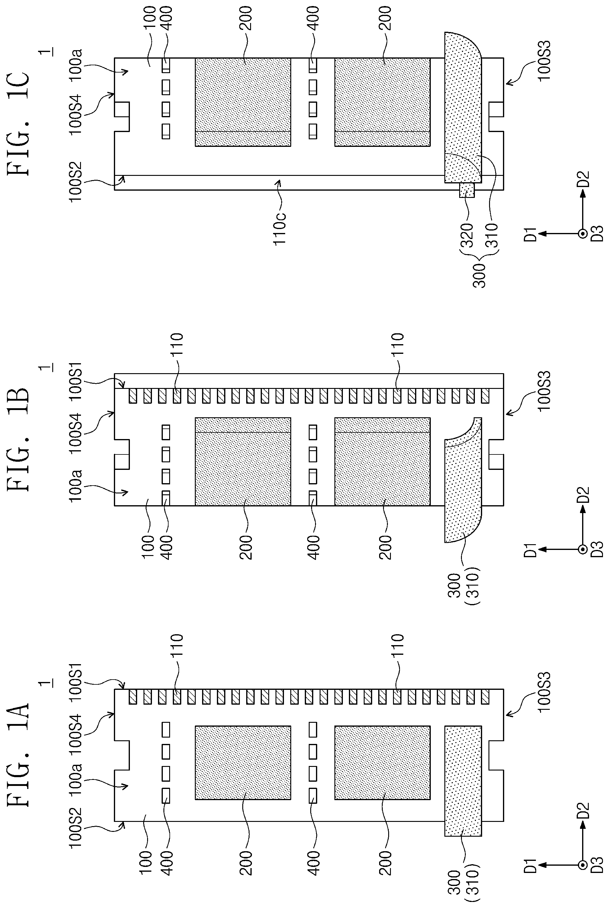
A illustrates a plan view showing a semiconductor module according to some embodiments of the present inventive concepts. B illustrates a perspective view showing a first side of the semiconductor module depicted in A . C illustrates a perspective view showing a second side of the semiconductor module depicted in A . illustrates a cross-sectional view seen from the second side of the semiconductor module depicted in A . illustrates diagrams in accordance with a rotation angle of a clip structure depicted in A . A illustrates a plan view showing a semiconductor module according to some embodiments of the present inventive concepts. B illustrates a perspective view showing a first side of the semiconductor module depicted in A . C illustrates a perspective view showing a second side of the semiconductor module depicted in A . illustrates a cross-sectional view seen from the second side of the semiconductor module depicted in A . A illustrates a plan view showing a semiconductor module according to some embodiments of the present inventive concepts. B illustrates a perspective view showing a first side of the semiconductor module depicted in A . C illustrates a perspective view showing a second side of the semiconductor module depicted in A . illustrates a cross-sectional view seen from the second side of the semiconductor module depicted in A . A illustrates a plan view showing a semiconductor module according to some embodiments of the present inventive concepts. B illustrates a perspective view showing a first side of the semiconductor module depicted in A . C illustrates a perspective view showing a second side of the semiconductor module depicted in A . illustrates a cross-sectional view seen from the second side of the semiconductor module depicted in A . A illustrates a plan view showing a semiconductor module according to some embodiments of the present inventive concepts. B illustrates a perspective view showing a first side of the semiconductor module depicted in A . C illustrates a perspective view showing a second side of the semiconductor module depicted in A . illustrates a cross-sectional view seen from the second side of the semiconductor module depicted in A . A illustrates a plan view showing a semiconductor module according to some embodiments of the present inventive concepts. B illustrates a perspective view showing a first side of the semiconductor module depicted in A . C illustrates a perspective view showing a second side of the semiconductor module depicted in A . illustrates a cross-sectional view seen from the second side of the semiconductor module depicted in A . illustrates a cross-sectional view seen from the second side of the semiconductor module depicted in A according to some embodiments of the present inventive concepts. illustrates diagrams in accordance with a rotation angle of a clip structure depicted in . illustrates a cross-sectional view seen from the second side of the semiconductor module depicted in A according to some embodiments of the present inventive concepts. illustrates a cross-sectional view seen from the second side of the semiconductor module depicted in A according to some embodiments of the present inventive concepts. A illustrates a plan view showing a semiconductor module according to some embodiments of the present inventive concepts. B illustrates a perspective view showing a first side of the semiconductor module depicted in A . C illustrates a perspective view showing a second side of the semiconductor module depicted in A . illustrates a cross-sectional view seen from the second side of the semiconductor module depicted in A . illustrates diagrams in accordance with a rotation angle of a clip structure depicted in A .
DETAILED DESCRIPTION
The following will now describe in detail some embodiments of the present inventive concepts with reference to the accompanying drawings. A illustrates a plan view showing a semiconductor module according to some embodiments of the present inventive concepts. B illustrates a perspective view showing a first side of the semiconductor module depicted in A . C illustrates a perspective view showing a second side of the semiconductor module depicted in A . illustrates a cross-sectional view seen from the second side of the semiconductor module depicted in A . illustrates diagrams in accordance with a rotation angle of a clip structure depicted in A . Referring to A, 1 B, 1 C, and 2 , a semiconductor module 1 may include a module substrate 100 , a plurality of tabs 110 , a plurality of semiconductor packages 200 , a clip structure 300 , and a plurality of semiconductor elements 400 . The module substrate 100 may be a printed circuit board (PCB) with a circuit pattern. The module substrate 100 may have a top surface 100 a and a bottom surface 100 b that are opposite to each other. The module substrate 100 may have a first side 100 S 1 and a second side S 2 that extend in a first direction D 1 and face each other, and may also include a third side 100 S 3 and a fourth side 100 S 4 that extend in a second direction D 2 and face each other. The first direction D 1 and the second direction D 2 may be parallel to the top surface 100 a of the substrate 100 and may be crossed (e.g., orthogonal) to each other. The plurality of tabs 110 may be disposed on the top surface 100 a of the module substrate 100 and adjacent to the first side 100 S 1 . The plurality of tabs 110 may be arranged in the first direction D 1 at the first side 100 S 1 of the module substrate 100 . The plurality of tabs 110 may include metal (e.g., copper or aluminum). The plurality of tabs 110 may have their standardized function and arrangement, and for example, may satisfy JEDEC standards. The plurality of tabs 110 may serve either as input/output terminals for data signals or as transfer paths for command/address (C/A) signals. The plurality of semiconductor packages 200 may be disposed on the top surface 100 a of the module substrate 100 and may be arranged in the first direction D 1 . The plurality of tabs 110 may be spaced apart in the second direction D 2 from the plurality of semiconductor packages 200 . The plurality of semiconductor packages 200 may be electrically connected to the plurality of tabs 110 through wiring lines in the module substrate 100 . Therefore, data signals and command/address signals may be transceived between the plurality of semiconductor packages 200 and the plurality of tabs 110 . Each of the plurality of semiconductor packages 200 may include a package substrate 220 , a semiconductor chip 230 , and a molding layer 240 . The package substrate 220 may be, for example, a printed circuit board (PCB) or a redistribution substrate. The semiconductor chip 230 may be mounted on the package substrate 220 , and may be a memory chip, a logic chip, an application processor (AP) chip, or a system-on-chip (SOC). The package substrate 220 may be provided thereon with the molding layer 240 that encapsulates the semiconductor chip 230 . The plurality of semiconductor packages 200 may be memory packages, and in this case, the semiconductor chip 230 may be a memory chip. The semiconductor chip 230 may include, for example, dynamic random access memory (DRAM), static random access memory (SRAM), or synchronous dynamic random access memory (SDRAM). Connection terminals 210 may be interposed between the module substrate 100 and each of the plurality of semiconductor packages 200 . Each of the plurality of semiconductor packages 200 may be electrically connected through the connection terminals 210 to the module substrate 100 (e.g., to the wiring lines in the module substrate 100 ). The connection terminals 210 may include at least one selected from pillars, bumps, and solder balls, and may be formed of a conductive material. The semiconductor chip 230 included in each of the plurality of semiconductor packages 200 may be electrically connected through the package substrate 220 and the connection terminals 210 to the module substrate 100 (e.g., to the wiring lines in the module substrate 100 ). The plurality of semiconductor elements 400 may be disposed on the top surface 100 a of the module substrate 100 , and may be horizontally spaced apart from the plurality of semiconductor packages 200 . The plurality of semiconductor elements 400 may include an active element or a passive element (e.g., resistor, capacitor, or inductor). The plurality of semiconductor elements 400 may be electrically connected to the plurality of semiconductor packages 200 through the module substrate 100 (e.g., through the wiring lines in the module substrate 100 ). Referring to A, 1 B, 1 C, 2 , and 3 , the clip structure 300 may be disposed on the top surface 100 a of the module substrate 100 , and may be horizontally spaced apart from the plurality of semiconductor packages 200 , the plurality of semiconductor elements 400 , and the plurality of tabs 110 . The plurality of tabs 110 may be spaced apart in the second direction D 2 from the clip structure 300 . The clip structure 300 may be disposed on the top surface 100 a of the module substrate 100 . The clip structure 300 may include a body part 310 that is horizontally spaced apart from the plurality of semiconductor packages 200 , the plurality of semiconductor elements 400 , and the plurality of tabs 110 , and may also include a connection part 320 that extends from the body part 310 across a lateral surface 100 c of the module substrate 100 onto the bottom surface 100 b of the module substrate 100 . The connection part 320 of the clip structure 300 may be disposed adjacent to the second side 100 S 2 of the module substrate 100 , and the body part 310 of the clip structure 300 may be spaced apart in the second direction D 2 from the plurality of tabs 110 . According to some embodiments, the body part 310 of the clip structure 300 may be placed between an outermost one of the plurality of semiconductor packages 200 and the third side 100 S 3 of the module substrate 100 . Among the plurality of semiconductor packages 200 , the outermost semiconductor package 200 may be a semiconductor package that is adjacent to or closest to the third side 100 S 3 of the module substrate 100 . The body part 310 may have a bar shape that extends in the second direction D 2 between the outermost semiconductor package 200 and the third side 100 S 3 of the module substrate 100 . The body part 310 may have a first lateral surface 310 S 1 that faces the outermost semiconductor package 200 and a second lateral surface 310 S 2 that stands opposite to the first lateral surface 310 S 1 . According to some embodiments, the second lateral surface 310 S 2 of the body part 310 may be a curved surface. When viewed from the second side 100 S 2 of the module substrate 100 , as illustrated in , the body part 310 may have a half-streamline shaped sidewall 310 W. The body part 310 may have a height H in a third direction D 3 perpendicular to the top surface 100 a of the module substrate 100 , and for example, the height H of the body part 310 may range from about 0.01 mm to about 100 mm. A maximum height H of the body part 310 may be substantially the same as a height of an uppermost surface of each of the plurality of semiconductor packages 200 . The body part 310 may have a width W in the first direction D 1 , and for example, the width W of the body part 310 may range from 0.01 mm to about 200 mm. The body part 310 may have a length L in the second direction D 2 , and for example, the length L of the body part 310 may range from about 0.01 mm to about 200 mm. The connection part 320 may include a first portion P 1 that extends from the sidewall 310 W of the body part 310 onto the top surface 100 a of the module substrate 100 , a second portion P 2 that extends from the first portion P 1 onto the lateral surface 100 c of the module substrate 100 , and a third portion P 3 that extends from the second portion P 2 onto the bottom surface 100 b of the module substrate 100 . The module substrate 100 may be inserted into between the first and third portions P 1 and P 3 of the connection part 320 , and accordingly, the clip structure 300 may be physically attached to the module substrate 100 . The clip structure 300 may include a non-conductive material. For example, the clip structure 300 may be formed of one or more of plastics, fiber, rubber, sponge, urethane, carbon materials, and/or porous materials. The clip structure 300 may be electrically separated from or signal isolated from the plurality of semiconductor packages 200 , the plurality of tabs 110 , and the plurality of semiconductor elements 400 . When two-phase immersion cooling is employed to cool the semiconductor module 1 , vapor produced due to a state change of a non-conductive coolant may be trapped between the module substrate 100 and each of the plurality of semiconductor packages 200 . In this case, a low thermal conductivity of the vapor may interrupt heat transfer from the plurality of semiconductor packages 200 to the non-conductive coolant, and thus the semiconductor module 1 may decrease in reliability. According to the present inventive concepts, the clip structure 300 may change a flow of vapor produced in two-phase immersion cooling. For example, the vapor produced in two-phase immersion cooling may ascend along the first direction D 1 , and the clip structure 300 may change a flow path of the vapor. Accordingly, the vapor may be suppressed from being trapped between the module substrate 100 and each of the plurality of semiconductor packages 200 , and the non-conductive coolant with high thermal conductivity may fill or at least partially occupy a space between the module substrate 100 and each of the plurality of semiconductor packages 200 . As a result, heat may be easily transferred from the plurality of semiconductor packages 200 to the non-conductive coolant, and therefore the production of semiconductor module 1 may increase in reliability. In addition, as the second lateral surface 310 S 2 of the body part of the clip structure 300 is shaped like a curved surface, it may be possible to improve fluidity of the non-conductive coolant used in two-phase immersion cooling. A illustrates a plan view showing a semiconductor module according to some embodiments of the present inventive concepts. B illustrates a perspective view showing a first side of the semiconductor module depicted in A . C illustrates a perspective view showing a second side of the semiconductor module depicted in A . illustrates a cross-sectional view seen from the second side of the semiconductor module depicted in A . In the embodiment that follows, differences from the semiconductor module described with reference to A, 1 B, 1 C, 2 , and 3 will be mainly discussed herein in the interest of brevity. Referring to A, 4 B, 4 C, and 5 , the body part 310 of the clip structure 300 may have a first lateral surface 310 S 1 that faces the outermost semiconductor package 200 and a second lateral surface 310 S 2 that stands opposite to the first lateral surface 310 S 1 . According to some embodiments, the second lateral surface 301 S 2 of the body part 310 may be a curved surface, and may have a plurality of curvatures different from each other. For example, the second lateral surface 310 S 2 of the body part 310 may be a curved surface having two different curvatures. When viewed from the second side 100 S 2 of the module substrate 100 , as illustrated in , the body part 310 may have a half-dolphin shaped sidewall 310 W. According to some embodiments, as the second lateral surface 310 S 2 of the body part of the clip structure 300 is shaped like a curved surface having a plurality of curvatures different from each other, it may be possible to improve fluidity of the non-conductive coolant used in two-phase immersion cooling. A illustrates a plan view showing a semiconductor module according to some embodiments of the present inventive concepts. B illustrates a perspective view showing a first side of the semiconductor module depicted in A . C illustrates a perspective view showing a second side of the semiconductor module depicted in A . illustrates a cross-sectional view seen from the second side of the semiconductor module depicted in A . In the embodiment that follows, differences from the semiconductor module described with reference to A, 1 B, 1 C, 2 , and 3 will be mainly discussed herein in the interest of brevity. Referring to A, 6 B, 6 C, and 7 , the body part 310 of the clip structure 300 may have a first lateral surface 310 S 1 that faces the outermost semiconductor package 200 and a second lateral surface 310 S 2 that stands opposite to the first lateral surface 310 S 1 . According to some embodiments, the second lateral surface 310 S 2 of the body part 310 may be an angled surface. When viewed from the second side 100 S 2 of the module substrate 100 , as illustrated in , the body part 310 may have a rectangular sidewall 310 W. A illustrates a plan view showing a semiconductor module according to some embodiments of the present inventive concepts. B illustrates a perspective view showing a first side of the semiconductor module depicted in A . C illustrates a perspective view showing a second side of the semiconductor module depicted in A . illustrates a cross-sectional view seen from the second side of the semiconductor module depicted in A . In the embodiment that follows, differences from the semiconductor module described with reference to A, 1 B, 1 C, 2 , and 3 will be mainly discussed herein in the interest of brevity. Referring to A, 8 B, 8 C, and 9 , the body part 310 of the clip structure 300 may have a first lateral surface 310 S 1 that faces the outermost semiconductor package 200 and a second lateral surface 310 S 2 that stands opposite to the first lateral surface 310 S 1 . According to some embodiments, the second lateral surface 310 S 2 of the body part 310 may have a plane shape that is inclined to the top surface 100 a of the module substrate 100 . When viewed from the second side 100 S 2 of the module substrate 100 , as illustrated in , the body part 310 may have a triangular (e.g., right-angled triangular) sidewall 310 W. A illustrates a plan view showing a semiconductor module according to some embodiments of the present inventive concepts. B illustrates a perspective view showing a first side of the semiconductor module depicted in A . C illustrates a perspective view showing a second side of the semiconductor module depicted in A . illustrates a cross-sectional view seen from the second side of the semiconductor module depicted in A . In the embodiment that follows, differences from the semiconductor module described with reference to A, 1 B, 1 C, 2 , and 3 will be mainly discussed herein in the interest of brevity. Referring to A, 10 B, 10 C, and 11 , the clip structure 300 may be disposed on the top surface 100 a of the module substrate 100 , and may be horizontally spaced apart from the plurality of semiconductor packages 200 , the plurality of semiconductor elements 400 , and the plurality of tabs 110 . The plurality of tabs 110 may be spaced apart in the second direction D 2 from the clip structure 300 . The clip structure 300 may include a body part 310 and 330 on the top surface 100 a of the module substrate 100 and horizontally spaced apart from the plurality of semiconductor packages 200 , the plurality of semiconductor elements 400 , and the plurality of tabs 110 , and may also include a connection part 320 that extends from the body part 310 and 330 across the lateral surface 100 c of the module substrate 100 onto the bottom surface 100 b of the module substrate 100 . The connection part 320 of the clip structure 300 may be disposed adjacent to the second side 100 S 2 of the module substrate 100 , and the body part 310 and 330 of the clip structure 300 may be spaced apart in the second direction D 2 from the plurality of tabs 110 . According to some embodiments, the body part 310 and 330 of the clip structure 300 may include a first body part 310 disposed between an outermost one of the plurality of semiconductor packages 200 and the third side 100 S 3 of the module substrate 100 , and may also include a second body part 330 that is disposed adjacent to the second side 100 S 2 of the module substrate 100 and extends in the first direction D 1 at one side of the plurality of semiconductor packages 200 . Among the plurality of semiconductor packages 200 , the outermost semiconductor package 200 may be a semiconductor package that is most adjacent to the third side 100 S 3 of the module substrate 100 . The first body part 310 may have a bar shape that extends in the second direction D 2 between the outermost semiconductor package 200 and the third side 100 S 3 of the module substrate 100 . The second body part 330 may have a bar shape that extends in the first direction D 1 at one side of the plurality of semiconductor packages 200 . The first body part 310 and the second body part 330 may be connected to each other on the top surface 100 a of the module substrate 100 , and may constitute an L shape when viewed in a plan. The first body part 310 may have a first lateral surface 310 S 1 that faces the outermost semiconductor package 200 and a second lateral surface 31052 that stands opposite to the first lateral surface 31051 . According to some embodiments, the second lateral surface 31052 of the first body part 310 may be a curved surface. When viewed from the second side 100 S 2 of the module substrate 100 , as illustrated in , the first body part 310 may have a half-streamline shaped sidewall 310 W. According to some embodiments, as illustrated in , the second lateral surface 310 S 2 of the first body part 310 may be a curved surface having two different curvatures. In this case, when viewed from the second side 100 S 2 of the module substrate 100 , as illustrated in , the first body part 310 may have a half-dolphin shaped sidewall 310 W. According to some embodiments, as illustrated in , the second lateral surface 310 S 2 of the first body part 310 may be an angled surface. In this case, when viewed from the second side 100 S 2 of the module substrate 100 , as illustrated in , the first body part 310 may have a rectangular sidewall 310 W. According to some embodiments, as illustrated in , the second lateral surface 310 S 2 of the first body part 310 may have a plane shape that is inclined to the top surface 100 a of the module substrate 100 . In this case, when viewed from the second side 100 S 2 of the module substrate 100 , as illustrated in , the first body part 310 may have a rectangular (e.g., right-angled rectangular) sidewall 310 W. The second body part 330 may have a plane shape that extends in the first direction D 1 . As discussed with reference to , the connection part 320 may include a first portion P 1 that extends from the sidewall 310 W of the first body part 310 onto the top surface 100 a of the module substrate 100 , a second portion P 2 that extends from the first portion P 1 onto the lateral surface 100 c of the module substrate 100 , and a third portion P 3 that extends from the second portion P 2 onto the bottom surface 100 b of the module substrate 100 . The module substrate 100 may be inserted into between the first and third portions P 1 and P 3 of the connection part 320 , and accordingly, the clip structure 300 may be physically attached to the module substrate 100 . A illustrates a plan view showing a semiconductor module according to some embodiments of the present inventive concepts. B illustrates a perspective view showing a first side of the semiconductor module depicted in A . C illustrates a perspective view showing a second side of the semiconductor module depicted in A . illustrates a cross-sectional view seen from the second side of the semiconductor module depicted in A . In the embodiment that follows, differences from the semiconductor module described with reference to A, 1 B, 1 C, 2 , and 3 will be mainly discussed herein in the interest of brevity. Referring to A, 12 B, 12 C, and 13 , the clip structure 300 may be disposed on the top surface 100 a of the module substrate 100 , and may be horizontally spaced apart from the plurality of semiconductor packages 200 , the plurality of semiconductor elements 400 , and the plurality of tabs 110 . The plurality of tabs 110 may be spaced apart in the second direction D 2 from the clip structure 300 . The clip structure 300 may include a body part 310 , 330 , 340 , and 350 on the top surface 100 a of the module substrate 100 and horizontally spaced apart from the plurality of semiconductor packages 200 , the plurality of semiconductor elements 400 , and the plurality of tabs 110 , and may also include a connection part 320 A and 320 B that extend from the body part 310 , 330 , 340 , and 350 across the lateral surface 100 c of the module substrate 100 onto the bottom surface 100 b of the module substrate 100 . The connection part 320 A and 320 B of the clip structure 300 may be disposed adjacent to the second side 100 S 2 of the module substrate 100 , and the body part 310 , 330 , 340 , and 350 of the clip structure 300 may be spaced apart in the second direction D 2 from the plurality of tabs 110 . According to some embodiments, the body part 310 , 330 , 340 , and 350 of the clip structure 300 may include a first body part 310 disposed between a first outermost one of the plurality of semiconductor packages 200 and the third side 100 S 3 of the module substrate 100 , a second body part 330 that is disposed adjacent to the second side 100 S 2 of the module substrate 100 and extends in the first direction D 1 at one side of the plurality of semiconductor packages 200 , a third body part 350 disposed between a second outermost one of the plurality of semiconductor packages 200 and the fourth side 100 S 4 of the module substrate 100 , and a fourth body part 340 disposed between the plurality of semiconductor packages 200 . Among the plurality of semiconductor packages 200 , the first outermost semiconductor package 200 may be a semiconductor package that is most adjacent to the third side 100 S 3 of the module substrate 100 , and the second outermost semiconductor package 200 may be a semiconductor package that is most adjacent to the fourth side 100 S 4 of the module substrate 100 . The first body part 310 may have a bar shape that extends in the second direction D 2 between the first outermost semiconductor package 200 and the third side 100 S 3 of the module substrate 100 . The second body part 330 may have a bar shape that extends in the first direction D 1 at one side of the plurality of semiconductor packages 200 . The third body part 350 may have a bar shape that extends in the second direction D 2 between the second outermost semiconductor package 200 and the fourth side 100 S 4 of the module substrate 100 . The fourth body part 340 may have a bar shape that extends in the second direction D 2 between the plurality of semiconductor packages 200 . The first, second, third, and fourth body parts 310 , 330 , 350 , and 340 may be connected to each other on the top surface 100 a of the module substrate 100 , and may constitute an E shape when viewed in plan. The first body part 310 may have a first lateral surface 310 S 1 that faces the first outermost semiconductor package 200 and a second lateral surface 310 S 2 that stands opposite to the first lateral surface 310 S 1 . According to some embodiments, the second lateral surface 310 S 2 of the first body part 310 may be a curved surface. When viewed from the second side 100 S 2 of the module substrate 100 , as illustrated in , the first body part 310 may have a half-streamline shaped sidewall 310 W. According to some embodiments, as illustrated in , the second lateral surface 310 S 2 of the first body part 310 may be a curved surface having two different curvatures. In this case, when viewed from the second side 100 S 2 of the module substrate 100 , as illustrated in , the first body part 310 may have a half-dolphin shaped sidewall 310 W. According to some embodiments, as illustrated in , the second lateral surface 310 S 2 of the first body part 310 may be an angled surface. In this case, when viewed from the second side 100 S 2 of the module substrate 100 , as illustrated in , the first body part 310 may have a rectangular sidewall 310 W. According to some embodiments, as illustrated in , the second lateral surface 310 S 2 of the first body part 310 may have a plane shape that is inclined to the top surface 100 a of the module substrate 100 . In this case, when viewed from the second side 100 S 2 of the module substrate 100 , as illustrated in , the first body part 310 may have a rectangular (e.g., right-angled rectangular) sidewall 310 W. The third body part 350 may have a shape symmetrical to that of the first body 310 . For example, the third body part 350 may have a third lateral surface 350 S 3 that faces the second outermost semiconductor package 200 and a fourth lateral surface 350 S 4 that stands opposite to the third lateral surface 350 S 3 . According to some embodiments, the fourth lateral surface 350 S 4 of the third body part 350 may be a curved surface. When viewed from the second side 100 S 2 of the module substrate 100 , as illustrated in , the third body part 350 may have a half-streamline shaped sidewall 350 W. According to some embodiments, as illustrated in , the fourth lateral surface 350 S 4 of the third body part 350 may be a curved shape having two different curvatures. In this case, when viewed from the second side 100 S 2 of the module substrate 100 , as illustrated in , the third body part 350 may have a half-dolphin shaped sidewall 350 W. According to some embodiments, as illustrated in , the fourth lateral surface 350 S 4 of the third body part 350 may be an angled surface. In this case, when viewed from the second side 100 S 2 of the module substrate 100 , as illustrated in , the third body part 350 may have a rectangular sidewall 350 W. According to some embodiments, as illustrated in , the fourth lateral surface 350 S 4 of the third body part 350 may have a plane shape that is inclined to the top surface 100 a of the module substrate 100 . In this case, when viewed from the second side 100 S 2 of the module substrate 100 , as illustrated in , the third body part 350 may have a rectangular (e.g., right-angled rectangular) sidewall 350 W. The second body part 330 may have a plane shape that extends in the first direction D 1 , and the fourth body part 340 may have a plane shape that extends in the second direction D 2 . The connection part 320 A and 320 B may include a first connection part 320 A that extends from the sidewall 310 W of the first body part 310 across the lateral surface 100 c of the module substrate 100 onto the bottom surface 100 b of the module substrate 100 , and may also include a second connection part 320 B that extends from the sidewall 350 W of the third body part 350 across the lateral surface 100 c of the module substrate 100 onto the bottom surface 100 b of the module substrate 100 . Each of the first and second connection parts 320 A and 320 b may have a shape and function that are substantially the same as those of the connection part 320 discussed with reference to . illustrates a cross-sectional view seen from the second side of the semiconductor module depicted in A according to some embodiments of the present inventive concepts. illustrates diagrams in accordance with a rotation angle of a clip structure depicted in . In the embodiment that follows, differences from the semiconductor module described with reference to A, 1 B, 1 C, 2 , and 3 will be mainly discussed herein in the interest of brevity. Referring to A, 14 , and 15 , the semiconductor module 1 may include upper semiconductor packages 200 a disposed on the top surface 100 a of the module substrate 100 and lower semiconductor packages 200 b disposed on the bottom surface 100 b of the module substrate 100 . The plurality of semiconductor packages 200 depicted in A may correspond to the upper semiconductor packages 200 a , and the plurality of tabs 110 may be called upper tabs. The upper semiconductor packages 200 a may be arranged in the first direction D 1 on the top surface 100 a of the module substrate 100 . The upper tabs 110 may be spaced apart in the second direction D 2 from the upper semiconductor packages 200 a . The upper semiconductor packages 200 a may be electrically connected to the upper tabs 110 through wiring lines in the module substrate 100 . Therefore, data signals and command/address signals may be transceived between the upper semiconductor packages 200 a and the upper tabs 110 . Each of the upper semiconductor packages 200 a may include an upper package substrate 220 a , an upper semiconductor chip 230 a , and an upper molding layer 240 a . The upper package substrate 220 a may be, for example, a printed circuit board (PCB) or a redistribution substrate. The upper semiconductor chip 230 a may be mounted on the upper package substrate 220 a , and may be a memory chip, a logic chip, an application processor (AP) chip, or a system-on-chip (SOC). The upper molding layer 240 a may be disposed on the upper package substrate 220 a to encapsulate the upper semiconductor chip 230 a . The upper semiconductor packages 220 a may be memory packages, and in this case, the upper semiconductor chip 230 a may be a memory chip. The upper semiconductor chip 230 a may include, for example, dynamic random access memory (DRAM), static random access memory (SRAM), or synchronous dynamic random access memory (SDRAM). Upper connection terminals 210 a may be interposed between the module substrate 100 and the upper package substrate 220 a of each of the plurality of upper semiconductor packages 200 a . Each of the plurality of upper semiconductor packages 200 a may be electrically connected through the upper connection terminals 210 a to the module substrate 100 (e.g., to the wiring lines in the module substrate 100 ). The upper connection terminals 210 a may include at least one selected from pillars, bumps, and solder balls, and may be formed of a conductive material. The upper semiconductor chip 230 a of each of the plurality of upper semiconductor packages 200 a may be electrically connected through the upper package substrate 220 a and the upper connection terminals 210 a to the module substrate 100 (e.g., to the wiring lines in the module substrate 100 ). The lower semiconductor packages 200 b may be arranged in the first direction D 1 on the bottom surface 100 b of the module substrate 100 . Although not shown, lower tabs may be disposed on the bottom surface 100 b of the module substrate 100 . The lower tabs may be configured substantially identical to the upper tabs 110 , and may be spaced apart from the lower semiconductor packages 200 b . The lower semiconductor packages 200 b may be electrically connected to the lower tabs through wiring lines in the module substrate 100 . Therefore, data signals and command/address signals may be transceived between the lower tabs and the lower semiconductor packages 200 b. Each of the plurality of lower semiconductor packages 200 b may include a lower package substrate 220 b , a lower semiconductor chip 230 b , and a lower molding layer 240 b . The lower package substrate 220 b may be, for example, a printed circuit board (PCB) or a redistribution substrate. The lower semiconductor chip 230 b may be mounted on the lower package substrate 220 b , and may be a memory chip, a logic chip, an application processor (AP) chip, or a system-on-chip (SOC). The lower molding layer 240 b may be disposed on the lower package substrate 220 b to encapsulate the lower semiconductor chip 230 b . The lower semiconductor packages 200 b may be memory packages, and in this case, the lower semiconductor chip 230 b may be a memory chip. The lower semiconductor chip 230 b may include, for example, dynamic random access memory (DRAM), static random access memory (SRAM), or synchronous dynamic random access memory (SDRAM). Lower connection terminals 210 b may be interposed between the module substrate 100 and the lower package substrate 220 b of each of the lower semiconductor packages 200 b . Each of the lower semiconductor packages 200 b may be electrically connected through the lower connection terminals 210 b to the module substrate 100 (e.g., to the wiring lines in the module substrate 100 ). The lower connection terminals 210 b may include at least one selected from pillars, bumps, and solder balls, and may be formed of a conductive material. The lower semiconductor chip 230 b of each of the plurality of lower semiconductor packages 200 b may be electrically connected through the lower package substrate 220 b and the lower connection terminals 210 b to the module substrate 100 (e.g., to the wiring lines in the module substrate 100 ). The plurality of semiconductor elements 400 may be disposed on the top surface 100 a of the module substrate 100 , and may be horizontally spaced apart from the upper semiconductor packages 200 a . In addition, the plurality of semiconductor elements 400 may be disposed on the bottom surface 100 b of the module substrate 100 , and may be horizontally spaced apart from the lower semiconductor packages 200 b. The clip structure 300 may include an upper body part 300 a disposed on the top surface 100 a of the module substrate 100 , a lower body part 300 b disposed on the bottom surface 100 b of the module substrate 100 , and a connection part 320 that extends from the upper body part 300 a across the lateral surface 100 c of the module substrate 100 to the lower body part 300 b . According to some embodiments, the upper body part 300 a may be configured substantially identical to the body part 310 discussed with reference to A, 1 B, 1 C, and 2 . According to some embodiments, the upper body part 300 a may be configured substantially identical to the body part 310 discussed with reference to A, 4 B, 4 C, and 5 , the body part 310 discussed with reference to A, 6 B, 6 C, and 7 , or the body part 310 discussed with reference to A, 8 B, 8 C, and 9 . The lower body part 300 b may be configured substantially identical to the upper body part 300 a . The upper body part 300 a and the lower body part 300 b may have their shapes that are symmetrical to each other. The connection part 320 may include a first portion P 1 that extends from a sidewall of the first body part 300 a onto the top surface 100 a of the module substrate 100 , a second portion P 2 that extends from the first portion P 1 onto the lateral surface 100 c of the module substrate 100 , and a third portion P 3 that extends from the second portion P 2 onto the bottom surface 100 b of the module substrate 100 . The first, second, and third portions P 1 , P 2 , and P 3 may be connected to each other and may constitute the connection part 320 . The module substrate 100 may be inserted into between the first and third portions P 1 and P 3 of the connection part 320 , and accordingly, the clip structure 300 may be physically attached to the module substrate 100 . illustrates a cross-sectional view seen from the second side of the semiconductor module depicted in A according to some embodiments of the present inventive concepts. The following semiconductor module is similar to that discussed with reference to A, 14 , and 15 , and thus the major differences between the semiconductor modules will be described below in the interest of brevity of description. Referring to A and 16 , the clip structure 300 may include an upper body part 300 a and 330 a disposed on the top surface 100 a of the module substrate 100 , a lower body part 300 b and 330 b disposed on the bottom surface 100 b of the module substrate 100 , and a connection part 320 that extends from the upper body part 300 a and 330 a across the lateral surface 100 c of the module substrate 100 to the lower body part 300 b and 330 b . The upper body part 300 a and 330 a and the lower body part 300 b and 330 b may each be configured substantially identical to the body part 310 and 330 discussed with reference to A, 10 B, 10 C, and 11 . For example, the upper body part 300 a and 330 a may include a first upper body part 300 a disposed between an outermost one of the upper semiconductor packages 200 a and the third side 100 S 3 of the module substrate 100 , and a second upper body part 330 a that is disposed adjacent to the second side 100 S 2 of the module substrate 100 and extends in the first direction D 1 at one side of the upper semiconductor packages 200 a . Among the upper semiconductor packages 200 a , the outermost upper semiconductor package 200 a may be an upper semiconductor package that is most adjacent to the third side 100 S 3 of the module substrate 100 . The first upper body part 300 a may have a bar shape that extends in the second direction D 2 between the outermost upper semiconductor package 200 a and the third side 100 S 3 of the module substrate 100 . The second upper body part 330 a may have a bar shape that extends in the first direction D 1 at one side of the upper semiconductor packages 200 a . The first upper body part 300 a and the second upper body part 330 a may be connected to each other on the top surface 100 a of the module substrate 100 , and may constitute an L shape when viewed in plan. The lower body part 300 b and 330 b may be configured substantially identical to the upper body part 300 a and 330 a . The lower body part 300 b and 330 b may have a shape symmetrical to that of the upper body part 300 a and 330 a . For example, the lower body part 300 b and 330 b may include a first lower body part 300 b disposed between an outermost one of the lower semiconductor packages 200 b and the third side 100 S 3 of the module substrate 100 , and a second lower body part 330 b that is disposed adjacent to the second side 100 S 2 of the module substrate 100 and extends in the first direction D 1 at one side of the lower semiconductor packages 200 b . Among the lower semiconductor packages 200 b , the outermost lower semiconductor package 200 b may be a lower semiconductor package that is most adjacent to the third side 100 S 3 of the module substrate 100 . The first lower body part 300 b may have a bar shape that extends in the second direction D 2 between the outermost lower semiconductor package 200 b and the third side 100 S 3 of the module substrate 100 . The second lower body part 330 b may have a bar shape that extends in the first direction D 1 at one side of the lower semiconductor packages 200 b . The first lower body part 300 b and the second lower body part 330 b may be connected to each other on the bottom surface 100 b of the module substrate 100 , and may constitute an L shape when viewed in plan. As discussed with reference to , the connection part 320 may include a first portion P 1 that extends from a sidewall of the first upper body part 300 a onto the top surface 100 a of the module substrate 100 , a second portion P 2 that extends from the first portion P 1 onto the lateral surface 100 c of the module substrate 100 , and a third portion P 3 that extends from the second portion P 2 onto the bottom surface 100 b of the module substrate 100 . The first, second, and third portions P 1 , P 2 , and P 3 may be connected to each other and may constitute the connection part 320 . The module substrate 100 may be inserted into between the first and third portions P 1 and P 3 of the connection part 320 , and accordingly, the clip structure 300 may be physically attached to the module substrate 100 . illustrates a cross-sectional view seen from the second side of the semiconductor module depicted in A according to some embodiments of the present inventive concepts. The following semiconductor module is similar to that discussed with reference to A, 14 , and 15 , and thus the major differences between the semiconductor modules will be described below in the interest of brevity of description. Referring to A and 17 , the clip structure 300 may include an upper body part 300 a , 330 a , 340 a , and 350 a disposed on the top surface 100 a of the module substrate 100 , a lower body part 300 b , 330 b , 340 b , and 350 b disposed on the bottom surface 100 b of the module substrate 100 , and a connection part 320 A and 320 B that extends from the upper body part 300 a , 330 a , 340 a , and 350 a across the lateral surface 100 c of the module substrate 100 to the lower body part 300 b , 330 b , 340 b , and 350 b . The upper body part 300 a , 330 a , 340 a , and 350 a and the lower body part 300 b , 330 b , 340 b , and 350 b may each be configured substantially identical to the body part 310 , 330 , 340 , and 350 discussed with reference to A, 12 B, 12 C , and 13 . For example, the upper body part 300 a , 330 a , 340 a , and 350 a may include a first upper body part 300 a disposed between a first outermost one of the upper semiconductor packages 200 a and the third side 100 S 3 of the module substrate 100 , a second upper body part 330 a that is disposed adjacent to the second side 100 S 2 of the module substrate 100 and extends in the first direction D 1 at one side of the upper semiconductor packages 200 a , a third upper body part 350 a disposed between a second outermost one of the upper semiconductor packages 200 a and the fourth side 100 S 4 of the module substrate 100 , and a fourth upper body part 340 a disposed between the upper semiconductor packages 200 a . Among the upper semiconductor packages 200 a , the first outermost upper semiconductor package 200 a may be an upper semiconductor package that is most adjacent to the third side 100 S 3 of the module substrate 100 , and the second outermost upper semiconductor package 200 a may be an upper semiconductor package that is most adjacent to the fourth side 100 S 4 of the module substrate 100 . The first upper body part 300 a may have a bar shape that extends in the second direction D 2 between the first outermost upper semiconductor package 200 a and the third side 100 S 3 of the module substrate 100 . The second upper body part 330 a may have a bar shape that extends in the first direction D 1 at one side of the upper semiconductor packages 200 a . The third upper body part 350 a may have a bar shape that extends in the second direction D 2 between the second outermost upper semiconductor package 200 a and the fourth side 100 S 4 of the module substrate 100 . The fourth upper body part 340 a may have a bar shape that extends in the second direction D 2 between the upper semiconductor packages 200 a . The first, second, third, and fourth body parts 300 a , 330 a , 350 a , and 340 a may be connected to each other on the top surface 100 a of the module substrate 100 , and may constitute an E shape when viewed in plan. The lower body part 300 b , 330 b , 340 b , and 350 b may be configured substantially identical to the upper body part 300 a , 330 a , 340 a , and 350 a . The lower body part 300 b , 330 b , 340 b , and 350 b may have a shape symmetrical to that of the upper body part 300 a , 330 a , 340 a , and 350 a . For example, the lower body part 300 b , 330 b , 340 b , and 350 b may include a first lower body part 300 b disposed between a first outermost one of the lower semiconductor packages 200 b and the third side 100 S 3 of the module substrate 100 , a second lower body part 330 b that is disposed adjacent to the second side 100 S 2 of the module substrate 100 and extends in the first direction D 1 at one side of the lower semiconductor packages 200 b , a third lower body part 350 b disposed between a second outermost one of the lower semiconductor packages 200 b and the fourth side 100 S 4 of the module substrate 100 , and a fourth lower body part 340 b disposed between the lower semiconductor packages 200 b . Among the lower semiconductor packages 200 b , the first outermost lower semiconductor package 200 b may be a lower semiconductor package that is most adjacent to the third side 100 S 3 of the module substrate 100 , and the second outermost lower semiconductor package 200 b may be a lower semiconductor package that is most adjacent to the fourth side 100 S 4 of the module substrate 100 . The first lower body part 300 b may have a bar shape that extends in the second direction D 2 between the first outermost lower semiconductor package 200 b and the third side 100 S 3 of the module substrate 100 . The second lower body part 330 b may have a bar shape that extends in the first direction D 1 at one side of the lower semiconductor packages 200 b . The third lower body part 350 b may have a bar shape that extends in the second direction D 2 between the second outermost lower semiconductor package 200 b and the fourth side 100 S 4 of the module substrate 100 . The fourth lower body part 340 b may have a bar shape that extends in the second direction D 2 between the lower semiconductor packages 200 b . The first, second, third, and fourth lower body parts 300 b , 330 b , 350 b , and 340 b may be connected to each other on the bottom surface 100 b of the module substrate 100 , and may constitute an E shape when viewed in plan. The connection part 320 A and 320 B may include a first connection part 320 A that extends from the first upper body part 300 a across the lateral surface 100 c of the module substrate 100 to the first lower body part 300 b , and a second connection part 320 B that extends from the third upper body part 350 a across the lateral surface 100 c of the module substrate 100 to the third lower body part 350 b . The first connection part 320 A and the second connection part 320 B may each be configured substantially the same as the connection part 320 discussed with reference to . A illustrates a plan view showing a semiconductor module according to some embodiments of the present inventive concepts. B illustrates a perspective view showing a first side of the semiconductor module depicted in A . C illustrates a perspective view showing a second side of the semiconductor module depicted in A . illustrates a cross-sectional view seen from the second side of the semiconductor module depicted in A . illustrates diagrams in accordance with a rotation angle of a clip structure depicted in A . In the embodiment that follows, differences from the semiconductor module described with reference to A, 1 B, 1 C, 2 , and 3 will be mainly discussed herein in the interest of brevity. Referring to A, 18 B, 18 C, 19 , and 20 , the body part 310 of the clip structure 300 may have a pillar shape that extends in the second direction D 2 between the outermost semiconductor package 200 and the third side 100 S 3 of the module substrate 100 . When viewed from the second side 100 S 2 of the module substrate 100 , as illustrated in , the body part 310 may have a half-streamline sidewall 310 W. In addition, when viewed from the second side 100 S 2 of the module substrate 100 , as illustrated in B , the body part 310 may have a half-streamline sidewall 310 W. The connection part 320 may extend from a bottom surface of the body part 310 across the lateral surface 100 c of the module substrate 100 onto the bottom surface 100 b of the module substrate 100 . The module substrate 100 may be inserted into between the bottom surface of the body part 310 and a portion of the connection part 320 on the bottom surface 100 b of the module substrate 100 , and thus the clip structure 300 may be physically attached to the module substrate 100 . According to the present inventive concepts, a clip structure may change a flow of vapor produced in two-phase immersion cooling. Therefore, the vapor whose thermal conductivity is relatively low may be suppressed from being trapped between a module substrate and each of a plurality of semiconductor packages. As a result, heat may be easily transferred from the plurality of semiconductor packages to a coolant used in the two-phase immersion cooling, and therefore a semiconductor module may increase in reliability. It may thus be possible to provide a semiconductor module capable of preventing vapor from being trapped in two-phase immersion cooling and achieving easy heat transfer, and to increase reliability of the semiconductor module. The aforementioned description provides some embodiments for explaining the present inventive concepts. Therefore, the present inventive concepts are not limited to the embodiments described above, and it will be understood by one of ordinary skill in the art that variations in form and detail may be made therein without departing from the spirit and features of the present inventive concepts.
Figures (18)
Citations
This patent cites (14)
- US4730665
- US5514906
- US7911792
- US9328964
- US10020242
- US10080308
- US2017/0339798
- US2018/0090417
- US2020/0235083
- US102510709
- US111863740
- US2019175971
- US20200090093
- US2014132085