Semiconductor Device and Fabrication Method Thereof
Abstract
The invention discloses a semiconductor device comprising a first transistor and a second transistor, wherein the first transistor and the first transistor are separated by an air gap. The first transistor includes a first fin structure including a first source, a first drain, and a first channel. The second transistor includes a second fin structure including a second source, a second drain, and a second channel.
Claims (20)
1 . A semiconductor device, comprising: a substrate having a first device region and a second device region adjacent to the first device region; a first transistor disposed in the first device region, the first transistor comprising a first fin structure on the substrate, wherein the first fin structure comprises a first source, a first drain, and a first channel extending between the first source and the first drain in a first direction; and a second transistor disposed in the second device region and spaced apart from the first transistor in a second direction, the second transistor comprising a second fin structure on the substrate, wherein the second fin structure comprises a second source, a second drain, and a second channel extending between the second source and the second drain in the first direction, wherein the first fin structure and the second fin structure are separated one from the other by an air gap, and the air gap has a longitudinal axis parallel to the first direction, wherein the air gap has different heights along the first direction.
11 . A method for forming semiconductor device, comprising: providing a substrate having a first device region and a second device region adjacent to the first device region; forming a first transistor in the first device region, the first transistor comprising a first fin structure on the substrate, wherein the first fin structure comprises a first source, a first drain, and a first channel extending between the first source and the first drain in a first direction; forming a second transistor in the second device region and spaced apart from the first transistor in a second direction, the second transistor comprising a second fin structure on the substrate, wherein the second fin structure comprises a second source, a second drain, and a second channel extending between the second source and the second drain in the first direction; and forming an air gap between the first fin structure and the second fin structure, wherein the first fin structure and the second fin structure are separated one from the other by the air gap, and the air gap has a longitudinal axis parallel to the first direction, wherein the air gap has different heights along the first direction.
Show 18 dependent claims
2 . The semiconductor device according to claim 1 , wherein the air gap is disposed along a boundary between the first device region and the second device region.
3 . The semiconductor device according to claim 1 , wherein the first device region is an NMOS region and the first transistor is an NMOS transistor.
4 . The semiconductor device according to claim 3 , wherein the second device region is a PMOS region and the second transistor is a PMOS transistor.
5 . The semiconductor device according to claim 1 , wherein the first fin structure comprises a first stack of nanosheets, wherein each of the nanosheets is surrounded by a first gate dielectric.
6 . The semiconductor device according to claim 5 , wherein the second fin structure comprises a second stack of nanosheets, wherein each of the nanosheets is surrounded by a second gate dielectric.
7 . The semiconductor device according to claim 6 , wherein each of the nanosheets is formed of a channel material.
8 . The semiconductor device according to claim 1 , wherein an interior surface of the air gap is covered with a lining layer.
9 . The semiconductor device according to claim 8 , wherein the lining layer is a silicon oxide layer.
10 . The semiconductor device according to claim 1 , wherein the air gap is disposed in a first interlayer dielectric layer, and wherein the air gap is communicated with a sealed contact hole that is disposed in a second interlayer dielectric layer above the first interlayer dielectric layer, and wherein the contact hole has a tapered sectional profile.
12 . The method according to claim 11 , wherein the air gap is disposed along a boundary between the first device region and the second device region.
13 . The method according to claim 11 , wherein the first device region is an NMOS region and the first transistor is an NMOS transistor.
14 . The method according to claim 13 , wherein the second device region is a PMOS region and the second transistor is a PMOS transistor.
15 . The method according to claim 11 , wherein the first fin structure comprises a first stack of nanosheets, wherein each of the nanosheets is surrounded by a first gate dielectric.
16 . The method according to claim 15 , wherein the second fin structure comprises a second stack of nanosheets, wherein each of the nanosheets is surrounded by a second gate dielectric.
17 . The method according to claim 16 , wherein each of the nanosheets is formed of a channel material.
18 . The method according to claim 11 , wherein an interior surface of the air gap is covered with a lining layer.
19 . The method according to claim 18 , wherein the lining layer is a silicon oxide layer.
20 . The method according to claim 11 , wherein the air gap is disposed in a first interlayer dielectric layer, and wherein the air gap is communicated with a sealed contact hole that is disposed in a second interlayer dielectric layer above the first interlayer dielectric layer, and wherein the contact hole has a tapered sectional profile.
Full Description
Show full text →
BACKGROUND OF THE INVENTION
1. Field of the Invention The invention relates to the field of semiconductor technology, in particular to a 3 D semiconductor transistor device and a manufacturing method thereof. 2. Description of the Prior Art Gate-all-around, or GAA transistors, are a modified transistor structure where the gate contacts the channel from all sides and enables continued scaling. GAA devices use vertically-stacked nanosheets. They are constructed of separate horizontal sheets, surrounded by gate materials on all sides. This provides improved channel control relative to finFETs. Unlike finFETs, where higher current requires multiple side-by-side fins, the current-carrying capacity of GAA transistors is increased by stacking a few nanosheets vertically, with gate material wrapped around the channels. The nanosheet dimensions can be scaled so that transistors can be sized for the specific performance required. However, as with fins, the width and spacing of the sheets will drop as the technology scales and as our ability to print finer features continues to improve. At some point, the width of the sheet may be roughly the same as the thickness—at which point they resemble nanowires. The GAA transistors are fabricated by first growing a superlattice of alternating Si and SiGe epitaxial layers, which form the basis for the nanosheets. Critical steps include deposition of an inner dielectric spacer to protect the source/drain regions and define the gate width, as well as the channel release etch to remove the sacrificial layers. That space left by removal of the sacrificial layers then needs to be filled with the gate dielectric and metal including between the nanosheets.
SUMMARY OF THE INVENTION
It is one object of the present invention to provide an improved semiconductor device and a manufacturing method thereof to solve the deficiencies or disadvantages of the prior art. One aspect of the invention provides a semiconductor device including a substrate having a first device region and a second device region adjacent to the first device region; a first transistor disposed in the first device region, the first transistor comprising a first fin structure on the substrate, wherein the first fin structure comprises a first source, a first drain, and a first channel extending between the first source and the first drain in a first direction; and a second transistor disposed in the second device region and spaced apart from the first transistor in a second direction, the second transistor comprising a second fin structure on the substrate. The second fin structure comprises a second source, a second drain, and a second channel extending between the second source and the second drain in the first direction. The first fin structure and the second fin structure are separated one from the other by an air gap. The air gap has a longitudinal axis parallel to the first direction. According to some embodiments, the air gap is disposed along a boundary between the first device region and the second device region. According to some embodiments, the first device region is an NMOS region and the first transistor is an NMOS transistor. According to some embodiments, the second device region is a PMOS region and the second transistor is a PMOS transistor. According to some embodiments, the first fin structure comprises a first stack of nanosheets, wherein each of the nanosheets is surrounded by a first gate dielectric. According to some embodiments, the second fin structure comprises a second stack of nanosheets, wherein each of the nanosheets is surrounded by a second gate dielectric. According to some embodiments, each of the nanosheets is formed of a channel material. According to some embodiments, an interior surface of the air gap is covered with a lining layer. According to some embodiments, the lining layer is a silicon oxide layer. According to some embodiments, the air gap is communicated with a sealed contact hole. Another aspect of the invention provides a method for forming semiconductor device. A substrate having a first device region and a second device region adjacent to the first device region is provided. A first transistor is formed in the first device region. The first transistor includes a first fin structure on the substrate. The first fin structure includes a first source, a first drain, and a first channel extending between the first source and the first drain in a first direction. A second transistor is formed in the second device region and is spaced apart from the first transistor in a second direction. The second transistor includes a second fin structure on the substrate. The second fin structure includes a second source, a second drain, and a second channel extending between the second source and the second drain in the first direction. An air gap is formed between the first fin structure and the second fin structure. The first fin structure and the second fin structure are separated one from the other by the air gap, and the air gap has a longitudinal axis parallel to the first direction. According to some embodiments, the air gap is disposed along a boundary between the first device region and the second device region. According to some embodiments, the first device region is an NMOS region and the first transistor is an NMOS transistor. According to some embodiments, the second device region is a PMOS region and the second transistor is a PMOS transistor. According to some embodiments, the first fin structure comprises a first stack of nanosheets, wherein each of the nanosheets is surrounded by a first gate dielectric. According to some embodiments, the second fin structure comprises a second stack of nanosheets, wherein each of the nanosheets is surrounded by a second gate dielectric. According to some embodiments, each of the nanosheets is formed of a channel material. According to some embodiments, an interior surface of the air gap is covered with a lining layer. According to some embodiments, the lining layer is a silicon oxide layer. According to some embodiments, the air gap is communicated with a sealed contact hole. These and other objectives of the present invention will no doubt become obvious to those of ordinary skill in the art after reading the following detailed description of the preferred embodiment that is illustrated in the various figures and drawings.
BRIEF DESCRIPTION OF THE DRAWINGS
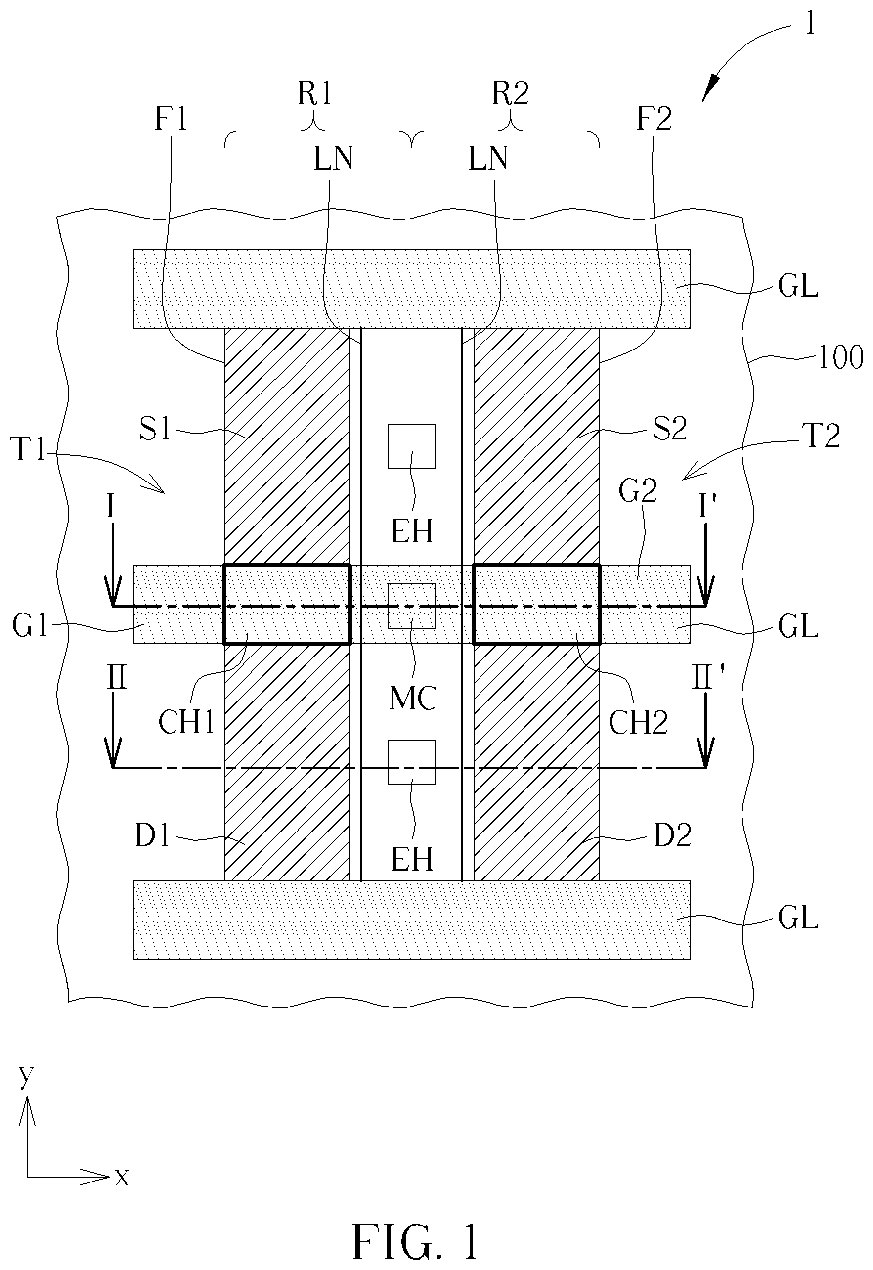
is a schematic layout diagram of a semiconductor transistor device according to an embodiment of the present invention. is a schematic cross-sectional view taken along line I-I′ in . is a schematic cross-sectional view taken along line II-IF in . to illustrate a method for fabricating a semiconductor transistor device according to an embodiment of the present invention, wherein and are schematic diagrams shown along line II-IF in , and are schematic diagrams of the layout of the semiconductor transistor device, and are schematic diagrams shown along line I-I′ and line II-IF in , respectively, and and are schematic diagrams shown along line I-I′ and line II-IF in , respectively.
DETAILED DESCRIPTION
In the following detailed description of the disclosure, reference is made to the accompanying drawings, which form a part hereof, and in which is shown, by way of illustration, specific embodiments in which the invention may be practiced. These embodiments are described in sufficient detail to enable those skilled in the art to practice the invention. Other embodiments may be utilized, and structural, logical, and electrical changes may be made without departing from the scope of the present invention. Therefore, the following detailed description is not to be considered as limiting, but the embodiments included herein are defined by the scope of the accompanying claims. Please refer to to 3 . is a schematic layout diagram of a semiconductor transistor device according to an embodiment of the present invention. is a schematic cross-sectional view taken along line I-I′ in . is a schematic cross-sectional view taken along line II-IF in . As shown in to 3 , the semiconductor transistor device 1 includes a substrate 100 , for example, a silicon substrate, having a first device region R 1 and a second device region R 2 adjacent to the first device region R 1 . According to an embodiment of the present invention, an isolation structure 110 is formed in the substrate 100 . According to an embodiment of the present invention, a first transistor T 1 is provided in the first device region R 1 , and a second transistor T 2 is provided in the second device region R 2 . According to an embodiment of the present invention, the first device region R 1 is, for example, an NMOS region, and the second device region R 2 is, for example, a PMOS region. According to an embodiment of the present invention, the first transistor T 1 is, for example, an NMOS transistor, and the second transistor T 2 is, for example, a PMOS transistor. According to an embodiment of the present invention, the first transistor T 1 includes a first fin structure F 1 on the substrate 100 , wherein the first fin structure F 1 includes a first source S 1 , a first drain D 1 , and a first channel CH 1 extending along a first direction (for example, the reference y-axis) between the first source S 1 and the first drain D 1 . According to an embodiment of the present invention, the first transistor T 1 further includes a gate G 1 extending along a second direction (for example, the reference x-axis), covering the first fin structure F 1 . According to an embodiment of the present invention, the second transistor T 2 includes a second fin structure F 2 on the substrate 100 , wherein the second fin structure T 2 includes a second source S 2 , a second drain D 2 , and a second channel CH 2 extending along the first direction (for example, the reference y-axis) between the second source S 2 and the second drain D 2 . According to an embodiment of the present invention, the second transistor T 2 further includes a gate G 2 extending along the second direction (for example, the reference x-axis), covering the second fin structure F 2 . According to an embodiment of the present invention, the gate G 1 and the gate G 2 may be metal gates. For example, the gate G 1 and the gate G 2 may comprise tungsten. As shown in , in regions other than the gate G 1 and the gate G 2 , the first transistor T 1 and the second transistor T 2 are covered by the first interlayer dielectric layer 210 . According to an embodiment of the present invention, the top surfaces of the gates G 1 and G 2 may be flush with the top surface of the first interlayer dielectric layer 210 . According to an embodiment of the present invention, the first transistor T 1 is spaced apart from the first transistor T 1 in the second direction (for example, the reference x-axis). According to an embodiment of the present invention, the first fin structure F 1 of the first transistor T 1 and the second fin structure F 2 of the second transistor T 2 are separated by an air gap AG, and the longitudinal axis of the air gap AG is parallel to the first direction (for example, the reference y-axis). According to an embodiment of the present invention, the air gap AG is disposed along a boundary (or a PN boundary) between the first device region R 1 and the second device region R 2 . According to an embodiment of the present invention, the extending direction of the air gap AG and the extending directions of the gate G 1 and the gate G 2 are perpendicular to each other. According to an embodiment of the present invention, as shown in and , the interior surface of the air gap AG is covered with a lining layer LN. According to an embodiment of the present invention, the lining layer LN may be, for example, a silicon oxide layer. According to an embodiment of the present invention, as shown in and , the first fin structure F 1 includes a first stack ST 1 of a plurality of nanosheets NS 1 , wherein each of the plurality of nanosheets NS 1 is surrounded by a first gate dielectric GD 1 . According to an embodiment of the invention, the second fin structure F 2 includes a second stack ST 2 of a plurality of nanosheets NS 2 , wherein each of the plurality of nanosheets NS 2 is surrounded by a second gate dielectric GD 2 . According to an embodiment of the present invention, the first gate dielectric GD 1 and the second gate dielectric GD 2 may be high-k dielectric materials such as hafnium oxide (HfO 2 ), but not limited thereto. According to an embodiment of the present invention, each of the plurality of nanosheets NS 1 , NS 2 may be formed of a channel material, for example, silicon. According to an embodiment of the present invention, a work function layer may be formed on the first gate dielectric GD 1 and the second gate dielectric GD 2 . For example, a P work function layer PWM may be formed on the second gate dielectric GD 2 in the second device region R 2 . An N work function layer NWM may be formed on the first gate dielectric GD 1 in the first device region R 1 and on the P work function layer PWM in the second device region R 2 . According to an embodiment of the present invention, the first interlayer dielectric layer 210 and the gates G 1 and G 2 are covered with a second interlayer dielectric layer 220 , and the second interlayer dielectric layer 220 is covered with a third interlayer dielectric layer 230 . According to an embodiment of the present invention, a first metal wiring pattern M 1 is formed in the third interlayer dielectric layer 230 . According to an embodiment of the present invention, metal contacts MC may be formed over the gate G 1 and the gate G 2 in the second interlayer dielectric layer 220 . According to an embodiment of the present invention, a contact hole EH is additionally provided above the air gap AG between two adjacent gate lines GL in the second interlayer dielectric layer 220 . According to an embodiment of the present invention, the upper end of the contact hole EH is sealed by the third interlayer dielectric layer 230 . According to an embodiment of the present invention, the air gap AG communicates with the sealed contact hole EH. The air gap AG can effectively reduce the parasitic capacitance and signal coupling between the first transistor T 1 and the second transistor T 2 , so as to improve the operation performance of the device. Please refer to to , which illustrate a method for fabricating a semiconductor transistor device according to an embodiment of the present invention, wherein to are schematic diagrams shown along line II-IF in . As shown in , a substrate 100 having a first device region R 1 and a second device region R 2 adjacent to the first device region R 1 is first provided. According to an embodiment of the present invention, an isolation structure 110 is formed in the substrate 100 . A first fin structure F 1 is formed in the first device region R 1 , and a second fin structure F 2 is formed in the second device region R 2 . According to an embodiment of the present invention, the first fin structure F 1 is composed of alternately laminated nanosheets NS 1 and SiGe epitaxial layers SS 1 , and the second fin structure F 2 is composed of alternately laminated nanosheets NS 2 and SiGe epitaxial layers SS 2 . According to embodiments of the present invention, the nanosheets NS 1 , NS 2 may be formed of a channel material, for example, silicon. A trench 200 with a width w of about 5-20 nanometers is formed at the boundary between the first device region R 1 and the second device region R 2 . As shown in , subsequently, a lining layer LN and a sacrificial layer SAC are deposited in a blanket manner by a chemical vapor deposition (CVD) process in the first device region R 1 and the second device region R 2 on the substrate 100 . According to an embodiment of the present invention, the lining layer LN may be, for example, a silicon oxide layer. According to an embodiment of the present invention, the sacrificial layer SAC may be, for example, a silicon nitride layer. At this point, the trench 200 between the first device region R 1 and the second device region R 2 is filled with the lining layer LN and the sacrificial layer SAC. As shown in , next, an anisotropic dry etching process is performed to etch the sacrificial layer SAC on the lining layer LN. According to an embodiment of the present invention, the sacrificial layer SAC filled in the trench 200 between the first device region R 1 and the second device region R 2 is not removed. As shown in , a dummy silicon oxide layer DOL is conformally deposited on the lining layer LN and the sacrificial layer SAC in the first and second device regions R 1 and R 2 . A dummy gate layer DGL is then deposited on the dummy silicon oxide layer DOL. According to an embodiment of the present invention, for example, the dummy gate layer DGL may be a polysilicon layer or an amorphous silicon layer. Subsequent process steps for making transistors can be performed, including, but not limited to, gate patterning, formation of inner spacers, etching of sacrificial layer SAC, epitaxy of source and drain, first interlayer dielectric layer deposition, planarization process, and replacement metal gate (RMG) process. The above steps are all well-known processes, and will not be described in detail. As shown in to , the first transistor T 1 is formed in the first device region R 1 , and the second transistor T 2 is formed in the second device region R 2 . According to an embodiment of the present invention, the first device region R 1 is, for example, an NMOS region, and the second device region R 2 is, for example, a PMOS region. According to an embodiment of the present invention, the first transistor T 1 is, for example, an NMOS transistor, and the second transistor T 2 is, for example, a PMOS transistor. According to an embodiment of the present invention, the first transistor T 1 includes a first fin structure F 1 on the substrate 100 , wherein the first fin structure F 1 includes a first source S 1 , a first drain D 1 , and a first channel CH 1 extending along the first direction (for example, reference y-axis) between the first source S 1 and the first drain D 1 . According to an embodiment of the present invention, the first transistor T 1 further includes a gate G 1 extending along the second direction (for example, the reference x-axis), covering the first fin structure F 1 . According to an embodiment of the present invention, the second transistor T 2 includes a second fin structure F 2 on the substrate 100 , wherein the second fin structure T 2 includes a second source S 2 , a second drain D 2 , and a second channel CH 2 extending along the first direction (for example, the reference y-axis) between the second source S 2 and the second drain D 2 . According to an embodiment of the present invention, the second transistor T 2 further includes a gate G 2 extending along the second direction (for example, the reference x-axis), covering the second fin structure F 2 . According to an embodiment of the present invention, the gate G 1 and the gate G 2 may be metal gates. According to an embodiment of the present invention, a work function layer may be formed on the first gate dielectric GD 1 and the second gate dielectric GD 2 . For example, a P work function layer PWM may be formed on the second gate dielectric GD 2 in the second device region R 2 . An N work function layer NWM may be formed on the first gate dielectric GD 1 in the first device region R 1 and on the P work function layer PWM in the second device region R 2 . At this point, the sacrificial layer SAC and the lining layer LN constitute a temporary dielectric wall DW between the first transistor T 1 and the second transistor T 2 . As shown in to , after the fabrication of the first transistor T 1 and the second transistor T 2 is completed, a second interlayer dielectric layer 220 is deposited in the first device region R 1 and the second device region R 2 , so that the second interlayer dielectric layer 220 covers the first interlayer dielectric layer 210 , the gate G 1 and the gate G 2 . According to an embodiment of the present invention, next, metal contacts MC are formed on the gate G 1 and the gate G 2 in the second interlayer dielectric layer 220 . A contact hole EH is formed above the temporary dielectric wall DW between two adjacent gate lines GL in the second interlayer dielectric layer 220 , so that the contact hole EH exposes a part of the top surface of the temporary dielectric wall DW. As shown in , a wet etching process is then performed and the temporary dielectric wall DW is removed through the contact hole EH, thereby forming an air gap AG between the first fin structure F 1 and the second fin structure F 2 . The first fin structure F 1 and the second fin structures F 2 are separated from each other by the air gaps AG. Finally, as shown in , a third interlayer dielectric layer 230 is deposited on the second interlayer dielectric layer 220 . According to an embodiment of the present invention, a first metal wiring pattern M 1 may be formed in the third interlayer dielectric layer 230 . According to an embodiment of the present invention, the upper end of the contact hole EH is sealed by the third interlayer dielectric layer 230 . According to an embodiment of the present invention, the air gap AG communicates with the sealed contact hole EH. The air gap AG can effectively reduce the parasitic capacitance and signal coupling between the first transistor T 1 and the second transistor T 2 , so as to improve the operation performance of the device. Those skilled in the art will readily observe that numerous modifications and alterations of the device and method may be made while retaining the teachings of the invention. Accordingly, the above disclosure should be construed as limited only by the metes and bounds of the appended claims.
Figures (9)
Citations
This patent cites (4)
- US9997463
- US10714585
- US11164942
- US2023/0178559