Driving Circuit for Driving Either Voltage-driven or Current-driven Switch
Abstract
An electronic circuit includes a driving circuit and a power switch. The driving circuit includes a first control circuit and a second control circuit. The first control circuit is coupled between a high-level voltage and an internal node. The second control circuit includes a first switch and a second switch. The first switch is coupled between the internal node and a driving node, and the second switch is coupled between the driving node and a first low-level voltage. The second control circuit periodically couples the first control circuit and the first low-level voltage to a driving node. The power switch is coupled to a second low-level voltage and turned on or off in response to a driving signal at the driving node. The power switch is either current-driven or voltage-driven.
Claims (30)
1 . An electronic circuit, comprising: a driving circuit, comprising: a first control circuit, coupled between a high-level voltage and an internal node; and a second control circuit, comprising a first switch and a second switch, wherein the first switch is coupled between the internal node and a driving node, and the second switch is coupled between the driving node and a first low-level voltage, wherein the second control circuit periodically couples the first control circuit and the first low-level voltage to the driving node; and a power switch, coupled to a second low-level voltage and turned on or off in response to a driving signal at the driving node; wherein the power switch is either current-driven or voltage-driven; wherein the first control circuit comprises: a current source, coupled between the high-level voltage and the internal node and generating a fixed current; wherein the current source comprises: a first resistor, coupled between the high-level voltage and a first node and generating a first current; a reference generator, generating a reference voltage at a second node based on the first current; a second resistor, coupled between the second node and the internal node and generating a second current with the reference voltage; and an NPN transistor, comprising a collector, a base, and an emitter, wherein the collector is coupled to the high-level voltage, the base is coupled to the first node, and the emitter is coupled to the second node; wherein the fixed current is equal to a sum of the first current and the second current.
4 . An electronic circuit, comprising: a driving circuit, comprising: a first control circuit, coupled between a high-level voltage and an internal node; and a second control circuit, comprising a first switch and a second switch, wherein the first switch is coupled between the internal node and a driving node, and the second switch is coupled between the driving node and a first low-level voltage, wherein the second control circuit periodically couples the first control circuit and the first low-level voltage to a driving node; and a power switch, coupled to a second low-level voltage and turned on or off in response to a driving signal at the driving node; wherein the power switch is either current-driven or voltage-driven; wherein the first control circuit comprises: a current source, coupled between the high-level voltage and the internal node and generating a fixed current; wherein the current source comprises: a normally-on transistor, comprising a drain terminal, a gate terminal, and a source terminal, wherein the drain terminal is coupled to the high-level voltage and the gate terminal is coupled to the internal node; and a first resistor, coupled between the source terminal and the internal node; wherein the fixed current is generated based on the first resistor and a voltage across the source terminal and the gate terminal.
6 . An electronic circuit, comprising: a driving circuit, comprising: a first control circuit, coupled between a high-level voltage and an internal node; and a second control circuit, comprising a first switch and a second switch, wherein the first switch is coupled between the internal node and a driving node, and the second switch is coupled between the driving node and a first low-level voltage, wherein the second control circuit periodically couples the first control circuit and the first low-level voltage to a driving node; and a power switch, coupled to a second low-level voltage and turned on or off in response to a driving signal at the driving node; wherein the power switch is either current-driven or voltage-driven; wherein the first control circuit comprises: a current source, coupled between the high-level voltage and the internal node and generating a fixed current; wherein the first control circuit further comprises: a diode, comprising an anode and a cathode, wherein the anode is coupled to the internal node and the cathode is coupled to the high-level voltage.
Show 27 dependent claims
2 . The electronic circuit as defined in claim 1 , wherein the first low-level voltage is equal to the second low-level voltage.
3 . The electronic circuit as defined in claim 1 , wherein the first low-level voltage is not equal to the second low-level voltage.
5 . The electronic circuit as defined in claim 1 , wherein the first control circuit further comprises: a capacitor, coupled between the high-level voltage and the internal node.
7 . The electronic circuit as defined in claim 1 , wherein the driving circuit further comprises: a dividing circuit, comprising: a first dividing resistor, coupled between the high-level voltage and the internal node; and a second dividing resistor, coupled between the driving node and the second low-level voltage; wherein the dividing circuit is configured to determine a voltage of the driving node.
8 . The electronic circuit as defined in claim 1 , wherein the driving circuit further comprises: a voltage clamp unit, coupled between the driving node and the second low-level voltage; wherein the voltage clamp unit is configured to clamp a voltage between the driving node and the second low-level voltage.
9 . The electronic circuit as defined in claim 8 , wherein the voltage clamp unit comprises: a Zener diode, comprising a anode and a cathode; wherein the anode is coupled to the second low-level voltage, and the cathode is coupled to the driving node.
10 . The electronic circuit as defined in claim 8 , wherein the voltage clamp unit comprises: a Zener diode, comprising a anode and a cathode; wherein the anode is coupled to the driving node, and the cathode is coupled to the second low-level voltage.
11 . The electronic circuit as defined in claim 8 , wherein the voltage clamp unit comprises: a first Zener diode, comprising a first anode and a first cathode; and a second Zener diode, comprising a second anode and a second cathode; wherein the first anode is coupled to the second anode; wherein the first cathode is coupled to the driving node; wherein the second cathode is coupled to the second low-level voltage.
12 . The electronic circuit as defined in claim 8 , wherein the voltage clamp unit comprises: a diode, comprising a first anode and a first cathode; and a Zener diode, comprising a second anode and a second cathode; wherein the first anode is coupled to the driving node; wherein the first cathode is coupled to the second cathode; wherein the second anode is coupled to the second low-level voltage.
13 . The electronic circuit as defined in claim 8 , wherein the voltage clamp unit comprises: a Zener diode, comprising a first anode and a first cathode; and a diode, comprising a second anode and a second cathode; wherein the first anode is coupled to the driving node; wherein the first cathode is coupled to the second cathode; wherein the second anode is coupled to the second low-level voltage.
14 . The electronic circuit as defined in claim 8 , wherein the voltage clamp unit comprises: a first diode, comprising a first anode and a first cathode; a second diode, comprising a second anode and a second cathode; and a third diode, comprising a third anode and a third cathode; wherein the first anode is coupled to the driving node; wherein the first cathode is coupled to the second anode; wherein the second cathode is coupled to the second low-level voltage; wherein the third anode is coupled to the second low-level voltage; wherein the third cathode is coupled to the driving node.
15 . The electronic circuit as defined in claim 8 , wherein the voltage clamp unit comprises: a first diode, comprising a first anode and a first cathode; wherein the first anode is coupled to the second low-level voltage; wherein the first cathode is coupled to the driving node.
16 . The electronic circuit as defined in claim 8 , wherein the voltage clamp unit comprises: a first diode, comprising a first anode and a first cathode; wherein the first anode is coupled to the driving node; wherein the first cathode is coupled to the second low-level voltage.
17 . The electronic circuit as defined in claim 8 , wherein the voltage clamp unit comprises: a first diode, comprising a first anode and a first cathode; and a second diode, comprising a second anode and a second cathode; wherein the first anode is coupled to the second low-level voltage; wherein the first cathode is coupled to the driving node; wherein the second anode is coupled to the driving node; wherein the second cathode is coupled to the second low-level voltage.
18 . The electronic circuit as defined in claim 8 , wherein the voltage clamp unit comprises: a first N-type transistor, comprising a first drain terminal, a first gate terminal, a first source terminal, and a first base terminal; a second N-type transistor, comprising a second drain terminal, a second gate terminal, a second source terminal, and a second base terminal; and a third N-type transistor, comprising a third drain terminal, a third gate terminal, a third source terminal, and a third base terminal; wherein the first source terminal is coupled to the first gate terminal, the first base terminal, the driving node, and the third drain terminal; wherein the first drain terminal is coupled to the second source terminal, the second gate terminal, and the second base terminal; wherein the second drain terminal is coupled to the second low-level voltage, the third source terminal, the third gate terminal, and the third base terminal.
19 . The electronic circuit as defined in claim 8 , wherein the voltage clamp unit comprises: a first N-type transistor, comprising a first drain terminal, a first gate terminal, a first source terminal, and a first base terminal; wherein the first source terminal is coupled to the first gate terminal, the first base terminal, and the second low-level voltage; wherein the first drain terminal is coupled to the driving node.
20 . The electronic circuit as defined in claim 8 , wherein the voltage clamp unit comprises: a first N-type transistor, comprising a first drain terminal, a first gate terminal, a first source terminal, and a first base terminal; wherein the first source terminal is coupled to the first gate terminal, the first base terminal, and the driving node; wherein the first drain terminal is coupled to the second low-level voltage.
21 . The electronic circuit as defined in claim 8 , wherein the driving circuit further comprises: a voltage-controlled switch, comprising a first terminal, a second terminal, and a control terminal; wherein the first terminal is coupled to the driving node; wherein the second terminal is coupled to a gate terminal of the power switch; wherein the voltage clamp unit is coupled between the control node and the second low-level voltage.
22 . The electronic circuit as defined in claim 21 , wherein when the first switch is turned on, the high-level voltage is provided to the control terminal of the voltage-controlled switch through a parasitic capacitance between the first terminal and the control terminal; wherein the voltage-controlled switch is turned on or off in response to a voltage of the control terminal.
23 . The electronic circuit as defined in claim 21 , wherein the voltage-controlled switch comprises: a normally-on transistor, comprising the first terminal, the second terminal, and the control terminal; wherein when a voltage of the control terminal to the second terminal is less than a threshold of the normally-on transistor, the normally-on transistor is turned off so as to set a voltage of the gate terminal of the power switch; wherein a voltage of the control terminal is determined by the voltage clamp unit.
24 . The electronic circuit as defined in claim 21 , wherein the voltage-controlled switch comprises: a normally-off transistor, comprising the first terminal, the second terminal, and the control terminal; wherein when a voltage of the control terminal to the second terminal is less than a threshold of the normally-off transistor, the normally-off transistor is turned off so as to set a voltage of the gate terminal of the power switch; wherein a voltage of the control terminal is determined by the voltage clamp unit.
25 . The electronic circuit as defined in claim 21 , wherein the voltage-controlled switch comprises: an NPN transistor, comprising a collector, a base, and an emitter; wherein the collector corresponds to the first terminal, the base corresponds to the control terminal, and the emitter corresponds to the second terminal; wherein when a voltage of the base to the emitter is less than a cut-off voltage of the NPN transistor, the NPN transistor is turned off so as to set a voltage of the gate terminal of the power switch; wherein a voltage of the control terminal is determined by the voltage clamp unit.
26 . The electronic circuit as defined in claim 21 , wherein the voltage-controlled circuit comprises: a feedthrough resistor, coupled between the gate terminal of the power switch and the control terminal.
27 . The electronic circuit as defined in claim 26 , wherein a voltage of the gate terminal of the power switch is equal to a sum of a voltage across the feedthrough resistor and a voltage of the control terminal.
28 . The electronic circuit as defined in claim 8 , wherein the driving circuit further comprises: a damping circuit, coupled between the driving node and a gate terminal of the power switch; wherein the damping circuit is configured to prevent oscillation at the gate terminal of the power switch.
29 . The electronic circuit as defined in claim 28 , wherein the damping circuit comprises: a first damping resistor, coupled between the driving node and the gate terminal of the power switch; and a diode, comprising an anode and a cathode, wherein the anode is coupled to the gate terminal of the power switch and the cathode is coupled to the driving node.
30 . The electronic circuit as defined in claim 29 , wherein the damping circuit comprises: a second damping resistor, coupled between the cathode and the driving node.
Full Description
Show full text →
CROSS REFERENCE TO RELATED APPLICATIONS
This application claims the benefit of U.S. Provisional Application No. 63/439,988, filed on Jan. 19, 2023, the entirety of which is incorporated by reference herein.
BACKGROUND OF THE INVENTION
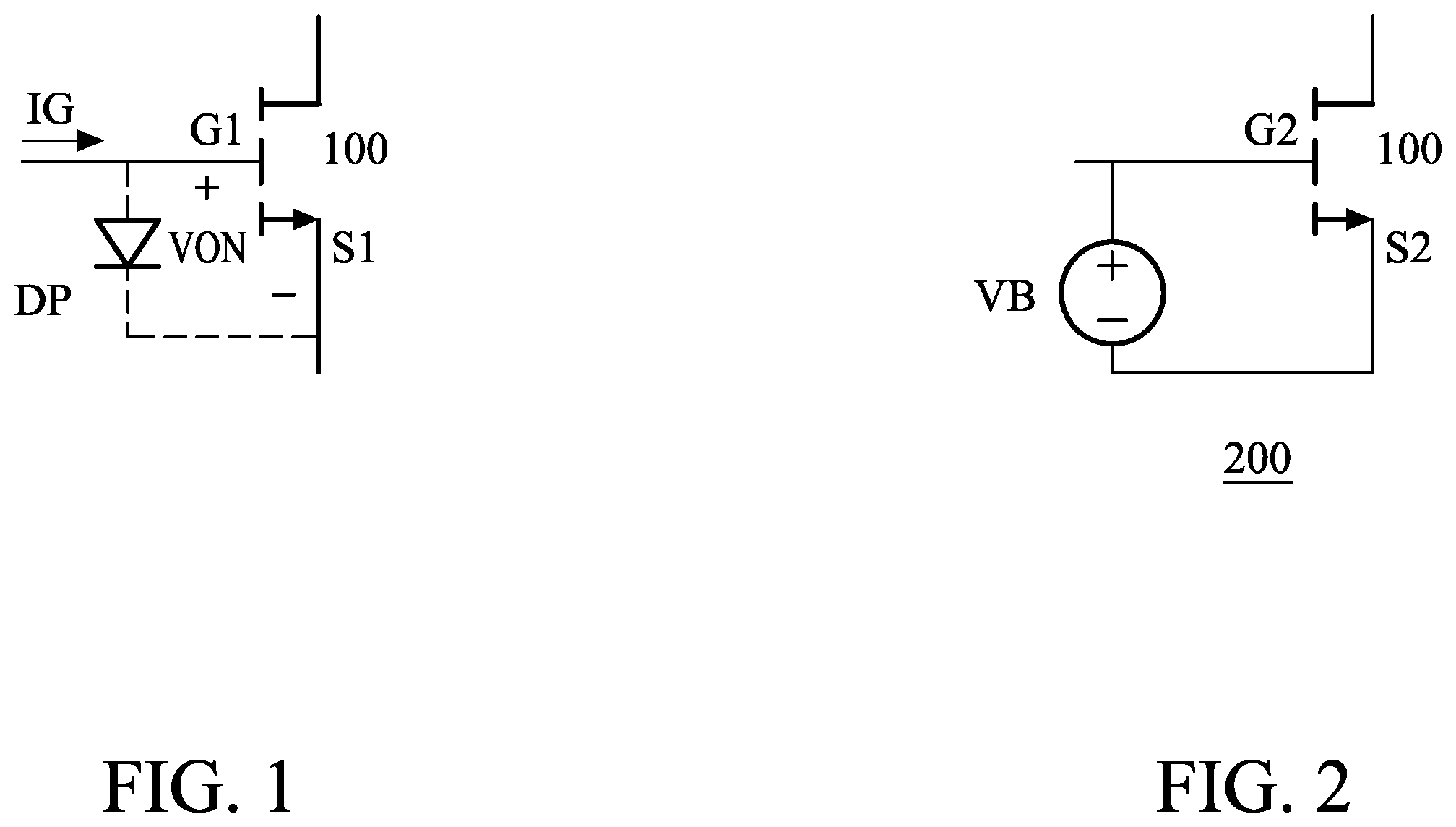
Field of the Invention The disclosure is generally related to driving circuit that is able to drive either a voltage-driven or a current-driven switch. Description of the Related Art With the development of technology, many types of switches have been developed. Those transistors may be divided into two categories: current-driven switches and voltage-driven switches. Since current-driven switches and voltage-driven switches are driven by current and voltage, respectively, it is difficult to drive these two types of switches with an identical driving circuit. illustrates a schematic diagram of a current-driven transistor. As shown in , the current-driven transistor 100 includes a parasitic diode DP, where the parasitic diode DP is coupled between the first gate terminal G 1 and the first source terminal S 1 of the current-driven transistor 100 . When the current-driven transistor 100 is turned on, a gate current IG is required to forward-biased the parasitic diode DP to generate a turn-on voltage VON across the first gate terminal G 1 to the first source terminal S 1 . illustrates a schematic diagram of a voltage-driven transistor. As shown in , when the voltage-driven transistor 200 is turned on, a bias voltage VB is applied across the second gate terminal G 2 and the second source terminal S 2 of the voltage-driven transistor 200 . Comparing the current-driven transistor 100 and the voltage-driven transistor 200 , the current-driven transistor 100 needs the gate current IG and the turn-on voltage VON to be turned on, while the voltage-driven transistor 200 only needs the bias voltage VB to be turned on. With the increasing popularity of switching circuits, driving circuits for driving switches become more significant. Once a driving circuit for driving both a current-driven switch and a voltage-driven switch is proposed, it would be really convenient for engineers to freely utilize a current-driven switch or a voltage-driven switch in their designs. BRIEF
SUMMARY OF THE INVENTION
Driving circuits that are able to drive a current-driven switch and a voltage-driven switch are proposed herein. The proposed driving circuits are able to set the proper voltage at the gate terminal to keep the voltage-driven switch on, and they also provide a fixed current to keep the current-driven switch on. It makes it more convenient for engineers to be able to freely utilize a current-driven switch or a voltage-driven switch in their designs. In an embodiment, an electronic circuit is proposed, which comprises a driving circuit and a power switch. The driving circuit comprises a first control circuit and a second control circuit. The first control circuit is coupled between a high-level voltage and an internal node. The second control circuit comprises a first switch and a second switch, wherein the first switch is coupled between the internal node and a driving node, and the second switch is coupled between the driving node and a first low-level voltage. The second control circuit periodically couples the first control circuit and the first low-level voltage to a driving node. The power switch is coupled to a second low-level voltage and turned on or off in response to a driving signal at the driving node. The power switch is either current-driven or voltage-driven. According to an embodiment of the preset disclosure, the first low-level voltage is equal to the second low-level voltage. According to another embodiment of the preset disclosure, the first low-level voltage is not equal to the second low-level voltage. According to an embodiment of the preset disclosure, the first control circuit comprises a current source. The current source is coupled between the high-level voltage and the internal node and generating a fixed current. According to an embodiment of the preset disclosure, the current source comprises a first resistor, a reference generator, a second resistor, and an NPN transistor. The first resistor is coupled between the high-level voltage and a first node and generates first current. The reference generator generates a reference voltage at a second node based on the first current. The second resistor is coupled between the second node and the internal node and generates a second current with the reference voltage. The NPN transistor comprises a collector, a base, and an emitter, where the collector is coupled to the high-level voltage, the base is coupled to the first node, and the emitter is coupled to the second node. The fixed current is equal to a sum of the first current and the second current. According to another embodiment of the preset disclosure, the current source comprises a normally-on transistor and a first resistor. The normally-on transistor comprises a drain terminal, a gate terminal, and a source terminal, where the drain terminal is coupled to the high-level voltage and the gate terminal is coupled to the internal node. The first resistor is coupled between the source terminal and the internal node. The fixed current is generated based on the first resistor and a voltage across the source terminal and the gate terminal. According to an embodiment of the preset disclosure, the first control circuit further comprises a capacitor. The capacitor is coupled between the high-level voltage and the internal node. According to another embodiment of the preset disclosure, the first control circuit further comprises a diode. The diode comprises an anode and a cathode, where the anode is coupled to the internal node and the cathode is coupled to the high-level voltage. According to an embodiment of the preset disclosure, the driving circuit further comprises a dividing circuit comprising a first dividing resistor and a second dividing resistor. The first dividing resistor is coupled between the high-level voltage and the internal node. The second dividing resistor is coupled between the driving node and the second low-level voltage. The dividing circuit is configured to determine a voltage of the driving node. According to an embodiment of the preset disclosure, the driving circuit further comprises a voltage clamp unit. The voltage clamp unit is coupled between the driving node and the second low-level voltage. The voltage clamp unit is configured to clamp a voltage between the driving node and the second low-level voltage. According to an embodiment of the preset disclosure, the voltage clamp unit comprises a Zener diode. The Zener diode comprises a anode and a cathode. The anode is coupled to the second low-level voltage, and the cathode is coupled to the driving node. According to another embodiment of the preset disclosure, the voltage clamp unit comprises a Zener diode comprising a anode and a cathode. The anode is coupled to the driving node, and the cathode is coupled to the second low-level voltage. According to yet another embodiment of the preset disclosure, the voltage clamp unit comprises a first Zener diode comprising a first anode and a first cathode and a second Zener diode comprising a second anode and a second cathode. The first anode is coupled to the second anode. The first cathode is coupled to the driving node. The second cathode is coupled to the second low-level voltage. According to yet another embodiment of the preset disclosure, the voltage clamp unit comprises a diode comprising a first anode and a first cathode and a Zener diode comprising a second anode and a second cathode. The first anode is coupled to the driving node. The first cathode is coupled to the second cathode. The second anode is coupled to the second low-level voltage. According to yet another embodiment of the preset disclosure, the voltage clamp unit comprises a Zener diode comprising a first anode and a first cathode and a diode comprising a second anode and a second cathode. The first anode is coupled to the driving node. The first cathode is coupled to the second cathode. The second anode is coupled to the second low-level voltage. According to yet another embodiment of the preset disclosure, the voltage clamp unit comprises a first diode comprising a first anode and a first cathode and a second diode comprising a second anode and a second cathode. The first anode is coupled to the driving node. The first cathode is coupled to the second anode. The second cathode is coupled to the second low-level voltage. According to yet another embodiment of the preset disclosure, the voltage clamp unit comprises a first diode comprising a first anode and a first cathode, a second diode, comprising a second anode and a second cathode, and a third diode comprising a third anode and a third cathode. The first anode is coupled to the driving node. The first cathode is coupled to the second anode. The second cathode is coupled to the second low-level voltage. The third anode is coupled to the second low-level voltage. The third cathode is coupled to the driving node. According to yet another embodiment of the preset disclosure, the voltage clamp unit comprises a first diode comprising a first anode and a first cathode. The first anode is coupled to the second low-level voltage. The first cathode is coupled to the driving node. According to yet another embodiment of the preset disclosure, the voltage clamp unit comprises a first diode comprising a first anode and a first cathode. The first anode is coupled to the driving node. The first cathode is coupled to the second low-level voltage. According to yet another embodiment of the preset disclosure, the voltage clamp unit comprises a first diode comprising a first anode and a first cathode and a second diode comprising a second anode and a second cathode. The first anode is coupled to the second low-level voltage. The first cathode is coupled to the driving node. The second anode is coupled to the driving node. The second cathode is coupled to the second low-level voltage. According to yet another embodiment of the preset disclosure, the voltage clamp unit comprises a first N-type transistor comprising a first drain terminal, a first gate terminal, a first source terminal, and a first base terminal and a second N-type transistor comprising a second drain terminal, a second gate terminal, a second source terminal, and a second base terminal. The first source terminal is coupled to the first gate terminal, the first base terminal, and the driving node. The first drain terminal is coupled to the second source terminal, the second gate terminal, and the second base terminal. The second drain terminal is coupled to the second low-level voltage. According to yet another embodiment of the preset disclosure, the voltage clamp unit comprises a first N-type transistor comprising a first drain terminal, a first gate terminal, a first source terminal, and a first base terminal, a second N-type transistor comprising a second drain terminal, a second gate terminal, a second source terminal, and a second base terminal, and a third N-type transistor comprising a third drain terminal, a third gate terminal, a third source terminal, and a third base terminal. The first source terminal is coupled to the first gate terminal, the first base terminal, the driving node, and the third drain terminal. The first drain terminal is coupled to the second source terminal, the second gate terminal, and the second base terminal. The second drain terminal is coupled to the second low-level voltage, the third source terminal, the third gate terminal, and the third base terminal. According to yet another embodiment of the preset disclosure, the voltage clamp unit comprises a first N-type transistor comprising a first drain terminal, a first gate terminal, a first source terminal, and a first base terminal. The first source terminal is coupled to the first gate terminal, the first base terminal, and the second low-level voltage. The first drain terminal is coupled to the driving node. According to yet another embodiment of the preset disclosure, the voltage clamp unit comprises a first N-type transistor comprising a first drain terminal, a first gate terminal, a first source terminal, and a first base terminal. The first source terminal is coupled to the first gate terminal, the first base terminal, and the driving node. The first drain terminal is coupled to the second low-level voltage. According to another embodiment of the preset disclosure, the driving circuit further comprises a voltage-controlled switch comprising a first terminal, a second terminal, and a control terminal. The first terminal is coupled to the driving node. The second terminal is coupled to a gate terminal of the power switch. The voltage clamp unit is coupled between the control node and the second low-level voltage. According to an embodiment of the preset disclosure, when the first switch is turned on, the high-level voltage is provided to the control terminal of the voltage-controlled switch through a parasitic capacitance between the first terminal and the control terminal. The voltage-controlled switch is turned on or off in response to a voltage of the control terminal. According to an embodiment of the preset disclosure, the voltage-controlled switch comprises a normally-on transistor comprising the first terminal, the second terminal, and the control terminal. When a voltage of the control terminal to the second terminal is less than a threshold of the normally-on transistor, the normally-on transistor is turned off so as to set a voltage of the gate terminal of the power switch. A voltage of the control terminal is determined by the voltage clamp unit. According to another embodiment of the preset disclosure, the voltage-controlled switch comprises a normally-off transistor comprising the first terminal, the second terminal, and the control terminal. When a voltage of the control terminal to the second terminal is less than a threshold of the normally-off transistor, the normally-off transistor is turned off so as to set a voltage of the gate terminal of the power switch. A voltage of the control terminal is determined by the voltage clamp unit. According to yet another embodiment of the preset disclosure, the voltage-controlled switch comprises an NPN transistor comprising a collector, a base, and an emitter. The collector corresponds to the first terminal, the base corresponds to the control terminal, and the emitter corresponds to the second terminal. When a voltage of the base to the emitter is less than a cut-off voltage of the NPN transistor, the NPN transistor is turned off so as to set a voltage of the gate terminal of the power switch. A voltage of the control terminal is determined by the voltage clamp unit. According to yet another embodiment of the preset disclosure, the voltage-controlled circuit comprises a feedthrough resistor. The feedthrough resistor is coupled between the gate terminal of the power switch and the control terminal. According to an embodiment of the preset disclosure, a voltage of the gate terminal of the power switch is equal to a sum of a voltage across the feedthrough resistor and a voltage of the control terminal. According to yet another embodiment of the preset disclosure, the driving circuit further comprises a damping circuit. The damping circuit is coupled between the driving node and a gate terminal of the power switch. The damping circuit is configured to prevent oscillation at the gate terminal of the power switch. According to an embodiment of the preset disclosure, the damping circuit comprises a first damping resistor and a diode. The first damping resistor is coupled between the driving node and the gate terminal of the power switch. The diode comprises an anode and a cathode. The anode is coupled to the gate terminal of the power switch and the cathode is coupled to the driving node. According to another embodiment of the preset disclosure, the damping circuit comprises a second damping resistor. The second damping resistor is coupled between the cathode and the driving node. A detailed description is given in the following embodiments with reference to the accompanying drawings.
BRIEF DESCRIPTION OF DRAWINGS
The invention can be more fully understood by reading the subsequent detailed description and examples with references made to the accompanying drawings, wherein: illustrates a schematic diagram of a current-driven transistor; illustrates a schematic diagram of a voltage-driven transistor; is a block diagram of an electronic circuit in accordance with an embodiment of the present disclosure; is a schematic diagram of a current source in accordance with an embodiment of the present disclosure; is a schematic diagram of a current source in accordance with another embodiment of the present disclosure; is a schematic diagram of a first control circuit in accordance with another embodiment of the present disclosure; is a schematic diagram of a first control circuit in accordance with yet another embodiment of the present disclosure; is a schematic diagram of an electronic circuit in accordance with another embodiment of the present disclosure; is a schematic diagram of an electronic circuit in accordance with yet another embodiment of the present disclosure; a schematic diagram of a voltage clamp unit in accordance with an embodiment of the present disclosure; is a schematic diagram of a voltage clamp unit in accordance with another embodiment of the present disclosure; is a schematic diagram of a voltage clamp unit in accordance with yet another embodiment of the present disclosure; is a schematic diagram of a voltage clamp unit in accordance with yet another embodiment of the present disclosure; is a schematic diagram of a voltage clamp unit in accordance with yet another embodiment of the present disclosure; is a schematic diagram of a voltage clamp unit in accordance with yet another embodiment of the present disclosure; is a schematic diagram of a voltage clamp unit in accordance with yet another embodiment of the present disclosure; is a schematic diagram of a voltage clamp unit in accordance with yet another embodiment of the present disclosure; is a schematic diagram of a voltage clamp unit in accordance with yet another embodiment of the present disclosure; is a schematic diagram of a voltage clamp unit in accordance with yet another embodiment of the present disclosure; is a schematic diagram of a voltage clamp unit in accordance with yet another embodiment of the present disclosure; is a schematic diagram of a voltage clamp unit in accordance with yet another embodiment of the present disclosure; is a schematic diagram of a voltage clamp unit in accordance with yet another embodiment of the present disclosure; is a schematic diagram of a voltage clamp unit in accordance with yet another embodiment of the present disclosure; is a schematic diagram of an electronic circuit in accordance with yet another embodiment of the present disclosure; is a schematic diagram of a voltage-controlled switch in accordance with an embodiment of the present disclosure; is a schematic diagram of a voltage-controlled switch in accordance with another embodiment of the present disclosure; is a schematic diagram of a voltage-controlled switch in accordance with yet another embodiment of the present disclosure; is a schematic diagram of an electronic circuit in accordance with yet another embodiment of the present disclosure; is a schematic diagram of an electronic circuit in accordance with yet another embodiment of the present disclosure; is a schematic diagram of an electronic circuit in accordance with yet another embodiment of the present disclosure; and is a schematic diagram of an electronic circuit in accordance with yet another embodiment of the present disclosure.
DETAILED DESCRIPTION
OF THE INVENTION The following description is made for the purpose of illustrating the general principles of the disclosure and should not be taken in a limiting sense. The scope of the disclosure is determined by reference to the appended claims. In the following detailed description, for purposes of explanation, numerous specific details and embodiments are set forth in order to provide a thorough understanding of the present disclosure. The use of like and/or corresponding numerals in the drawings of different embodiments does not suggest any correlation between different embodiments. In addition, in some embodiments of the present disclosure, terms concerning attachments, coupling and the like, such as “connected” and “interconnected,” refer to a relationship wherein structures are secured or attached to one another either directly or indirectly (for example, electrically connection) via intervening structures, as well as both movable or rigid attachments or relationships, unless expressly described otherwise. In addition, in this specification, relative spatial expressions are used. For example, “lower”, “bottom”, “higher” or “top” are used to describe the position of one element relative to another. It should be appreciated that if a device is flipped upside down, an element that is “lower” will become an element that is “higher”. It should be understood that, although the terms first, second, third etc. may be used herein to describe various elements, components, regions, layers, portions and/or sections, these elements, components, regions, layers, portions and/or sections should not be limited by these terms. These terms are only used to distinguish one element, component, region, layer, portion or section from another element, component, region, layer or section. Thus, a first element, component, region, layer, portion or section in the specification could be termed a second element, component, region, layer, portion or section in the claims without departing from the teachings of the present disclosure. It should be understood that this description of the exemplary embodiments is intended to be read in connection with the accompanying drawings, which are to be considered part of the entire written description. The drawings are not drawn to scale. In addition, structures and devices are shown schematically in order to simplify the drawing. The terms “approximately”, “about” and “substantially” typically mean a value is within a range of +/−20% of the stated value, more typically a range of +/−10%, +/−5%, +/−3%, +/−2%, +/−1% or +/−0.5% of the stated value. The stated value of the present disclosure is an approximate value. Even there is no specific description, the stated value still includes the meaning of “approximately”, “about” or “substantially”. Unless defined otherwise, all technical and scientific terms used herein have the same meaning as commonly understood by one of ordinary skill in the art to which this disclosure belongs. It should be appreciated that, in each case, the term, which is defined in a commonly used dictionary, should be interpreted as having a meaning that conforms to the relative skills of the present disclosure and the background or the context of the present disclosure, and should not be interpreted in an idealized or overly formal manner unless so defined. In addition, in some embodiments of the present disclosure, terms concerning attachments, coupling and the like, such as “connected” and “interconnected,” refer to a relationship wherein structures are secured or attached to one another either directly or indirectly (for example, electrically connection) via intervening structures, as well as both movable or rigid attachments or relationships, unless expressly described otherwise. In the drawings, similar elements and/or features may have the same reference number. Various components of the same type can be distinguished by adding letters or numbers after the component symbol to distinguish similar components and/or similar features. In addition, in some embodiments of the present disclosure, terms concerning attachments, coupling and the like, such as “connected” and “interconnected,” refer to a relationship wherein structures are secured or attached to one another either directly or indirectly (for example, electrically connection) via intervening structures, as well as both movable or rigid attachments or relationships, unless expressly described otherwise. is a block diagram of an electronic circuit in accordance with an embodiment of the present disclosure. As shown in , the electronic circuit 300 includes a driving circuit 310 and a power switch 320 . The driving circuit 310 includes a first control circuit 311 and a second control circuit 312 . The first control circuit 311 is coupled between the high-level voltage VH and an internal node NI and includes a current source CS. The second control circuit 312 includes a first switch S 1 and a second switch S 2 . The first switch S 1 is coupled between the internal node NI and a driving node ND. The second switch S 2 is coupled between the driving node ND and a first low-level voltage VL 1 . The power switch 320 includes a third gate terminal G 3 , a third source terminal S 3 , and a third drain terminal D 3 . The third gate terminal G 3 is coupled to the driving node ND, and the third source terminal S 3 is coupled to a second low-level voltage VL 2 . The third drain terminal D 3 receives operating voltage and current from other circuits. According to some embodiments of the present disclosure, the first low-level voltage VL 1 may be identical to the second low-level voltage VL 2 . According to other embodiments of the present disclosure, the first low-level voltage VL 1 may be different from the second low-level voltage VL 2 . According to other embodiments of the present disclosure, the first low-level voltage VL 1 may be less than the second low-level voltage VL 2 . In other words, when the second low-level voltage VL 2 is 0V, the first low-level voltage VL 1 is negative voltage. The power switch 320 , which employs a material such as silicon, silicon carbide (SiC), gallium nitride (GaN), gallium arsenide (GaAs), compound semiconductor or diamond, exhibits excellent characteristics as a switching element. Examples of such a semiconductor element herein are as follows: Metal-Oxide-Semiconductor Field-Effect (MOSFET), Junction FET (JFET), Static Induction Transistor (SIT), Metal-Semiconductor Field Effect Transistor (MESFET), Heterojunction Field Effect Transistor (HFET), Metal Insulator Semiconductor Field Effect Transistor (MISFET), High Electron Mobility Transistor (HEMT), Gate Injection Transistor (GIT), and so on. According to an embodiment of the present disclosure, the power switch 320 may be a current-driven switch. According to another embodiment of the invention, the power switch 320 may be a voltage-driven switch. According to some embodiments of the present disclosure, the first control circuit 311 may be a current source for providing a fixed current IF to keep the power switch 320 turned on when the power switch 320 is a current-driven switch. According to other embodiments of the present disclosure, the first control circuit 311 generates a voltage of the internal node NI to keep the power switch 320 turned on when the power switch 320 is a voltage-driven switch. According to some embodiments of the present disclosure, the first control circuit 311 and the second control circuit 312 of the driving circuit 310 may be integrated or packaged together. According to an embodiment of the present disclosure, the first control circuit 311 and the second control circuit 312 of the driving circuit 310 may be integrated using System on Chip (SoC) technology. According to another embodiment of the present disclosure, the first control circuit 311 and the second control circuit 312 of the driving circuit 310 may be packaged using System in Package (SiP) technology. According to another embodiment of the present disclosure, the first control circuit 311 and the second control circuit 312 of the driving circuit 310 may be packaged in a 3-dimensional package. is a schematic diagram of a current source in accordance with an embodiment of the present disclosure. As shown in , the current source 400 includes a first resistor R 1 , a reference generator RG, a second resistor R 2 , and an NPN transistor T 1 . The first resistor R 1 is coupled between the high-level voltage VH and a first node N 1 and generates a first current I 1 . The reference generator RG includes an anode A, a cathode K, and a reference node R, where the anode A is coupled to the internal node NI, the cathode K is coupled to the first node N 1 . According to an embodiment of the present disclosure, when the first current I 1 flows through the reference generator RG, a reference voltage VR is generated at the reference node R. The second resistor R 2 is coupled between the reference node R and the internal node NI, and generates a second current I 2 with the reference voltage VR. According to some embodiments of the present disclosure, the second current I 2 exceeds the first current I 1 . The NPN transistor T 1 includes a first collector C 1 , a first base B 1 , and a first emitter E 1 , where the first collector C 1 is coupled to the high-level voltage VH, the first base B 1 is coupled to the first node N 1 , and the first emitter E 1 is coupled to the reference node R. According to an embodiment of the present disclosure, the current source 400 is configured to generate a fixed current IF to the internal node NI, where the fixed current IF is equal to the sum of the first current I 1 and the second current I 2 . According to some embodiments of the present disclosure, the first current I 1 is far less than the second current I 2 , so that the fixed current IF generated by the first control circuit 400 is very close to the second current I 2 . According to an embodiment of the present disclosure, when the power switch 320 is a current-driven switch, the fixed current IF generated by the current source 400 is configured to keep the power switch 320 in turned on. According to another embodiment of the present disclosure, when the power switch 320 in is a voltage-driven switch, the voltage of the internal node NI is configured to keep the power switch 320 turned on. is a schematic diagram of a current source in accordance with another embodiment of the present disclosure. As shown in , the current source 500 includes a normally-on transistor T 2 and a third resistor R 3 . The normally-on transistor T 2 includes a fourth drain terminal D 4 , a fourth gate terminal G 4 , and a fourth source terminal S 4 , where the fourth drain terminal D 4 is coupled to the high-level voltage VH and the fourth gate terminal G 4 is coupled to the internal node NI. The third resistor R 3 is coupled between the fourth source terminal S 4 and the internal node NI. According to an embodiment of the present disclosure, the current source 500 generates the fixed current IF based on the voltage across the fourth source terminal S 4 and the fourth gate terminal G 4 and the third resistor R 3 . According to some embodiments of the present disclosure, the normally-on transistor T 2 , which employs a material such as silicon, silicon carbide (SiC), gallium nitride (GaN), gallium arsenide (GaAs), compound semiconductor or diamond, exhibits excellent characteristics as a switching element. Examples of the normally-on transistor T 2 are as follows: Metal-Oxide-Semiconductor Field-Effect (MOSFET), Junction FET (JFET), Static Induction Transistor (SIT), Metal-Semiconductor Field Effect Transistor (MESFET), Heterojunction Field Effect Transistor (HFET), Metal Insulator Semiconductor Field Effect Transistor (MISFET), High Electron Mobility Transistor (HEMT), Gate Injection Transistor (GIT), and so on. is a schematic diagram of a first control circuit in accordance with another embodiment of the present disclosure. As shown in , the first control circuit 600 includes a current source CS and a capacitor C. According to an embodiment of the present disclosure, the current source CS may correspond to the current source 400 in . According to another embodiment of the present disclosure, the current source CS may correspond to the current source 500 in . According to some embodiments of the present disclosure, the first control circuit 600 corresponds to the first control circuit 311 in . The capacitor C is coupled between the high-level voltage VH and the internal node NI. According to some embodiments of the present disclosure, since the current source CS provides the fixed current IF to the internal node NI, the capacitor C provides an instant large current from the high-level voltage VH to the internal node NI and the driving node ND once the first switch S 1 in is turned on, so as to instantly turn on the power switch 320 in . is a schematic diagram of a first control circuit in accordance with yet another embodiment of the present disclosure. As shown in , the first control circuit 700 includes a current source CS and a diode DIO. According to an embodiment of the present disclosure, the current source CS may correspond to the current source 400 in . According to another embodiment of the present disclosure, the current source CS may correspond to the current source 500 in . The diode DIO includes a first anode NA 1 and a first cathode NC 1 , where the first anode NA 1 is coupled to the internal node NI and the first cathode NC 1 is coupled to the high-level voltage VH. According to some embodiments of the present disclosure, the diode DIO further includes a parasitic capacitor CPD, where the parasitic capacitor CPD provides an instant large current from the high-level voltage VH to the internal node NI and the driving node ND once the first switch S 1 in is turned on, so as to instantly turn on the power switch 320 in . is a schematic diagram of an electronic circuit in accordance with another embodiment of the present disclosure. Comparing to the electronic circuit 300 in , the driving circuit 810 of the electronic circuit 800 in further includes the dividing circuit 811 . As shown in , the dividing circuit 811 includes a first dividing resistor RD 1 and a second dividing resistor RD 2 . The first dividing resistor RD 1 is coupled between the high-level voltage VH and the internal node NI. The second dividing resistor RD 2 is coupled between the driving node ND and the second low-level voltage VL 2 . According to some embodiments of the present disclosure, the dividing circuit 811 is configured to determine the voltage of the driving node ND. According to some embodiments of the present disclosure, no matter the power switch 320 is a current-driven switch or a voltage-driven switch, the dividing circuit 811 is configured to set the voltage of the driving node ND to bias the third gate terminal G 3 of the power switch 320 and to provide extra current to the third gate terminal G 3 of the power switch 320 . According to some embodiments of the present disclosure, the first control circuit 311 , the second control circuit 312 , and the dividing circuit 811 of the driving circuit 810 may be integrated or packaged together. According to an embodiment of the present disclosure, the first control circuit 311 , the second control circuit 312 , and the dividing circuit 811 of the driving circuit 810 may be integrated using System on Chip (SoC) technology. According to another embodiment of the present disclosure, the driving circuit 810 may be packaged using System in Package (SiP) technology. According to another embodiment of the present disclosure, the first control circuit 311 , the second control circuit 312 , and the dividing circuit 811 of the driving circuit 810 may be packaged in 3-dimensional package. is a schematic diagram of an electronic circuit in accordance with yet another embodiment of the present disclosure. As shown in , the driving circuit 910 of the electronic circuit 900 further includes a voltage clamp unit 911 . The voltage clamp unit 911 is coupled between the driving node ND and the low-level voltage VL 2 , and configured to clamp the voltage of the driving node ND as a clamp voltage VC. In other words, the voltage clamp unit 911 is configured to clamp the voltage across the third gate terminal G 3 to the source terminal S 3 of the power switch 320 . According to an embodiment of the present disclosure, when the voltage of the driving node ND exceeds the forward-biased voltage of the voltage clamp unit 911 , the voltage of the driving node ND is clamped at the forward-biased voltage of the voltage clamp unit 911 . According to another embodiment of the present disclosure, when the voltage of the second low-level voltage VL 2 minus the first low-level voltage VL 1 exceeds the reverse-biased voltage of the voltage clamp unit 911 during the second switch S 2 being turned on, the voltage of the driving node ND is clamped at the voltage equal to the second low-level voltage VL 2 minus the reverse-biased voltage of the voltage clamp unit 911 . According to some embodiments of the present disclosure, the first control circuit 311 , the second control circuit 312 , and the voltage clamp unit 911 of the driving circuit 910 may be integrated or packaged together. According to an embodiment of the present disclosure, the first control circuit 311 , the second control circuit 312 , and the voltage clamp unit 911 of the driving circuit 910 may be integrated using System on Chip (SoC) technology. According to another embodiment of the present disclosure, the first control circuit 311 , the second control circuit 312 , and the voltage clamp unit 911 of the driving circuit 910 may be packaged using System in Package (SiP) technology. According to another embodiment of the present disclosure, the first control circuit 311 , the second control circuit 312 , and the voltage clamp unit 911 of the driving circuit 910 may be packaged in 3-dimensional package. a schematic diagram of a voltage clamp unit in accordance with an embodiment of the present disclosure, where the voltage clamp unit 1000 corresponds to the voltage clamp unit 911 . As shown in , the voltage clamp unit 1000 includes a first Zener diode Z 1 including a first anode NA 1 and a first cathode NC 1 . The first anode NA 1 is coupled to the second low-level voltage VL 2 , and the first cathode NC 1 is coupled to the clamp voltage VC (i.e., the driving node ND). According to an embodiment of the present disclosure, when the first switch S 1 in is turned on and the voltage of the internal node NI exceeds the voltage of the first reverse voltage VR 1 of the first Zener diode Z 1 minus the second low-level voltage VL 2 , the voltage of the driving node ND and the clamp voltage VC is clamped at a first reverse voltage VR 1 of the first Zener diode Z 1 . According to another embodiment of the present disclosure, when the second switch S 2 in is turned on and the first switch S 1 is turned off and the voltage of the second low-level voltage VL 2 minus the first low-level voltage VL 1 exceeds the first forward voltage VF 1 of the first Zener diode Z 1 , the voltage of the driving node ND and the clamp voltage VC is clamped at the voltage that is equal to the second low-level voltage VL 2 minus the first forward voltage VF 1 of the first Zener diode Z 1 . In other words, when the first switch S 1 in is turned on, the voltage from the third gate terminal G 3 to the third source terminal S 3 of the power switch 320 is clamped at the first reverse voltage VR 1 . When the second switch S 2 in is turned on and the first switch S 1 is turned off, the voltage from the third source terminal S 3 to the third gate terminal G 3 of the power switch 320 is clamped at the first forward voltage VF 1 . is a schematic diagram of a voltage clamp unit in accordance with another embodiment of the present disclosure, where the voltage clamp unit 1100 corresponds to the voltage clamp unit 911 . As shown in , the voltage clamp unit 1100 includes a second Zener diode Z 2 including a second anode NA 2 and a second cathode NC 2 . The second anode NA 2 is coupled to the clamp voltage VC (or the driving node ND), and the second cathode NC 2 is coupled to the second low-level voltage VL 2 . According to an embodiment of the present disclosure, when the first switch S 1 in is turned on and the voltage of the internal node NI exceeds the second forward voltage VF 2 of the second Zener diode Z 2 minus the second low-level voltage VL 2 , the voltage of the driving node ND and the clamp voltage VC is clamped at a second forward voltage VF 2 of the second Zener diode Z 2 . According to another embodiment of the present disclosure, when the second switch S 2 in is turned on and the first switch S 1 is turned off and the voltage of the second low-level voltage VL 2 minus the first low-level voltage VL 1 exceeds the second reverse voltage VR 2 minus the second low-level voltage VL 2 , the voltage of the driving node ND and the clamp voltage VC is clamped at the voltage that is equal to the second low-level voltage VL 2 minus a second reverse voltage VR 2 . In other words, when the first switch S 1 in is turned on, the voltage from the third gate terminal G 3 to the third source terminal S 3 of the power switch 320 is clamped at the second forward voltage VF 2 . When the second switch S 2 in is turned on and the first switch S 1 is turned off, the voltage from the third source terminal S 3 to the third gate terminal G 3 of the power switch 320 is clamped at the second reverse voltage VR 2 . is a schematic diagram of a voltage clamp unit in accordance with yet another embodiment of the present disclosure, where the voltage clamp unit 1200 corresponds to the voltage clamp unit 911 . As shown in , the voltage clamp unit 1200 includes a third Zener diode Z 3 including a third anode NA 3 and a third cathode NC 3 and a fourth Zener diode Z 4 including a fourth anode NA 4 and a fourth cathode NC 4 . The third cathode NC 3 is coupled to the clamp voltage VC (or the driving node ND), the third anode NA 3 is coupled to the fourth anode NA 4 , and the fourth cathode NC 4 is coupled to the second low-level voltage VL 2 . According to an embodiment of the present disclosure, when the first switch S 1 in is turned on and the voltage of the internal node NI exceeds the sum of the third reverse voltage VR 3 of the third Zener diode Z 3 and the fourth forward voltage VF 4 of the fourth Zener diode Z 4 minus the second low-level voltage VL 2 , the voltage of the driving node ND and the clamp voltage VC is clamped at the sum of the third reverse voltage VR 3 of the third Zener diode Z 3 and the fourth forward voltage VF 4 of the fourth Zener diode Z 4 . According to another embodiment of the present disclosure, when the second switch S 2 in is turned on and the first switch S 1 is turned off and the voltage of the second low-level voltage VL 2 minus the first low-level voltage VL 1 exceeds the sum of the third forward voltage VF 3 of the third Zener diode Z 3 and the fourth reverse voltage VR 4 of the fourth Zener diode Z 4 minus the second low-level voltage VL 2 , the voltage of the driving node ND and the clamp voltage VC is clamped at a voltage that is equal to the second low-level voltage VL 2 minus the sum of the third forward voltage VF 3 of the third Zener diode Z 3 and the fourth reverse voltage VR 4 of the fourth Zener diode Z 4 . In other words, when the first switch S 1 in is turned on, the voltage from the third gate terminal G 3 to the third source terminal S 3 of the power switch 320 is clamped at the sum of the third reverse voltage VR 3 and the fourth forward voltage VF 4 . When the second switch S 2 in is turned on and the first switch S 1 is turned off, the voltage from the third source terminal S 3 to the third gate terminal G 3 of the power switch 320 is clamped at the sum of the third forward voltage VF 3 and the fourth reverse voltage VR 4 . is a schematic diagram of a voltage clamp unit in accordance with yet another embodiment of the present disclosure, where the voltage clamp unit 1300 corresponds to the voltage clamp unit 911 . As shown in , the voltage clamp unit 1300 includes a fifth diode DIO 5 including a fifth anode NA 5 and a fifth cathode NC 5 and a sixth Zener diode Z 6 including a sixth anode NA 6 and a sixth cathode NC 6 . The fifth anode NA 5 is coupled to the clamp voltage VC (or the driving node ND), the fifth cathode NC 5 is coupled to the sixth cathode NC 6 , and the sixth anode NA 6 is coupled to the second low-level voltage VL 2 . According to an embodiment of the present disclosure, when the first switch S 1 in is turned on and the voltage of the internal node NI exceeds the sum of the fifth forward voltage VF 5 of the fifth diode DIO 5 and the sixth reverse voltage VR 6 of the sixth Zener diode Z 6 minus the second low-level voltage VL 2 , the voltage of the driving node ND and the clamp voltage VC is clamped at the sum of the fifth forward voltage VF 5 of the fifth diode DIO 5 and the sixth reverse voltage VR 6 of the sixth Zener diode Z 6 . In other words, when the first switch S 1 in is turned on, the voltage from the third gate terminal G 3 to the third source terminal S 3 of the power switch 320 is clamped at the sum of the fifth forward voltage VF 5 and the sixth reverse voltage VR 6 . is a schematic diagram of a voltage clamp unit in accordance with yet another embodiment of the present disclosure, where the voltage clamp unit 1400 corresponds to the voltage clamp unit 911 . As shown in , the voltage clamp unit 1400 includes a seventh Zener diode Z 7 including a seventh anode NA 7 and a seventh cathode NC 7 and an eighth diode DIO 8 including an eighth anode NA 8 and an eighth cathode NC 8 . The seventh anode NA 7 is coupled to the clamp voltage VC (or the driving node ND), the seventh cathode NC 7 is coupled to the eighth cathode NC 8 , and the eighth anode NA 8 is coupled to the second low-level voltage VL 2 . According to an embodiment of the present disclosure, when the second switch S 2 in is turned on and the first switch S 1 is turned off and the voltage of the second low-level voltage VL 2 minus the first low-level voltage VL 1 exceeds the sum of the eighth forward voltage VF 8 of the eighth diode DIO 8 and the seventh reverse voltage VR 7 of the seventh Zener diode Z 7 , the voltage of the driving node ND and the clamp voltage VC is clamped at the voltage that is equal to the second low-level voltage VL 2 minus the sum of the eighth forward voltage VF 8 of the eighth diode DIO 8 and the seventh reverse voltage VR 7 of the seventh Zener diode Z 7 . In other words, when the second switch S 2 in is turned on and the first switch S 1 is turned off, the voltage from the third source terminal S 3 to the third gate terminal G 3 of the power switch 320 is clamped at the sum of the eighth forward voltage VF 8 of the eighth diode DIO 8 and the seventh reverse voltage VR 7 of the seventh Zener diode Z 7 . is a schematic diagram of a voltage clamp unit in accordance with yet another embodiment of the present disclosure, where the voltage clamp unit 1500 corresponds to the voltage clamp unit 911 . As shown in , the voltage clamp unit 1500 includes a ninth diode DIO 9 including a ninth anode NA 9 and a ninth cathode NC 9 and a tenth diode DIO 10 including a tenth anode NA 10 and a tenth cathode NC 10 . The ninth anode NA 9 is coupled to the clamp voltage VC (or the driving node ND), the ninth cathode NC 9 is coupled to the tenth anode NA 10 , and the tenth cathode NC 10 is coupled to the second low-level voltage VL 2 . According to an embodiment of the present disclosure, when the first switch S 1 in is turned on and the voltage of the internal node NI exceeds the sum of the ninth forward voltage VF 9 of the ninth diode DIO 9 and the tenth forward voltage VF 10 of the tenth diode DIO 10 , the voltage of the driving node ND and the clamp voltage VC is clamped at the sum of the ninth forward voltage VF 9 of the ninth diode DIO 9 and the tenth forward voltage VF 10 of the tenth diode DIO 10 . In other words, when the first switch S 1 in is turned on, the voltage from the third gate terminal G 3 to the third source terminal S 3 of the power switch 320 is clamped at the sum of the ninth forward voltage VF 9 of the ninth diode DIO 9 and the tenth forward voltage VF 10 of the tenth diode DIO 10 . is a schematic diagram of a voltage clamp unit in accordance with yet another embodiment of the present disclosure, where the voltage clamp unit 1600 corresponds to the voltage clamp unit 911 . As shown in , the voltage clamp unit 1600 includes an eleventh diode DIO 11 including an eleventh anode NA 11 , an eleventh cathode NC 11 , a twelfth diode DIO 12 including a twelfth anode NA 12 and a twelfth cathode NC 12 , and a thirteenth diode DIO 13 including a thirteenth anode NA 13 and a thirteenth cathode NC 13 . The eleventh anode NA 11 and the thirteenth cathode NC 13 are coupled to the clamp voltage VC (or the driving node ND), the eleventh cathode NC 11 is coupled to the twelfth anode NA 12 , and the twelfth cathode NC 12 and the thirteenth anode NA 13 are coupled to the second low-level voltage VL 2 . According to an embodiment of the present disclosure, when the first switch S 1 in is turned on and the voltage of the internal node NI exceeds the sum of the eleventh forward voltage VF 11 of the eleventh diode DIO 11 and the twelfth forward voltage VF 12 of the twelfth diode DIO 12 minus the second low-level voltage VL 2 , the voltage of the driving node ND and the clamp voltage VC is clamped at the sum of the eleventh forward voltage VF 11 of the eleventh diode DIO 11 and the twelfth forward voltage VF 12 of the twelfth diode DIO 12 . According to another embodiment of the present disclosure, when the second switch S 2 in is turned on and the first switch S 1 is turned off and the voltage of the second low-level voltage VL 2 minus the first low-level voltage VL 1 exceeds a thirteenth forward voltage VF 13 of the thirteen diode DIO 13 , the voltage of the driving node ND and the clamp voltage VC is clamped at the voltage equal to the second low-level voltage VL 2 minus a thirteenth forward voltage VF 13 of the thirteen diode DIO 13 . In other words, when the first switch S 1 in is turned on, the voltage from the third gate terminal G 3 to the third source terminal S 3 of the power switch 320 is clamped at the sum of the eleventh forward voltage VF 11 of the eleventh diode DIO 11 and the twelfth forward voltage VF 12 of the twelfth diode DIO 12 . When the second switch S 2 in is turned on and the first switch S 1 is turned off, the voltage from the third source terminal S 3 to the third gate terminal G 3 of the power switch 320 is clamped at the thirteenth forward voltage VF 13 of the thirteen diode DIO 13 . is a schematic diagram of a voltage clamp unit in accordance with yet another embodiment of the present disclosure, where the voltage clamp unit 1700 corresponds to the voltage clamp unit 911 . As shown in , the voltage clamp unit 1700 includes a fourteenth diode DIO 14 including a fourteenth anode NA 14 and a fourteenth cathode NC 14 . The fourteenth cathode NC 14 is coupled to the clamp voltage VC (or the driving node ND), and the fourteenth anode NA 14 is coupled to the second low-level voltage VL 2 . According to an embodiment of the present disclosure, when the second switch S 2 in is turned on and the first switch S 1 is turned off and the voltage of the second low-level voltage VL 2 minus the first low-level voltage VL 1 exceeds the fourteenth forward voltage VF 14 of the fourteen diode DIO 14 , the voltage of the driving node ND and the clamp voltage VC is clamped at a voltage that is equal to the second low-level voltage VL 2 minus the fourteenth forward voltage VF 14 of the fourteen diode DIO 14 . In other words, when the second switch S 2 in is turned on and the first switch S 1 is turned off, the voltage from the third source terminal S 3 to the third gate terminal G 3 of the power switch 320 is clamped at the fourteenth forward voltage VF 14 of the fourteenth diode DIO 14 . is a schematic diagram of a voltage clamp unit in accordance with yet another embodiment of the present disclosure, where the voltage clamp unit 1800 corresponds to the voltage clamp unit 911 . As shown in , the voltage clamp unit 1800 includes a fifteenth diode DIO 15 including a fifteenth anode NA 15 and a fifteenth cathode NC 15 . The fifteenth cathode NC 15 is coupled to the clamp voltage VC (or the driving node ND), and the fifteenth anode NA 15 is coupled to the second low-level voltage VL 2 . According to an embodiment of the present disclosure, when the first switch S 1 in is turned on and the voltage of the internal node NI exceeds the fifteenth forward voltage VF 15 of the fifteenth diode DIO 15 minus the second low-level voltage VL 2 , the voltage of the driving node ND and the clamp voltage VC is clamped at the fifteenth forward voltage VF 15 of the fifteenth diode DIO 15 minus the second low-level voltage VL 2 . In other words, when the first switch S 1 in is turned on, the voltage from the third gate terminal G 3 to the third source terminal S 3 of the power switch 320 is clamped at the fifteenth forward voltage VF 15 of the fifteenth diode DIO 15 . is a schematic diagram of a voltage clamp unit in accordance with yet another embodiment of the present disclosure, where the voltage clamp unit 1900 corresponds to the voltage clamp unit 911 . As shown in , the voltage clamp unit 1900 includes a sixteenth diode DIO 16 including a sixteenth anode NA 16 and a sixteenth cathode NC 16 and a seventeenth diode DIO 17 including a seventeenth anode NA 17 and a seventeenth cathode NC 17 . The sixteenth cathode NC 16 and the seventeenth anode NA 17 are coupled to the clamp voltage VC (or the driving node ND), and the sixteenth anode NA 16 and the seventeenth cathode NC 17 are coupled to the second low-level voltage VL 2 . According to an embodiment of the present disclosure, when the first switch S 1 in is turned on and the voltage of the internal node NI exceeds the voltage of the seventeenth forward voltage VF 17 of the seventeenth diode DIO 17 minus the second low-level voltage VL 2 , the voltage of the driving node ND and the clamp voltage VC is clamped at the seventeenth forward voltage VF 17 of the seventeenth diode DIO 17 minus the second low-level voltage VL 2 . According to another embodiment of the present disclosure, when the second switch S 2 in is turned on and the first switch S 1 is turned off and the voltage of the second low-level voltage VL 2 minus the first low-level voltage VL 1 exceeds the sixteenth forward voltage VF 16 of the sixteenth diode DIO 16 , the voltage of the driving node ND and the clamp voltage VC is clamped at a voltage that is equal to the second low-level voltage VL 2 minus the sixteenth forward voltage VF 16 of the sixteenth diode DIO 16 . In other words, when the first switch S 1 in is turned on, the voltage from the third gate terminal G 3 to the third source terminal S 3 of the power switch 320 is clamped at the seventeenth forward voltage VF 17 of the seventeenth diode DIO 17 . When the second switch S 2 in is turned on and the first switch S 1 is turned off, the voltage from the third source terminal S 3 to the third gate terminal G 3 of the power switch 320 is clamped at the sixteenth forward voltage VF 16 of the sixteenth diode DIO 16 . is a schematic diagram of a voltage clamp unit in accordance with yet another embodiment of the present disclosure, where the voltage clamp unit 1000 corresponds to the voltage clamp unit 911 . As shown in , the voltage clamp unit 2000 includes a fourth transistor T 4 including a fourth gate terminal G 4 , a fourth drain terminal D 4 , a fourth base terminal B 4 , and a fourth source terminal S 4 and a fifth transistor T 5 including a fifth gate terminal G 5 , a fifth drain terminal D 5 , a fifth base terminal B 5 , and a fifth source terminal S 5 . The fourth source terminal S 4 is coupled to the fourth gate terminal G 4 , the fourth base terminal B 4 , and the clamp voltage VC (or the driving node ND). The fourth drain terminal D 4 is coupled to the fifth source terminal S 5 , the fifth gate terminal G 5 , and the fifth base terminal B 5 . The fifth drain terminal D 5 is coupled to the second low-level voltage VL 2 . According to an embodiment of the present disclosure, the voltage clamp unit 2000 couples the body diodes of the fourth transistor T 4 and fifth transistor T 5 as the configuration of the ninth diode DIO 9 and the tenth diode DIO 10 in , which will not be repeated herein. is a schematic diagram of a voltage clamp unit in accordance with yet another embodiment of the present disclosure, where the voltage clamp unit 2100 corresponds to the voltage clamp unit 911 . As shown in , the voltage clamp unit 2100 includes a sixth transistor T 6 including a sixth gate terminal G 6 , a sixth drain terminal D 6 , a sixth base terminal B 6 , and a sixth source terminal S 6 , a seventh transistor T 7 including a seventh gate terminal G 7 , a seventh drain terminal D 7 , a seventh base terminal B 7 , and a seventh source terminal S 7 , and an eighth transistor T 8 including an eighth gate terminal G 8 , an eighth drain terminal D 8 , an eighth base terminal B 8 , and an eighth source terminal S 8 . The sixth source terminal S 6 is coupled to the sixth gate terminal G 6 , the sixth base terminal B 6 , the eighth drain terminal D 8 , and the clamp voltage VC (or the driving node ND). The sixth drain terminal D 6 is coupled to the seventh source terminal S 7 , the seventh gate terminal G 7 , and the seventh base terminal B 7 . The seventh drain terminal D 7 is coupled to the second low-level voltage VL 2 , the eighth gate terminal G 8 , the eighth base terminal B 8 , and the eighth source terminal S 8 . According to an embodiment of the present disclosure, the voltage clamp unit 2100 couples the body diodes of the sixth transistor T 6 , the seventh transistor T 7 , and eighth transistor T 8 as the configuration of the eleventh diode DIO 11 , the twelfth diode DIO 12 , and the thirteenth diode DIO 13 in , which will not be repeated herein. is a schematic diagram of a voltage clamp unit in accordance with yet another embodiment of the present disclosure, where the voltage clamp unit 2200 corresponds to the voltage clamp unit 911 . As shown in , the voltage clamp unit 2200 includes a ninth transistor T 9 including a ninth gate terminal G 9 , a ninth drain terminal D 9 , a ninth base terminal B 9 , and a ninth source terminal S 9 . The ninth source terminal S 9 is coupled to the ninth gate terminal G 9 , the ninth base terminal B 9 , and the second low-level voltage VL 2 . The ninth drain terminal D 9 is coupled to the clamp voltage VC (or the driving node ND). According to an embodiment of the present disclosure, the voltage clamp unit 2200 couples the body diode of the ninth transistor T 9 as the configuration of the fourteenth diode DIO 14 in , which will not be repeated herein. is a schematic diagram of a voltage clamp unit in accordance with yet another embodiment of the present disclosure, where the voltage clamp unit 2300 corresponds to the voltage clamp unit 911 . As shown in , the voltage clamp unit 2300 includes a tenth transistor T 10 including a tenth gate terminal G 10 , a tenth drain terminal D 10 , a tenth base terminal B 10 , and a tenth source terminal S 10 . The tenth source terminal S 10 is coupled to the tenth gate terminal G 10 , the tenth base terminal B 10 , and the clamp voltage VC (or the driving node ND). The tenth drain terminal D 10 is coupled to the second low-level voltage VL 2 . According to an embodiment of the present disclosure, the voltage clamp unit 2300 couples the body diode of the tenth transistor T 10 as the configuration of the fifteenth diode DIO 15 in , which will not be repeated herein. is a schematic diagram of an electronic circuit in accordance with yet another embodiment of the present disclosure. As shown in , the driving circuit 2410 of the electronic circuit 2400 further includes a voltage-controlled switch 2411 , compared to the electronic circuit 900 in . The voltage-controlled switch 2411 includes a first terminal TM 1 , a second terminal TM 2 , and a control terminal TMC. The first terminal TM 1 is coupled to the driving node ND. The second terminal TM 2 is coupled to the third gate terminal G 3 of the power switch 320 . The control terminal TMC is coupled to the clamp voltage VC. According to an embodiment of the present disclosure, when the first switch S 1 is turned on, the voltage of the internal node NI is provided to the control terminal TMC of the voltage-controlled switch 2411 through the parasitic capacitance between the first terminal TM 1 and the control terminal TMC (not shown in ), so as to turn on the voltage-controlled switch 2411 . Accordingly, the voltage of the internal node NI may be provided to the third gate terminal G 3 of the power switch 320 . According to some embodiments of the present disclosure, the voltage of the third gate terminal G 3 of the power switch 320 is determined by the voltage across the second terminal TM 2 and the control terminal TMC and the clamp voltage VC. According to some embodiments of the present disclosure, the driving circuit 2410 may be integrated or packaged together. According to an embodiment of the present disclosure, the first control circuit 311 , the second control circuit 312 , the voltage clamp unit 911 , and the voltage-controlled circuit 2411 of the driving circuit 2410 may be integrated using System on Chip (SoC) technology. According to another embodiment of the present disclosure, the first control circuit 311 , the second control circuit 312 , the voltage clamp unit 911 , and the voltage-controlled circuit 2411 of the driving circuit 2410 may be packaged System in Package (SiP) technology. According to another embodiment of the present disclosure, the first control circuit 311 , the second control circuit 312 , the voltage clamp unit 911 , and the voltage-controlled circuit 2411 of the driving circuit 2410 may be packaged in 3-dimensional package. is a schematic diagram of a voltage-controlled switch in accordance with an embodiment of the present disclosure. As shown in , the voltage-controlled switch 2500 includes the twelfth transistor T 12 . According to an embodiment of the present disclosure, the twelfth transistor T 12 is a normally-on transistor. The twelfth transistor T 12 includes the first terminal TM 1 , the second terminal TM 2 , and the control terminal TMC. In other words, the voltage-controlled switch 2411 in may be replaced by the twelfth transistor T 12 . According to an embodiment of the present disclosure, since the twelfth transistor T 12 is a normally-on transistor and the clamp voltage VC is clamped by the voltage clamp unit 911 , the third gate terminal G 3 of the power switch 320 may be charged up to the sum of the clamp voltage VC and the threshold voltage of the twelfth transistor T 12 . According to another embodiment of the present disclosure, when the second switch S 2 is turned on and the first switch S 1 is turned off, the voltage of the third gate terminal G 3 of the power switch 320 is determined by the second low-level voltage VL 2 minus the first low-level voltage VL 1 . In other words, when the voltage of the control terminal TMC to the second terminal TM 2 is less than the threshold of the twelfth transistor T 12 , the twelfth transistor T 12 is turned off so as to set the voltage of the third gate terminal G 3 of the power switch 320 , where the voltage of the control terminal TMC is determined by the voltage clamp unit 911 . is a schematic diagram of a voltage-controlled switch in accordance with another embodiment of the present disclosure. As shown in , the voltage-controlled switch 2600 includes the thirteenth transistor T 13 . According to an embodiment of the present disclosure, the thirteenth transistor T 13 is a normally-off transistor. The thirteenth transistor T 13 includes the first terminal TM 1 , the second terminal TM 2 , and the control terminal TMC. In other words, the voltage-controlled switch 2411 in may be replaced by the thirteenth transistor T 13 . According to an embodiment of the present disclosure, once the first switch S 1 in is turned on, the voltage of the internal node NI is coupled to the control terminal TMC through the parasitic capacitance across the first terminal TM 1 to the control terminal TMC, so as to turn on the thirteenth transistor T 13 . When the voltage of the control terminal TMC to the second terminal TM 2 is less than a threshold of the thirteenth transistor T 13 , the thirteenth transistor T 13 is turned off so as to set the voltage of the third gate terminal G 3 of the power switch 320 . In other words, the voltage of the third gate terminal G 3 of the power switch 320 is equal to the clamp voltage VC minus the threshold voltage of the voltage-controlled switch 2411 . is a schematic diagram of a voltage-controlled switch in accordance with yet another embodiment of the present disclosure. As shown in , the voltage-controlled switch 2700 includes a fourteenth transistor T 14 . According to an embodiment of the present disclosure, the fourteenth transistor T 14 is an NPN transistor including a second collector C 2 , a second base B 2 , and a second emitter E 2 . As shown in , the second collector C 2 corresponds to the first terminal TM 1 , the second base B 2 corresponds to the control terminal TMC, and the second emitter E 2 corresponds to the second terminal TM 2 . According to an embodiment of the present disclosure, when the first switch S 1 is turned on, the voltage of the internal node NI is coupled to the second base B 2 through the parasitic capacitance across the second collector C 2 and the second base B 2 . The voltage of the second base B 2 is then clamped by the voltage clamp unit 911 as the clamp voltage VC. The voltage of the third gate terminal G 3 of the power switch 320 is equal to the clamp voltage VC minus the cut-off voltage of the fourteenth transistor T 14 (i.e., the NPN transistor). is a schematic diagram of an electronic circuit in accordance with yet another embodiment of the present disclosure. As shown in , the driving circuit 2810 of the electronic circuit 2800 further includes a feedthrough resistor RFT, compared to the electronic circuit 2400 in . The feedthrough resistor RFT is coupled between the third gate terminal G 3 of the power switch 320 and the control terminal TMC. According to some embodiments of the present disclosure, when the first switch S 1 is turned on and the voltage-controlled switch 2411 includes the thirteenth transistor T 13 in or the fourteenth transistor T 14 in , the voltage of the internal node NI is coupled to the control terminal TMC through the parasitic capacitance across the first terminal TM 1 and the control terminal TMC of the voltage-controlled switch 2411 , so as to turn on the voltage-controlled switch 2411 . Then, the voltage of the internal node NI is provided to the third gate terminal G 3 of the power switch 320 , and the voltage of the third gate terminal G 3 is clamped at a voltage equal to the sum of the voltage across the feedthrough resistor RFT and the clamp voltage VC. According to other embodiments of the present disclosure, when the first switch S 1 is turned on and the voltage-controlled switch 2411 includes the twelfth transistor T 12 in , the voltage of the internal node NI is directly provided to the third gate terminal G 3 since the twelfth transistor T 12 is a normally-on transistor, and the voltage of the third gate terminal G 3 of the power switch 320 is clamped at a voltage equal the sum of the voltage across the feedthrough resistor RFT and the clamp voltage VC. According to some embodiments of the present disclosure, the first control circuit 311 , the second control circuit 312 , the voltage clamp unit 911 , the voltage-controlled switch 2411 , and the feedthrough resistor RFT of the driving circuit 2810 may be integrated or packaged together. According to an embodiment of the present disclosure, the first control circuit 311 , the second control circuit 312 , the voltage clamp unit 911 , the voltage-controlled switch 2411 , and the feedthrough resistor RFT of the driving circuit 2810 may be integrated using System on Chip (SoC) technology. According to another embodiment of the present disclosure, the first control circuit 311 , the second control circuit 312 , the voltage clamp unit 911 , the voltage-controlled switch 2411 , and the feedthrough resistor RFT of the driving circuit 2810 may be packaged using System in Package (SiP) technology. According to another embodiment of the present disclosure, the first control circuit 311 , the second control circuit 312 , the voltage clamp unit 911 , the voltage-controlled switch 2411 , and the feedthrough resistor RFT of the driving circuit 2810 may be packaged in 3-dimensional package. is a schematic diagram of an electronic circuit in accordance with yet another embodiment of the present disclosure. As shown in , the driving circuit 2910 of the electronic circuit 2900 further includes a damping circuit 2911 , compared to the electronic circuit 300 in . The damping circuit 2911 is coupled between the driving node ND and the third gate terminal G 3 of the power switch 320 , which is configured to prevent oscillation at the third gate terminal G 3 of the power switch 320 . According to some embodiments of the present disclosure, the oscillation at the third gate terminal G 3 of the power switch 320 may result in breaking down the power switch 320 . According to some embodiments of the present disclosure, the driving circuit 2910 may be integrated or packaged together. According to an embodiment of the present disclosure, the first control circuit 311 , the second control circuit 312 , and the damping circuit 2911 of the driving circuit 2910 may be integrated using System on Chip (SoC) technology. According to another embodiment of the present disclosure, the first control circuit 311 , the second control circuit 312 , and the damping circuit 2911 of the driving circuit 2910 may be packaged using System in Package (SiP) technology. According to another embodiment of the present disclosure, the first control circuit 311 , the second control circuit 312 , and the damping circuit 2911 of the driving circuit 2910 may be packaged using 3-dimensional package. is a schematic diagram of an electronic circuit in accordance with yet another embodiment of the present disclosure. As shown in , the damping circuit 3011 of the driving circuit 3010 of the electronic circuit 3000 includes a first damping resistor R 1 and an eighteenth diode DIO 18 . The first damping resistor R 1 is coupled between the driving node ND and the third gate terminal G 3 of the power switch 320 . The eighteenth diode DIO 18 includes an eighteenth anode NA 18 and an eighteenth cathode NC 18 , where the eighteenth anode NA 18 is coupled to the third gate terminal G 3 and the eighteenth cathode NC 18 is coupled to the driving node ND. According to an embodiment of the present disclosure, when the first switch S 1 is turned on, the voltage of the internal node NI is provided to the third gate terminal G 3 through the first switch S 1 and the first damping resistor R 1 to turn on the power switch 320 . According to some embodiments of the present disclosure, the first damping resistor R 1 is utilized as a damping factor to prevent oscillation at the third gate terminal G 3 . According to another embodiment of the present disclosure, when the first switch S 1 is turned off and the second switch S 2 is turned on, the voltage of the third gate terminal G 3 is discharged through the eighteenth diode DIO 18 , so as to turn off the power switch 320 in a faster speed. According to some embodiments of the present disclosure, the voltage of the third gate terminal G 3 may be discharged through both the eighteenth diode DIO 18 and the first damping resistor R 1 . According to some embodiments of the present disclosure, the voltage of the third gate terminal G 3 is discharged down to a voltage equal to the sum of the forward voltage of the eighteenth diode DIO 18 and the first low-level voltage VL 1 . According to some embodiments of the present disclosure, the first control circuit 311 , the second control circuit 312 , the first damping resistor R 1 , and the eighteenth diode DIO 18 of the driving circuit 3010 may be integrated or packaged together. According to an embodiment of the present disclosure, the first control circuit 311 , the second control circuit 312 , the first damping resistor R 1 , and the eighteenth diode DIO 18 of the driving circuit 3010 may be integrated using System on Chip (SoC) technology. According to another embodiment of the present disclosure, the first control circuit 311 , the second control circuit 312 , the first damping resistor R 1 , and the eighteenth diode DIO 18 of the driving circuit 3010 may be packaged using System in Package (SiP) technology. According to another embodiment of the present disclosure, the first control circuit 311 , the second control circuit 312 , the first damping resistor R 1 , and the eighteenth diode DIO 18 of the driving circuit 3010 may be packaged in 3-dimensional package. is a schematic diagram of an electronic circuit in accordance with yet another embodiment of the present disclosure. As shown in , the damping circuit 3111 of the driving circuit 3110 of the electronic circuit 3100 further includes a second damping resistor RD 2 , compared to the damping circuit 3011 in . The second damping resistor RD 2 is coupled between the driving node ND and the eighteenth cathode NC 18 . According to an embodiment of the preset disclosure, when the first switch S 1 is turned on, the voltage of the internal node NI is provided to the third gate terminal G 3 through the first switch S 1 and the first damping resistor R 1 to turn on the power switch 320 . According to another embodiment of the present disclosure, when the first switch S 1 is turned off and the second switch S 2 is turned on, the voltage of the third gate terminal G 3 is discharged through the eighteenth diode DIO 18 and the second damping resistor RD 2 , so as to turn off the power switch 320 in a faster speed. According to some embodiments of the present disclosure, even though the voltage of the third gate terminal G 3 may be discharged through both the first damping resistor RD 1 and the second damping resistor RD 2 , the designer may choose the resistance of the second damping resistor RD 2 much less than that of the first damping resistor RD 1 , so that the voltage of the third gate terminal G 3 is mainly discharged through the eighteenth diode DIO 18 and the second damping resistor RD 2 . According to some embodiments of the present disclosure, the first control circuit 311 , the second control circuit 312 , the first damping resistor R 1 , the eighteenth diode DIO 18 , and the second damping resistor R 2 of the driving circuit 3110 may be integrated or packaged together. According to an embodiment of the present disclosure, the first control circuit 311 , the second control circuit 312 , the first damping resistor R 1 , the eighteenth diode DIO 18 , and the second damping resistor R 2 of the driving circuit 3210 may be integrated using System on Chip (SoC) technology. According to another embodiment of the present disclosure, the first control circuit 311 , the second control circuit 312 , the first damping resistor R 1 , the eighteenth diode DIO 18 , and the second damping resistor R 2 of the driving circuit 3110 may be packaged using System in Package (SiP) technology. According to another embodiment of the present disclosure, the first control circuit 311 , the second control circuit 312 , the first damping resistor R 1 , the eighteenth diode DIO 18 , and the second damping resistor R 2 of the driving circuit 3110 may be packaged in 3-dimensional package. Driving circuits that are able to drive a current-driven switch and a voltage-driven switch are proposed herein. The proposed driving circuits are able to set the proper voltage at the gate terminal to keep the voltage-driven switch on, and they also provide a fixed current to keep the current-driven switch on. It makes it really convenient for engineers to be able to freely utilize a current-driven switch or a voltage-driven switch in their designs. Although some embodiments of the present disclosure and their advantages have been described in detail, it should be understood that various changes, substitutions and alterations can be made herein without departing from the spirit and scope of the disclosure as defined by the appended claims. For example, it will be readily understood by those skilled in the art that many of the features, functions, processes, and materials described herein may be varied while remaining within the scope of the present disclosure. Moreover, the scope of the present application is not intended to be limited to the particular embodiments of the process, machine, manufacture, composition of matter, means, methods and steps described in the specification. As one of ordinary skill in the art will readily appreciate from the disclosure of the present disclosure, processes, machines, manufacture, compositions of matter, means, methods, or steps, presently existing or later to be developed, that perform substantially the same function or achieve substantially the same result as the corresponding embodiments described herein may be utilized according to the present disclosure. Accordingly, the appended claims are intended to include within their scope such processes, machines, manufacture, compositions of matter, means, methods, or steps.
Figures (16)
Citations
This patent cites (11)
- US8558587
- US11309887
- US11456737
- US2004/0189268
- US2009/0066402
- US2011/0221480
- US2021/0105010
- US2021/0226621
- US2022/0416641
- US2022/0416645
- US2000349608