Blocking-type Surge Protector Having Accelerated Turn-off
Abstract
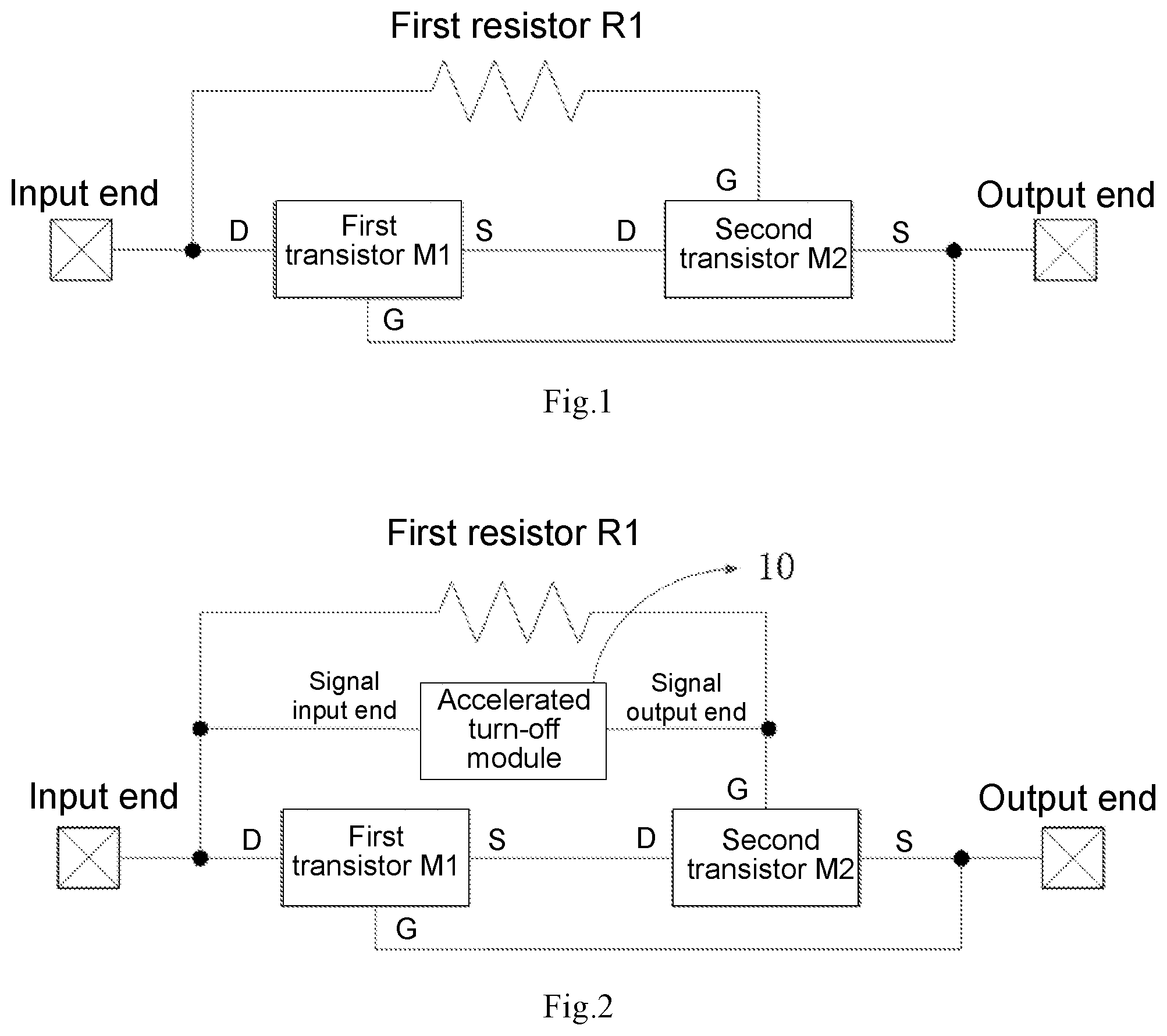
Provided is a blocking-type surge protector for accelerated turn-off, comprising: a first transistor (M 1 ), a drain electrode thereof connected to a first port; a second transistor (M 2 ), a drain electrode thereof connected to a source electrode of the first transistor (M 1 ), and a source electrode thereof connected to a gate electrode of the first transistor (M 1 ), the source electrode thereof being further connected to a second port; a first resistor (R 1 ), connected between the drain electrode of the first transistor (M 1 ) and the gate electrode of the second transistor (M 2 ); and an accelerated turn-off module ( 10 ), connected between the drain electrode of the first transistor (M 1 ) and the gate electrode of the second transistor (M 2 ).
Claims (9)
1 . A blocking-type surge protector having accelerated turn-off arranged between a first port and a second port, comprising: a first transistor, a drain electrode of the first transistor is connected to the first port; a second transistor, a drain electrode of the second transistor is connected to a source electrode of the first transistor, a source electrode of the second transistor is connected to a gate electrode of the first transistor, and the source electrode of the second transistor is connected to the second port; a first resistor, connected between the drain electrode of the first transistor and a gate electrode of the second transistor; an accelerated turn-off module, connected between the drain electrode of the first transistor and the gate electrode of the second transistor; wherein when a surge occurs, a current flowing through the accelerated turn-off module charges a parasitic capacitance of the gate electrode of the second transistor, such that a gate voltage of the second transistor quickly rises, so as to increase turn-off speed of blocking-type surge protector; a third transistor, wherein a source electrode of the third transistor is connected to the source electrode of the second transistor, a gate electrode of the third transistor is connected to the source electrode of the first transistor, and a drain electrode of the third transistor is connected to the second port; and a second resistor, connected between the gate electrode of the second transistor and the drain electrode of the third transistor; wherein the accelerated turn-off module comprises a first accelerated turn-off unit and a second accelerated turn-off unit; the first accelerated turn-off unit comprises: a first diode, wherein a negative terminal of the first diode is connected to the drain electrode of the first transistor; and a second diode, wherein a positive terminal of the second diode is connected to a positive terminal of the first diode, and a negative terminal of the second diode is connected to the gate electrode of the second transistor; the second accelerated turn-off unit comprises: a third diode, wherein a negative terminal of the third diode is connected to the gate electrode of the second transistor; and a fourth diode, wherein a positive terminal of the fourth diode is connected to a positive terminal of the third diode, and a negative terminal of the fourth diode is connected to the drain electrode of the third transistor; wherein the current of the blocking-type surge protector flows from the first port to the second port, or from the second port to the first port.
Show 8 dependent claims
2 . The blocking-type surge protector having accelerated turn-off of claim 1 , wherein the accelerated turn-off module comprises: a capacitor, connected between the drain electrode of the first transistor and the gate electrode of the second transistor; wherein the current of the blocking-type surge protector flows from the first port to the second port.
3 . The blocking-type surge protector having accelerated turn-off of claim 1 , wherein the accelerated turn-off module comprises: a first diode, wherein a positive terminal of the first diode is connected to the gate electrode of the second transistor, and a negative terminal of the first diode is connected to the drain electrode of the first transistor; wherein the current of the blocking-type surge protector flows from the first port to the second port.
4 . The blocking-type surge protector having accelerated turn-off of claim 1 or 3 , further comprising: a fourth transistor, wherein a source electrode of the fourth transistor is connected to the source electrode of the second transistor, a drain electrode of the fourth transistor is connected to the gate electrode of the first transistor, and a gate electrode of the fourth transistor is connected to the drain electrode of the second transistor; a third resistor, connected between the gate electrode of the fourth transistor and the drain electrode of the fourth transistor; the current of the blocking-type surge protector flows from the first port to the second port.
5 . The blocking-type surge protector having accelerated turn-off of claim 1 , further comprising: a fourth transistor, wherein a source electrode of the fourth transistor is connected to a source electrode of the second transistor, a drain electrode of the fourth transistor is connected to the gate electrode of the first transistor, and a gate electrode of the fourth transistor is connected to the drain electrode of the second transistor; a third resistor, connected between the gate electrode of the fourth transistor and the drain electrode of the fourth transistor; a fifth transistor, wherein a gate electrode of the fifth transistor is connected to the source electrode of the second transistor, a source electrode of the fifth transistor is connected to the drain electrode of the second transistor, and a drain electrode of the fifth transistor is connected to the gate electrode of the third transistor; a fourth resistor, connected between the drain electrode of the fifth transistor and the gate electrode of the fifth transistor.
6 . The blocking-type surge protector having accelerated turn-off of claim 1 , wherein the accelerated turn-off module comprises: a sixth transistor, wherein a gate electrode of the sixth transistor is connected to a source electrode of the sixth transistor, the source electrode of the sixth transistor is connected to the gate electrode of the second transistor, and a drain electrode of the sixth transistor is connected to the drain electrode of the first transistor; the current of the blocking-type surge protector flows from the first port to the second port.
7 . The blocking-type surge protector having accelerated turn-off of claim 1 , wherein the first transistor is a depletion-type NMOS transistor; the second transistor is a P-type junction field-effect transistor; the first resistor is a polysilicon resistor.
8 . The blocking-type surge protector having accelerated turn-off of claim 6 , wherein the sixth transistor is an enhancement-type NMOS transistor.
9 . The blocking-type surge protector having accelerated turn-off of claim 4 , wherein the fourth transistor is an enhancement-type NMOS transistor; the third resistor is a polysilicon resistor.
Full Description
Show full text →
BACKGROUND OF THE INVENTION
1. Field of the Invention The present invention relates to the field of surge protection technology, and more particularly, to a blocking-type surge protector having accelerated turn-off. 2. Description of the Related Art In electronic circuits, power surges or transient overvoltages can occur due to lightning strikes, power line coupling, power line induction, or ground bounce. When the surge is sufficiently high, it can cause serious damage to electronic devices such as computers and telephones. Similarly, it can also reduce the lifetime of the equipment. Currently, for computers and other high-speed data transmission lines, a blocking-type surge protector is chosen to protect the backend load. The blocking-type surge protector is connected in series with the load to provide targeted protection. When it reaches the triggering value, it changes its state, redirecting the surge through primary protection paths such as gas discharge tubes, effectively blocking transient surges from entering the protected equipment. The construction of the blocking-type surge protector in existing technology is shown in . It consists of the first transistor M 1 , the second transistor M 2 , and the first resistor R 1 . The first transistor M 1 is a depletion-type NMOS, and the second transistor M 2 is a P-type JFET. The first resistor R 1 is usually a polysilicon resistor. The drain electrode of the first transistor M 1 is connected to the gate electrode of the second transistor M 2 through the first resistor R 1 , which typically has a resistance value of several hundred kΩs and serves as a current-limiting element during the off state of the blocking-type surge protector. However, at the same time, the first resistor R 1 and the parasitic capacitance of the gate electrode of the second transistor M 2 connected therewith form a series RC circuit. Due to the relatively large resistance value, the time constant of the series RC circuit is large, resulting in slow charging of the parasitic capacitance of the gate electrode and slow rise of the gate voltage of the second transistor M 2 . This leads to a slow turn-off speed of the blocking-type surge protector, typically taking about 1 us to fully enter the off state. During this process, surge current can still flow through the blocking-type surge protector to the protected load, posing a safety risk to the load circuit.
SUMMARY OF THE INVENTION
This invention aims to provide a blocking-type surge protector having accelerated turn-off. By means of introducing the accelerated turn-off module into a circuit, the turn-off speed of the blocking-type surge protector is greatly increased and a current flowing to an output end during the turn-off process is reduced, thereby providing finer and excellent surge protection for the post-stage load. A blocking-type surge protector having accelerated turn-off arranged between a first port and a second port, comprising: a first transistor, a drain electrode of the first transistor is connected to the first port; a second transistor, a drain electrode of the second transistor is connected to a source electrode of the first transistor, a source electrode of the second transistor is connected to a gate electrode of the first transistor, and the source electrode of the second transistor is connected to the second port; a first resistor, connected between the drain electrode of the first transistor and a gate electrode of the second transistor; an accelerated turn-off module, connected between the drain electrode of the first transistor and the gate electrode of the second transistor; wherein when a surge occurs, a current flowing through the accelerated turn-off module charges a parasitic capacitance of the gate electrode of the second transistor, such that a gate voltage of the second transistor quickly rises, so as to increase turn-off speed of blocking-type surge protector. Further, the accelerated turn-off module comprises: a capacitor, connected between the drain electrode of the first transistor and the gate electrode of the second transistor; wherein the current of the blocking-type surge protector flows from the first port to the second port. Further, the accelerated turn-off module comprises: a first diode, wherein a positive terminal of the first diode is connected to the gate electrode of the second transistor, and a negative terminal of the first diode is connected to the drain electrode of the first transistor; wherein the current of the blocking-type surge protector flows from the first port to the second port. Further, the blocking-type surge protector having accelerated turn-off comprises: a third transistor, wherein a source electrode of the third transistor is connected to the source electrode of the second transistor, a gate electrode of the third transistor is connected to the source electrode of the first transistor, and a drain electrode of the third transistor is connected to the second port; a second resistor, connected between the gate electrode of the second transistor and the drain electrode of the third transistor; the accelerated turn-off module comprises a first accelerated turn-off unit and a second accelerated turn-off unit; the first accelerated turn-off unit comprises: a first diode, wherein a negative terminal of the first diode is connected to the drain electrode of the first transistor; a second diode, wherein a positive terminal of the second diode is connected to a positive terminal of the first diode, and a negative terminal of the second diode is connected to the gate electrode of the second transistor; the second accelerated turn-off unit comprises: a third diode, wherein a negative terminal of the third diode is connected to the gate electrode of the second transistor; a fourth diode, wherein a positive terminal of the fourth diode is connected to a positive terminal of the third diode, and a negative terminal of the fourth diode is connected to the drain electrode of the third transistor; the current of the blocking-type surge protector flows from the first port to the second port, or from the second port to the first port. Further, the blocking-type surge protector having accelerated turn-off comprises: a fourth transistor, wherein a source electrode of the fourth transistor is connected to the source electrode of the second transistor, a drain electrode of the fourth transistor is connected to the gate electrode of the first transistor, and a gate electrode of the fourth transistor is connected to the drain electrode of the second transistor; a third resistor, connected between the gate electrode of the fourth transistor and the drain electrode of the fourth transistor; the current of the blocking-type surge protector flows from the first port to the second port. Further, the blocking-type surge protector having accelerated turn-off comprises: a fourth transistor, wherein a source electrode of the fourth transistor is connected to a source electrode of the second transistor, a drain electrode of the fourth transistor is connected to the gate electrode of the first transistor, and a gate electrode of the fourth transistor is connected to the drain electrode of the second transistor; a third resistor, connected between the gate electrode of the fourth transistor and the drain electrode of the fourth transistor; a fifth transistor, wherein a gate electrode of the fifth transistor is connected to the source electrode of the second transistor, a source electrode of the fifth transistor is connected to the drain electrode of the second transistor, and a drain electrode of the fifth transistor is connected to the gate electrode of the third transistor; a fourth resistor, connected between the drain electrode of the fifth transistor and the gate electrode of the fifth transistor. Further, the accelerated turn-off module comprises: a sixth transistor, wherein a gate electrode of the sixth transistor is connected to a source electrode of the sixth transistor, the source electrode of the sixth transistor is connected to the gate electrode of the second transistor, and a drain electrode of the sixth transistor is connected to the drain electrode of the first transistor; the current of the blocking-type surge protector flows from the first port to the second port. Further, the first transistor is a depletion-type NMOS transistor; the second transistor is a P-type junction field-effect transistor; the first resistor is usually a polysilicon resistor. Further, the sixth transistor is an enhancement-type NMOS transistor. Further, the fourth transistor is an enhancement-type NMOS transistor; the third resistor is a polysilicon resistor. The benefit effect of the invention is as follows. A blocking-type surge protector for accelerated turn-off is provided. By means of introducing the accelerated turn-off module into a circuit, the turn-off speed of the blocking-type surge protector is greatly increased and a current flowing to an output end during the turn-off process is reduced, thereby providing finer and excellent surge protection for the post-stage load.
BRIEF DESCRIPTION OF THE DRAWINGS
shows the circuit structure of the blocking-type surge protector in the prior art; shows the circuit structure of the blocking-type surge protector having accelerated turn-off of the invention; shows the circuit diagram of an embodiment of the blocking-type surge protector having accelerated turn-off of the invention; shows the turn-off current waveform of the circuit design in the prior art and that of the circuit design of the invention; shows the turn-off voltage waveform of the circuit design in the prior art and that of the circuit design of the invention; shows the circuit diagram of another embodiment of the blocking-type surge protector having accelerated turn-off of the invention; shows the circuit diagram of another embodiment of the blocking-type surge protector having accelerated turn-off of the invention; shows the circuit diagram of another embodiment of the blocking-type surge protector having accelerated turn-off of the invention; shows the circuit diagram of another embodiment of the blocking-type surge protector having accelerated turn-off of the invention; shows the circuit diagram of another embodiment of the blocking-type surge protector having accelerated turn-off of the invention; shows the circuit diagram of another embodiment of the blocking-type surge protector having accelerated turn-off of the invention.
DETAILED DESCRIPTION
The following, in conjunction with the accompanying drawings of the embodiments of the invention, provides a clear and complete description of the technical solutions in the embodiments of the present invention. It is evident that the described embodiments are only a part of the embodiments of the invention, and not the entirety. Based on the embodiments of the present invention, all other embodiments that ordinary skilled persons in the art can obtain without exercising creative labor are within the scope of protection of the invention. It should be noted that, unless conflicting, the features in the embodiments of the invention can be combined with each other. The following, in conjunction with the accompanying drawings and specific embodiments, further illustrates the invention, but does not limit the scope of the invention. Example 1 Referring to , the invention provides a blocking-type surge protector having accelerated turn-off arranged between a first port and a second port, comprising: a first transistor M 1 , where a drain electrode of the first transistor is connected to the first port, a second transistor M 2 , where a drain electrode of the second transistor M 2 is connected to a source electrode of the first transistor M 1 , a source electrode of the second transistor M 2 is connected to a gate electrode of the first transistor M 1 , and the source electrode of the second transistor M 2 is connected to the second port; a first resistor R 1 , wherein a first end of the first resistor R 1 is connected to the drain electrode of the first transistor M 1 , and a second end of the first resistor R 1 is connected to the gate electrode of the second transistor M 2 , i.e., the first resistor R 1 is connected between the drain electrode of the first transistor M 1 and the gate electrode of the second transistor M 2 ; an accelerated turn-off module 10 , wherein a first end of the accelerated turn-off module 10 is connected to the drain electrode of the first transistor M 1 , and a second end of the accelerated turn-off module 10 is connected to the gate electrode of the second transistor M 2 , i.e., the accelerated turn-off module 10 is connected between the drain electrode of the first transistor M 1 and the gate electrode of the second transistor M 2 . The accelerated turn-off module 10 is used to increase the turn-off speed of the blocking surge protector. Preferably, the first transistor M 1 is a depletion-type NMOS transistor. Preferably, the second transistor M 2 is a P-type JFET, which is Junction Field-Effect Transistor (JFET). Preferably, the first resistor R 1 is usually a polysilicon resistor. Referring to , as a preferred embodiment of the example, the accelerated turn-off module 10 comprises: a capacitor C 1 , connected between the drain electrode of the first transistor M 1 and the gate electrode of the second transistor M 2 . The selection of the capacitance value of capacitor C 1 is related to a parasitic capacitance of the gate electrode of the second transistor M 2 and is generally in the range of tens of picofarads. Referring to , surge tests are conducted on the circuit design in the prior art in and that of the invention in . The current waveform is shown in , in which the circuit design in the prior art takes approximately 1.1 us to achieve complete turn-off, while the circuit design of the invention achieves complete turn-off in 0.3 us. Referring to , it shows the gate voltage waveform of the second transistor M 2 (P-type JFET) for both the circuit design in the prior art in and the circuit design of the invention in . The gate voltage rise rate of the circuit design of the invention is significantly faster than that of the traditional circuit. It can be seen that the accelerated turn-off module designed in the invention significantly increases the turn-off speed of the blocking-type surge protector. The current of the blocking-type surge protector flows from the first port to the second port, that is, the first port is the input end and the second port is the output end. Example 2 The main difference between the Example 2 and Example 1 is that the accelerated turn-off module 10 is a first diode D 1 . Referring to , the example provides a blocking-type surge protector having accelerated turn-off, comprising: a first transistor M 1 , a drain electrode of the first transistor M 1 is connected to a first port; a second transistor M 2 , a drain electrode of the second transistor M 2 is connected to a source electrode of the first transistor M 1 , a source electrode of the second transistor M 2 is connected to a gate electrode of the first transistor M 1 , and the source electrode of the second transistor M 2 is connected to a second port; a first resistor R 1 , a first end of the first resistor R 1 is connected to the drain electrode of the first transistor M 1 , and a second end of the first resistor R 1 is connected to the gate electrode of the second transistor M 2 ; that is, the first resistor R 1 is connected between the drain electrode of the first transistor M 1 and the gate electrode of the second transistor M 2 ; an accelerated turn-off module 10 , a first end of the accelerated turn-off module 10 is connected to the drain electrode of the first transistor M 1 , and a second end of the accelerated turn-off module 10 is connected to the gate electrode of the second transistor M 2 ; that is, the accelerated turn-off module 10 is connected between the drain electrode of the first transistor M 1 and the gate electrode of the second transistor M 2 ; wherein the accelerated turn-off module 10 comprises: a first diodes D 1 , a positive terminal of the first diodes D 1 is connected to the gate electrode of the second transistor M 2 , and a negative terminal of the first diode D 1 is connected to the drain electrode of the first transistor M 1 . Preferably, the first transistor M 1 is a depletion-type NMOS transistor. Preferably, the second transistor M 2 is a P-type JFET, which is Junction Field-Effect Transistor (JFET). Preferably, the first resistor R 1 is usually a polysilicon resistor. In applications such as RS232 interfaces, RS485 interfaces, CANBUS, etc., blocking-type surge protectors face the risk of external lightning surge voltages reaching several hundred volts. This requires the accelerated turn-off module in the circuit design to withstand these high voltages to avoid module breakdown and circuit short-circuiting. In Example 1, the capacitor C 1 , which serves as the accelerated turn-off module, faces challenges in achieving the required voltage withstand capability of several hundred volts in common semiconductor manufacturing processes. This poses challenges in the manufacturing and packaging of blocking-type surge protectors capable of withstanding high voltages. In this example, the accelerated turn-off module 10 is implemented by using diode D 1 . The positive terminal of diode D 1 is connected to the second port (i.e., the gate electrode of the second transistor M 2 ) of the signal, and the negative terminal of the diode D 1 is connected to the first port (i.e., the drain electrode of the first transistor M 1 ) of the signal. The voltage withstand capability and capacitance of the diode can be flexibly adjusted through semiconductor manufacturing processes, including but not limited to material resistivity, doping ion concentration, layout design, etc. This allows for a voltage withstand range from a few volts to several hundred volts and a capacitance range from a few picofarads to several hundred picofarads, greatly expanding the selection range for circuit design and enabling the circuit in Example 2 to withstand lightning surges of several hundred volts, thereby broadening the circuit's application range. The current of the blocking-type surge protector flows from the first port to the second port, that is, the first port is the input end and the second port is the output end. Example 3 This example is a development based on Example 2, in which the example is a bidirectional blocking-type surge protector having an accelerated turn-off module. The main difference is that between the second transistor M 2 and the second port, a third transistor M 3 is also connected, and a second resistor R 2 is added. Referring to , this example provides a bidirectional blocking-type surge protector having accelerated turn-off, comprising: a first transistor M 1 , a drain electrode of the first transistor M 1 is connected to the first port; a second transistor M 2 , a drain electrode of the second transistor M 2 is connected to a source electrode of the first transistor M 1 , and a source electrode of the second transistor M 2 is connected to a gate electrode of the first transistor M 1 ; the first resistor R 1 , a first end of the first resistor R 1 is connected to the drain electrode of the first transistor M 1 , and a second end of the first resistor R 1 is connected to a gate electrode of the second transistor M 2 , i.e., the first resistor R 1 is connected between the drain electrode of the first transistor M 1 and the gate electrode of the second transistor M 2 ; the accelerated turn-off module 10 includes a first accelerated turn-off unit 10 a and a second accelerated turn-off unit 10 b; the first accelerated turn-off unit 10 a , a first end of the first accelerated turn-off unit 10 a is connected to the drain electrode of the first transistor M 1 , and a second end of the first accelerated turn-off unit 10 a is connected to the gate electrode of the second transistor M 2 , i.e., the first accelerated turn-off unit 10 a is connected between the drain electrode of the first transistor M 1 and the gate electrode of the second transistor M 2 ; a third transistor M 3 , with a source electrode of the third transistor M 3 is connected to the source electrode of the second transistor M 2 , a gate electrode of the third transistor M 3 is connected to the source electrode of the first transistor M 1 , and a drain electrode of the third transistor M 3 is connected to the second port; a second resistor R 2 , a first end of the second resistor R 2 is connected to the gate electrode of the second transistor M 2 , and a second end of the second resistor R 2 is connected to the drain electrode of the third transistor M 3 , i.e., the second resistor R 2 is connected between the gate electrode of the second transistor M 2 and the drain electrode of the third transistor M 3 ; the second accelerated turn-off unit 10 b , a first end of the second accelerated turn-off unit 10 b is connected to the gate electrode of the second transistor M 2 , and a second end of the second accelerated turn-off unit 10 b is connected to the drain electrode of the third transistor M 3 , i.e., the second accelerated turn-off unit 10 b is connected between the gate electrode of the second transistor M 2 and the drain electrode of the third transistor M 3 ; the first accelerated turn-off unit 10 a includes: a first diode D 1 , a negative terminal of the first diode D 1 is connected to the drain electrode of the first transistor M 1 ; a second diode D 2 , a positive terminal of the second diode D 2 is connected to a positive terminal of the first diode D 1 , and a negative terminal of the second diode D 2 is connected to the gate electrode of the second transistor M 2 ; the second accelerated turn-off unit 10 b includes: a third diode D 3 , a negative terminal of the third diode D 3 is connected to the gate electrode of the second transistor M 2 ; a fourth diode D 4 , a positive terminal of the fourth diode D 4 is connected to a positive terminal of the third diode D 3 , and a negative terminal of the fourth diode D 4 is connected to the drain electrode of the third transistor M 3 . In this embodiment, the current of the surge protector flows from the first port to the second port, or from the second port to the first port. The two-directional accelerated turn-off units 10 a and 10 b are symmetrical and each consists of two diodes with opposite directions. The inclusion of diodes D 2 and D 3 is to prevent the short-circuiting of the second transistor M 2 by the forward diodes D 1 and D 4 when the gate voltage of the second transistor M 2 rises, ensuring that the circuit can be properly turned off. Preferably, the first transistor M 1 and the third transistor M 3 are depletion-type NMOS transistors. Preferably, the second transistor M 2 is a P-type JFET, which is Junction Field-Effect Transistor (JFET). Preferably, the first resistor R 1 and the second resistor R 2 are polysilicon resistors. Example 4 shows a circuit structure of a trigger current concentrator blocking-type surge protector having accelerated turn-off according to the invention. The circuit includes a fourth transistor M 4 and a third resistor R 3 , wherein the fourth transistor M 4 is an enhancement-type NMOS transistor, and the third resistor R 3 is usually a polysilicon resistor. The fourth transistor M 4 is connected between the gate electrode of the first transistor M 1 and the source electrode of the second transistor M 2 . Referring to , this example provides a trigger current concentrator blocking-type surge protector having accelerated turn-off, comprising: a first transistor M 1 , a drain electrode of the first transistor M 1 is connected to a first port; a second transistor M 2 , a drain electrode of the second transistor M 2 is connected to the source electrode of the first transistor M 1 , and a source electrode of the second transistor M 2 is connected to a second port; a first resistor R 1 , a first end of the first resistor R 1 is connected to the drain electrode of the first transistor M 1 , and a second end of the first resistor R 1 is connected to the gate electrode of the second transistor M 2 ; that is, the first resistor R 1 is connected between the drain electrode of the first transistor M 1 and the gate electrode of the second transistor M 2 ; an accelerated turn-off module 10 , a first end of the accelerated turn-off module 10 is connected to the drain electrode of the first transistor M 1 , and the second end of the accelerated turn-off module 10 is connected to the gate electrode of the second transistor M 2 , i.e., the accelerated turn-off module 10 is connected between the drain electrode of the first transistor M 1 and the gate electrode of the second transistor M 2 ; a fourth transistor M 4 , a source electrode of the fourth transistor M 4 is connected to a source electrode of the second transistor M 2 , a drain electrode of the fourth transistor M 4 is connected to the gate electrode of the first transistor M 1 , and the gate electrode of the fourth transistor M 4 is connected to the drain electrode of the second transistor M 2 ; a third resistor R 3 , a first end of the third resistor R 3 is connected to the gate electrode of the fourth transistor M 4 , and a second end of the third resistor R 3 is connected to the drain electrode of the fourth transistor M 4 , i.e., the third resistor R 3 is connected between the gate electrode of the second transistor M 2 and the drain electrode of the three transistor M 3 . Preferably, the first transistor M 1 is a depletion-type NMOS transistor. Preferably, the second transistor M 2 is a P-type JFET, which is Junction Field-Effect Transistor (JFET). Preferably, the first resistor R 1 is usually a polysilicon resistor. Preferably, the fourth transistor M 4 is an enhancement-type NMOS transistor. Preferably, the third resistor R 3 is usually a polysilicon resistor. Referring to , as a preferred embodiment of this example, the accelerated turn-off module 10 includes a first diode D 1 , a positive terminal is of the first transistor M 1 is connected to the gate electrode of the second transistor M 2 , and a negative terminal first diode D 1 is connected to the drain electrode of the first transistor M 1 . In the circuit, the fourth transistor M 4 and the third resistor R 3 are present in the circuit of the gate electrode of the first transistor M 1 . During the semiconductor manufacturing process, normal process variations can cause the threshold voltage of the first transistor M 1 to vary within a certain range. This leads to significant fluctuations in the triggering turn-off current of the whole circuit of the blocking-type surge protector, which is not conducive to stable and consistent product performance. However, the fourth transistor M 4 in the circuit effectively solves the aforementioned problem. This is because the threshold voltage fluctuations of the enhancement-type NMOS transistor can be precisely controlled during the manufacturing process, thereby keeping the variation of the threshold voltage within a small range. When there is a lightning surge at the first port, the voltage generated across the two ends of the current flowing through the second transistor M 2 reaches the threshold voltage of the fourth transistor M 4 . Only when M 4 is turned on, the whole circuit starts to turn off, thus avoiding the problem of inconsistent triggering turn-off current caused by fluctuations in the threshold voltage of the first transistor M 1 . The added accelerated turn-off module in this invention allows for a rapid increase in the voltage at the gate electrode of the second transistor M 2 , thereby causing the voltage across the two ends of the second transistor M 2 to rise quickly to reach the threshold voltage of the fourth transistor M 4 as soon as possible. This leads to the rapid activation of the fourth transistor M 4 , effectively accelerating the whole circuit turn-off process. The threshold voltage of the fourth transistor M 4 varies depending on the conduction resistance of the second transistor M 2 and the trigger turn-off current, typically around 1V. The third resistor R 3 is included to prevent a short circuit of the second transistor M 2 when the fourth transistor M 4 is activated, with a resistance value typically several hundred kΩs. The current of the blocking-type surge protector flows from the first port to the second port. The first port serves as the current input end, while the second port serves as the current output end. Example 5 This example is developed based on Example 4 and features a bidirectional blocking-type surge protection circuit having an accelerated turn-off. The main difference lies in a fourth transistor M 4 is further connected between the gate electrode of the first transistor M 1 and the source electrode of the second transistor M 2 . A third resistor R 3 is connected between the gate electrode and drain electrode of the fourth transistor M 4 . Additionally, a fifth transistor M 5 is connected between the gate electrode of the third transistor M 3 and the drain electrode of the second transistor M 2 , a fourth resistor R 4 is connected between the gate electrode and drain electrode of the fifth transistor M 5 . Referring to , this example provides a bidirectional blocking-type surge protector having accelerated turn-off, comprising: a first transistor M 1 , a drain electrode of the first transistor M 1 is connected to the first port; a second transistor M 2 , a drain electrode of the second transistor M 2 is connected to the source electrode of the first transistor M 1 , a source electrode of the second transistor M 2 is connected to the gate electrode of the first transistor M 1 , and the source electrode of the second transistor M 2 is connected to the second port; a first resistor R 1 , a first end of the first resistor R 1 is connected to the drain electrode of the first transistor M 1 , and a second end of the first transistor M 1 is connected to the gate electrode of the second transistor M 2 ; that is, the first resistor R 1 is connected between the drain electrode of the first transistor M 1 and the gate electrode of the second transistor M 2 ; a third transistor M 3 , a source electrode of the third transistor M 3 is connected to the source electrode of the second transistor M 2 , the gate electrode of the third transistor M 3 is connected to the source electrode of the first transistor M 1 , and the drain electrode of the third transistor M 3 is connected to the second port; a second resistor R 2 , a first end of the second resistor R 2 is connected to the gate electrode of the second transistor M 2 , and a second end of the second resistor R 2 is connected to the drain electrode of the third transistor M 3 ; that is, the second resistor R 2 is connected between the gate electrode of the second transistor M 2 and the drain electrode of the third transistor M 3 ; the accelerated turn-off module 10 includes a first accelerated turn-off unit 10 a and a second accelerated turn-off unit 10 b; wherein the first accelerated turn-off unit 10 a includes: a first diode D 1 , a negative terminal of the first diode D 1 is connected to the drain electrode of the first transistor M 1 ; a second diode D 2 , a positive terminal of the second diode D 2 is connected to a positive terminal of the first diode D 1 , and a negative terminal of the second diode D 2 is connected to the gate electrode of the second transistor M 2 ; wherein the second accelerated turn-off unit 10 b includes: a third diode D 3 , a negative terminal of the third diode D 3 is connected to the gate electrode of the second transistor M 2 ; a fourth diode D 4 , a positive terminal of the fourth diode D 4 is connected to a positive terminal of the third diode D 3 , and a negative terminal of the fourth diode D 4 connected to the drain electrode of the third transistor M 3 ; a fourth transistor M 4 , a source electrode of the fourth transistor M 4 is connected to the source electrode of the second transistor M 2 , the drain electrode of the fourth transistor M 4 is connected to the gate electrode of the first transistor M 1 , and the gate electrode of the fourth transistor M 4 is connected to the drain electrode of the second transistor M 2 ; a fifth transistor M 5 , a gate electrode of the fifth transistor M 5 is connected to the source electrode of the second transistor M 2 , a source electrode of the fifth transistor M 5 is connected to the drain electrode of the second transistor M 2 , and a drain electrode of the fifth transistor M 5 is connected to the gate electrode of the third transistor M 3 ; a third resistor R 3 , a first end of the third resistor R 3 is connected to the gate electrode of the fourth transistor M 4 , and a second end of the third resistor R 3 is connected to the drain electrode of the fourth transistor M 4 ; a fourth resistor R 4 , a first end of the fourth resistor R 4 is connected to the drain electrode of the fifth transistor M 5 , and the second end of the fourth resistor R 4 is connected to the gate electrode of the fifth transistor M 5 ; that is, the fourth resistor R 4 is connected between the drain electrode of the fifth transistor M 5 and the gate electrode of the fifth transistor M 5 . In this example, the enhancement-type NMOS transistor M 4 and resistor R 3 connected to the gate circuit of the first transistor M 1 are used to solve the problem of inconsistent trigger turn-off current values from the first port to the second port caused by fluctuations in the M 1 threshold voltage. The first accelerated turn-off unit 10 a is used to accelerate the turn-off speed when lightning surges occur in the direction from the first port to the second port. The enhancement-type NMOS transistor M 5 and resistor R 4 connected to the gate circuit of the third transistor M 3 are used to solve the problem of inconsistent trigger turn-off current values from the second port to the first port caused by fluctuations in the M 3 threshold voltage. The second accelerated turn-off unit 10 b is used to accelerate the turn-off speed when lightning surges occur in the direction from the second port to the first port. Preferably, the first transistor M 1 and the third transistor M 3 are depletion-type NMOS transistors. Preferably, the second transistor M 2 is a P-type JFET, which is Junction Field-Effect Transistor (JFET). Preferably, the first resistor R 1 and the second resistor R 2 is polysilicon resistors. Preferably, the fourth transistor M 4 and the fifth transistor M 5 are enhancement-type NMOS transistors. Example 6 The main difference between this example and Example 1 is that the accelerated turn-off module 10 is a sixth transistor M 6 . Referring to , this example provides a blocking-type surge protector having accelerated turn-off, comprising: a first transistor M 1 , a drain electrode of the first transistor is connected to the first port; a second transistor M 2 , a drain electrode of the second transistor M 2 is connected to a source electrode of the first transistor M 1 , a source electrode of the second transistor M 2 is connected to a gate electrode of the first transistor M 1 , and the source electrode of the second transistor M 2 is connected to the second port; a first resistor R 1 , a first end of the first resistor R 1 is connected to the drain electrode of the first transistor M 1 , and a second end of the first resistor R 1 is connected to the gate electrode of the second transistor M 2 ; that is, the first resistor R 1 is connected between the drain electrode of the first transistor M 1 and the gate electrode of the second transistor M 2 ; an accelerated turn-off module 10 , a first port of the accelerated turn-off module 10 connected to the drain electrode of the first transistor M 1 , and the second port of the accelerated turn-off module 10 is connected to the gate electrode of the second transistor M 2 ; the accelerated turn-off module 10 is connected between the drain electrode of the first transistor M 1 and the gate electrode of the second transistor M 2 ; wherein, the accelerated turn-off module 10 includes: a sixth transistor M 6 , a gate electrode of the sixth transistor M 6 is connected to the source electrode of the sixth transistor M 6 , a source electrode of the sixth transistor M 6 is connected to the gate electrode of the second transistor M 2 , and the drain electrode of the sixth transistor M 6 is connected to the drain electrode of the first transistor M 1 . The current of the blocking-type surge protector flows from the first port to the second port. The first port serves as the current input end, while the second port serves as the current output end. Preferably, the first transistor M 1 is a depletion-type NMOS transistor. Preferably, the second transistor M 2 is a P-type JFET, which is Junction Field-Effect Transistor (JFET). Preferably, the first resistor R 1 is usually a polysilicon resistor. Preferably, the sixth transistor M 6 is an enhancement-type NMOS transistor. The above is merely a preferred embodiment of the invention, and should not be construed as limiting the implementation and scope of the invention. Those skilled in the art should be aware that any equivalent substitutions and obvious modifications made based on the disclosure and illustrations in this specification are included within the scope of the invention.
Figures (6)
Citations
This patent cites (7)
- US6970337
- US8254073
- US8487667
- US2009/0027822
- US2009/0122456
- US2009/0231773
- US2012/0280271