Smart Verify Algorithm for Improving Reliability for Ultra High-performance 3D NAND
Abstract
A memory device has control circuitry that is configured to perform a smart verify operation on the memory cells of a selected word line to acquire an initial programming voltage for programming subsequent word lines. Following completion of the smart verify operation, the control circuitry is configured to adjust a programming voltage by both a step size or one half of a step size and also an offset and then continue programming the memory cells of the selected word line.
Claims (14)
1 . A method of programming a memory device, comprising steps of: performing a smart verify operation on a selected wordline to acquire an initial programming voltage for programming subsequent wordlines, the smart verify operation including a plurality of program loops with programming pulses at programming voltages that increase by a step size between program loops, the program loops including verify operations at a smart verify low voltage and at a smart verify high voltage; and following completion of the smart verify operation, adjusting the programming voltage by both the step size or one half of the step size and an offset and then continuing programming of the selected wordline.
7 . A memory device, comprising: at least one memory block that includes a plurality of memory cells arranged in a plurality of wordlines; and control circuitry configured to program the memory cells of a selected wordline of the plurality of wordlines, the control circuitry being further configured to: perform a smart verify operation on the selected wordline, the smart verify operation including a plurality of program loops with programming pulses at programming voltages that increase by a step size between program loops, the program loops including verify operations at a smart verify low voltage and a smart verify high voltage to acquire an initial programming voltage for programming subsequent wordlines; and following completion of the smart verify operation, adjust the programming voltage by both the step size or one half of the step size and an offset and then continue programming of the selected wordline.
13 . An apparatus, comprising: at least one memory block that includes a plurality of memory cells arranged in a plurality of wordlines; and a means for programming user data into the memory cells of a selected word line of the plurality of wordlines, the programming means being configured to: perform a smart verify operation on the selected wordline, the smart verify operation including a plurality of program loops with programming pulses at programming voltages that increase by a step size between program loops, the program loops including verify operations at a smart verify low voltage and a smart verify high voltage to acquire an initial programming voltage for programming subsequent wordlines; and following completion of the smart verify operation, adjust the programming voltage by both the step size or one half of the step size and an offset and then perform a program on the selected wordline.
Show 11 dependent claims
2 . The method as set forth in claim 1 , further including the step of: performing a program operation that has no smart verify operation and begins with the programming voltage being set at the initial programming voltage on another wordline.
3 . The method as set forth in claim 1 , wherein the smart verify operation on the selected wordline ends when the verify operation at the smart verify low voltage fails.
4 . The method as set forth in claim 3 , wherein: in response to the verify operation at the smart verify low voltage failing, the method further including the step of determining if the verify operation at the smart verify high voltage fails.
5 . The method as set forth in claim 4 , wherein in response to the verify operation at the smart verify high voltage fails, the step of adjusting the programming voltage by both the step size or one half of the step size and the offset and then continuing programming includes adjusting the programming voltage by both one half of the step size and the offset.
6 . The method as set forth in claim 5 , wherein: in response to the verify operation at the verify high voltage passing, the step of adjusting the programming voltage by both the step size or one half of the step size and the offset and then continuing programming includes adjusting the programming voltage by both the step size and the offset.
8 . The memory device as set forth in claim 7 , wherein the control circuitry is further configured to: perform a program operation that has no smart verify operation and begins with the programming voltage being set at the initial programming voltage on another wordline.
9 . The memory device as set forth in claim 7 , wherein the control circuitry is further configured to end the smart verify operation when the verify operation fails at the smart verify low voltage.
10 . The memory device as set forth in claim 9 , wherein the control circuitry is further configured to: in response to the verify operation failing at the smart verify low voltage, determine if the verify operation fails at the smart verify high voltage.
11 . The memory device as set forth in claim 9 , wherein in response to the verify operation failing at the smart verify high voltage, the control circuitry is further configured to adjust the programming voltage by both one half of the step size and the offset.
12 . The memory device as set forth in claim 11 , wherein in response to the verify operation passing at the smart verify high voltage, the control circuitry is further configured to adjust the programming voltage by both the step size and the offset.
14 . The apparatus as set forth in claim 13 , wherein the programming means is further configured to perform a program operation that has no smart verify operation and begins with the programming voltage being set at the initial programming voltage on another wordline.
Full Description
Show full text →
BACKGROUND
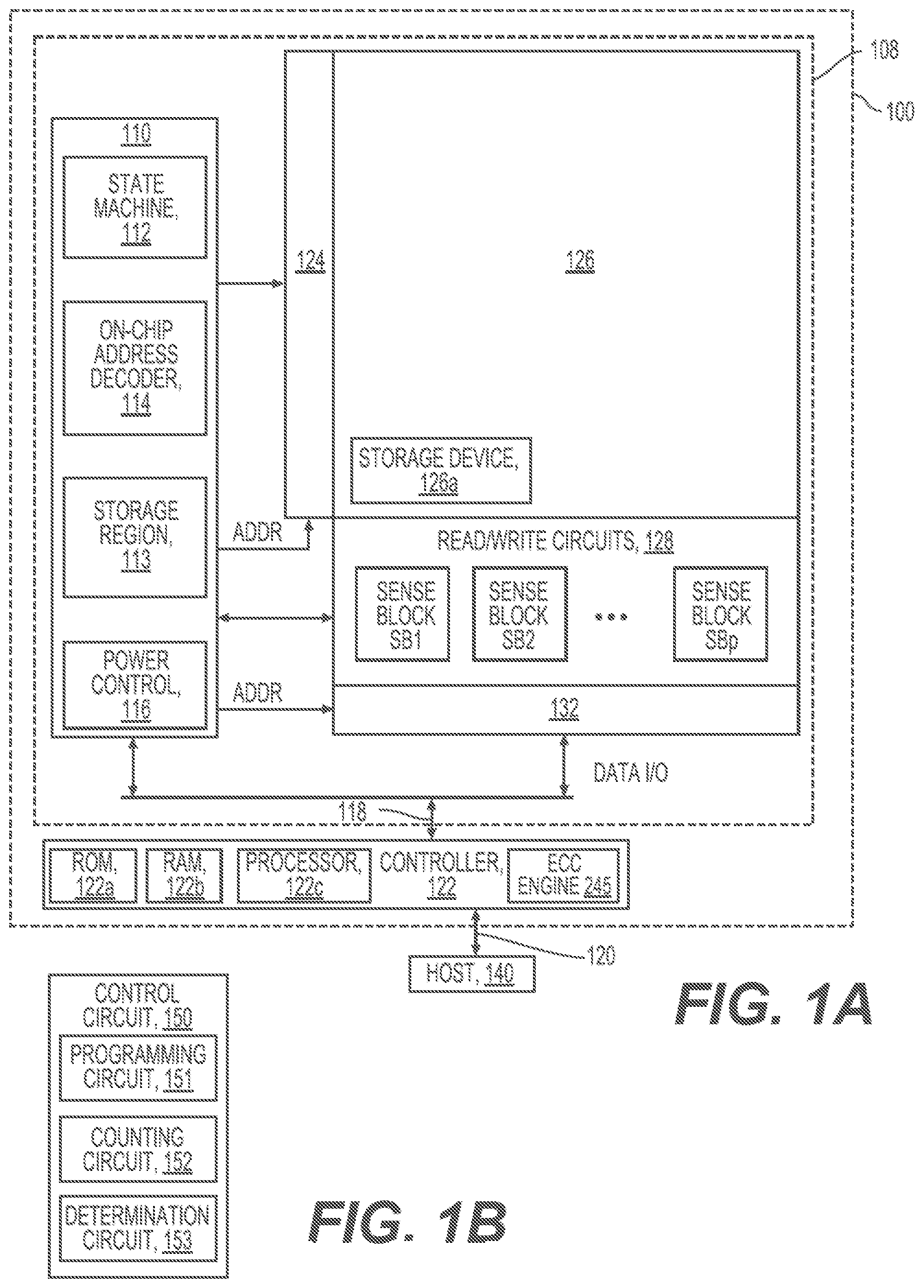
1. Field The present disclosure is related generally to memory devices and more particularly to techniques for programming of memory cells of a memory device. 2. Related Art Semiconductor memory is widely used in various electronic devices, such as cellular telephones, digital cameras, personal digital assistants, medical electronics, mobile computing devices, servers, solid state drives, non-mobile computing devices and other devices. Semiconductor memory may comprise non-volatile memory or volatile memory. A non-volatile memory allows information to be stored and retained even when the non-volatile memory is not connected to a source of power, e.g., a battery. NAND memory devices include a chip with a plurality of memory blocks, each of which includes an array of memory cells arranged in a plurality of word lines. Programming the memory cells of a word line to retain data typically occurs in a plurality of program loops, each of which includes the application of a programming pulse to a control gate of the word line and, optionally, a verify operation to sense the threshold voltages of the memory cells being programmed. In many programming techniques, the programming pulse has an initial programming voltage in a first program loop, and then the voltage of the programming pulse increases incrementally between program loops until programming is completed. An optimal value for the initial programming voltage varies across the plurality of memory blocks in the chip and may also vary among the word lines of a single memory block. If the initial programming voltage is set too high, overprogramming of some memory cells can occur, but if it is set too low, programming performance may suffer.
SUMMARY
This section provides a general summary of the present disclosure and is not a comprehensive disclosure of its full scope or all of its features and advantages. An object of the present disclosure is to provide a memory apparatus and a method of operation of the memory apparatus that address and overcome shortcomings described herein. Accordingly, it is an aspect of the present disclosure to provide a method of programming a memory device. The method comprises the steps of: performing a smart verify operation on a wordline to acquire programming voltage information; and continuing programming of the wordline based on the programming voltage information acquired during the smart verify operation. Accordingly, it is an aspect of the present disclosure to provide a memory device. The memory device comprises: at least one memory block that includes a plurality of memory cells arranged in a plurality of word lines; and control circuitry configured to program the memory cells of the at least one memory block in a plurality of program loops. The control circuitry is further configured to: perform a smart verify operation on a wordline to acquire programming voltage information; and continue programming of the wordline based on the programming voltage information acquired during the smart verify operation. Accordingly, it is an aspect of the present disclosure to provide an apparatus. The apparatus comprises: at least one memory block that includes a plurality of memory cells arranged in a plurality of word lines; and a means for programming user data into the plurality of memory cells and configured to program the memory cells of the at least one memory block. The programming means is configured to: perform a smart verify operation on a portion of a wordline to acquire an initial programming voltage; and perform a program operation starting with the initial programming voltage on a remaining portion of the wordline.
BRIEF DESCRIPTION OF THE DRAWINGS
A more detailed description is set forth below with reference to example embodiments depicted in the appended figures. Understanding that these figures depict only example embodiments of the disclosure and are, therefore, not to be considered limiting of its scope. The disclosure is described and explained with added specificity and detail through the use of the accompanying drawings in which: A is a block diagram of an example memory device; B is a block diagram of an example control circuit; depicts blocks of memory cells in an example two-dimensional configuration of the memory array of A ; A and B depict cross-sectional views of example floating gate memory cells in NAND strings; A and B depict cross-sectional views of example charge-trapping memory cells in NAND strings; depicts an example block diagram of the sense block SB 1 of ; A is a perspective view of a set of blocks in an example three-dimensional configuration of the memory array of ; B depicts an example cross-sectional view of a portion of one of the blocks of A ; C depicts a plot of memory hole diameter in the stack of B ; D depicts a close-up view of region 622 of the stack of B ; A depicts a top view of an example word line layer WLL 0 of the stack of B ; B depicts atop view of an example top dielectric layer DL 116 of the stack of B ; depicts a threshold voltage distribution of a page of memory cells programmed to one bit per memory cell (SLC); depicts a threshold voltage distribution of a page of memory cells programmed to three bits per memory cell (TLC); depicts a threshold voltage distribution of a page of memory cells programmed to four bits per memory cell (QLC); depicts a voltage waveform of the voltage applied to a control gate of a selected word line during a programming operation; depicts a voltage waveform of the voltages applied to a control gate of a selected word line during and immediately after a smart verify operation; depicts a threshold voltage distribution of a plurality of memory cells before and following a plurality of program loops of a smart verify operation; illustrates an exemplary waveform of states S 1 to S 7 threshold voltage width versus starting programming pulse; generally illustrates how periodic over programming may occur for large program loop step size with the implementation of smart program count verify; and depicts the steps of the steps of a smart-verify periodic over program protection flow according to another example embodiment of the present disclosure. DESCRIPTION OF THE ENABLING EMBODIMENTS Using large program voltage step sizes is one way to improve performance of a memory device. However, there is a tradeoff between performance and reliability when using larger program voltage step sizes (ΔVpgm). For example, Vt distributions become wider and the bit error rate (BER) increases. In addition, when the ΔVpgm becomes comparable to or greater than the state-to-state verify level spacing, another issue arises called periodic overprogramming (OP). Periodic OP occurs when the Vt-widths become periodically wider across different starting program voltages (VPGMU). Periodic OP can also be exacerbated by wordline/block/die variations. Smart verify (SV) is a mode that involves finding the most suitable VPGM for wordlines. When SV mode is enabled, periodic OP may be reduced on SV application wordlines and strings, but the SV acquisition wordline and string may still suffer from periodic OP. In general, periodic OP is worse for the SV acquisition wordlines and string than for the other wordlines and strings where SV is applied. This is due to the SV information being applied only to the SV application wordlines and strings, and there being no adjustment on the SV acquisition wordlines and string. To address this, embodiments disclosed herein are directed to an improved SV operation. To explore the foregoing in further detail, A will now be described. A is a block diagram of an example memory device 100 is configured to operate according to the programming techniques of the present disclosure. The memory die 108 includes a memory structure 126 of memory cells, such as an array of memory cells, control circuitry 110 , and read/write circuits 128 . The memory structure 126 is addressable by word lines via a row decoder 124 and by bit lines via a column decoder 132 . The read/write circuits 128 include multiple sense blocks SB 1 , SB 2 , . . . SBp (sensing circuitry) and allow a page of memory cells to be read or programmed in parallel. Typically, a controller 122 is included in the same memory device 100 (e.g., a removable storage card) as the one or more memory die 108 . Commands and data are transferred between the host 140 and controller 122 via a data bus 120 , and between the controller and the one or more memory die 108 via lines 118 . The memory structure 126 can be two-dimensional or three-dimensional. The memory structure 126 may comprise one or more array of memory cells including a three-dimensional array. The memory structure 126 may comprise a monolithic three-dimensional memory structure in which multiple memory levels are formed above (and not in) a single substrate, such as a wafer, with no intervening substrates. The memory structure 126 may comprise any type of non-volatile memory that is monolithically formed in one or more physical levels of arrays of memory cells having an active area disposed above a silicon substrate. The memory structure 126 may be in a non-volatile memory device having circuitry associated with the operation of the memory cells, whether the associated circuitry is above or within the substrate. The control circuitry 110 cooperates with the read/write circuits 128 to perform memory operations on the memory structure 126 , and includes a state machine 112 , an on-chip address decoder 114 , and a power control module 116 . The state machine 112 provides chip-level control of memory operations. A storage region 113 may, for example, be provided for programming parameters. The programming parameters may include a program voltage, a program voltage bias, position parameters indicating positions of memory cells, contact line connector thickness parameters, a verify voltage, and/or the like. The position parameters may indicate a position of a memory cell within the entire array of NAND strings, a position of a memory cell as being within a particular NAND string group, a position of a memory cell on a particular plane, and/or the like. The contact line connector thickness parameters may indicate a thickness of a contact line connector, a substrate or material that the contact line connector is comprised of, and/or the like. The on-chip address decoder 114 provides an address interface between that used by the host or a memory controller to the hardware address used by the decoders 124 and 132 . The power control module 116 controls the power and voltages supplied to the word lines and bit lines during memory operations. It can include drivers for word lines, SGS and SGD transistors, and source lines. The sense blocks can include bit line drivers, in one approach. An SGS transistor is a select gate transistor at a source end of a NAND string, and an SGD transistor is a select gate transistor at a drain end of a NAND string. In some embodiments, some of the components can be combined. In various designs, one or more of the components (alone or in combination), other than memory structure 126 , can be thought of as at least one control circuit which is configured to perform the actions described herein. For example, a control circuit may include any one of, or a combination of, control circuitry 110 , state machine 112 , decoders 114 / 132 , power control module 116 , sense blocks SBb, SB 2 , . . . , SBp, read/write circuits 128 , controller 122 , and so forth. The control circuits can include a programming circuit configured to perform a program and verify operation for one set of memory cells, wherein the one set of memory cells comprises memory cells assigned to represent one data state among a plurality of data states and memory cells assigned to represent another data state among the plurality of data states; the program and verify operation comprising a plurality of program and verify iterations; and in each program and verify iteration, the programming circuit performs programming for the one selected word line after which the programming circuit applies a verification signal to the selected word line. The control circuits can also include a counting circuit configured to obtain a count of memory cells which pass a verify test for the one data state. The control circuits can also include a determination circuit configured to determine, based on an amount by which the count exceeds a threshold, if a programming operation is completed. For example, B is a block diagram of an example control circuit 150 which comprises a programming circuit 151 , a counting circuit 152 , and a determination circuit 153 . The off-chip controller 122 may comprise a processor 122 c , storage devices (memory) such as ROM 122 a and RAM 122 b and an error-correction code (ECC) engine 245 . The ECC engine can correct a number of read errors which are caused when the upper tail of a Vth distribution becomes too high. However, uncorrectable errors may exist in some cases. The techniques provided herein reduce the likelihood of uncorrectable errors. The storage device(s) 122 a , 122 b comprise, code such as a set of instructions, and the processor 122 c is operable to execute the set of instructions to provide the functionality described herein. Alternately or additionally, the processor 122 c can access code from a storage device 126 a of the memory structure 126 , such as a reserved area of memory cells in one or more word lines. For example, code can be used by the controller 122 to access the memory structure 126 such as for programming, read and erase operations. The code can include boot code and control code (e.g., set of instructions). The boot code is software that initializes the controller 122 during a booting or startup process and enables the controller 122 to access the memory structure 126 . The code can be used by the controller 122 to control one or more memory structures 126 . Upon being powered up, the processor 122 c fetches the boot code from the ROM 122 a or storage device 126 a for execution, and the boot code initializes the system components and loads the control code into the RAM 122 b . Once the control code is loaded into the RAM 122 b , it is executed by the processor 122 c . The control code includes drivers to perform basic tasks such as controlling and allocating memory, prioritizing the processing of instructions, and controlling input and output ports. Generally, the control code can include instructions to perform the functions described herein including the steps of the flowcharts discussed further below and provide the voltage waveforms including those discussed further below. In one embodiment, the host is a computing device (e.g., laptop, desktop, smartphone, tablet, digital camera) that includes one or more processors, one or more processor readable storage devices (RAM, ROM, flash memory, hard disk drive, solid state memory) that store processor readable code (e.g., software) for programming the one or more processors to perform the methods described herein. The host may also include additional system memory, one or more input/output interfaces and/or one or more input/output devices in communication with the one or more processors. Other types of non-volatile memory in addition to NAND flash memory can also be used. Semiconductor memory devices include volatile memory devices, such as dynamic random access memory (“DRAM”) or static random access memory (“SRAM”) devices, non-volatile memory devices, such as resistive random access memory (“ReRAM”), electrically erasable programmable read only memory (“EEPROM”), flash memory (which can also be considered a subset of EEPROM), ferroelectric random access memory (“FRAM”), and magnetoresistive random access memory (“MRAM”), and other semiconductor elements capable of storing information. Each type of memory device may have different configurations. For example, flash memory devices may be configured in a NAND or a NOR configuration. The memory devices can be formed from passive and/or active elements, in any combinations. By way of non-limiting example, passive semiconductor memory elements include ReRAM device elements, which in some embodiments include a resistivity switching storage element, such as an anti-fuse or phase change material, and optionally a steering element, such as a diode or transistor. Further by way of non-limiting example, active semiconductor memory elements include EEPROM and flash memory device elements, which in some embodiments include elements containing a charge storage region, such as a floating gate, conductive nanoparticles, or a charge storage dielectric material. Multiple memory elements may be configured so that they are connected in series or so that each element is individually accessible. By way of non-limiting example, flash memory devices in a NAND configuration (NAND memory) typically contain memory elements connected in series. A NAND string is an example of a set of series-connected transistors comprising memory cells and SG transistors. A NAND memory array may be configured so that the array is composed of multiple memory strings in which a string is composed of multiple memory elements sharing a single bit line and accessed as a group. Alternatively, memory elements may be configured so that each element is individually accessible, e.g., a NOR memory array. NAND and NOR memory configurations are examples, and memory elements may be otherwise configured. The semiconductor memory elements located within and/or over a substrate may be arranged in two or three dimensions, such as a two-dimensional memory structure or a three-dimensional memory structure. In a two-dimensional memory structure, the semiconductor memory elements are arranged in a single plane or a single memory device level. Typically, in a two-dimensional memory structure, memory elements are arranged in a plane (e.g., in an x-y direction plane) which extends substantially parallel to a major surface of a substrate that supports the memory elements. The substrate may be a wafer over or in which the layer of the memory elements is formed or it may be a carrier substrate which is attached to the memory elements after they are formed. As a non-limiting example, the substrate may include a semiconductor such as silicon. The memory elements may be arranged in the single memory device level in an ordered array, such as in a plurality of rows and/or columns. However, the memory elements may be arrayed in non-regular or non-orthogonal configurations. The memory elements may each have two or more electrodes or contact lines, such as bit lines and word lines. A three-dimensional memory array is arranged so that memory elements occupy multiple planes or multiple memory device levels, thereby forming a structure in three dimensions (i.e., in the x, y and z directions, where the z-direction is substantially perpendicular and the x- and y-directions are substantially parallel to the major surface of the substrate). As a non-limiting example, a three-dimensional memory structure may be vertically arranged as a stack of multiple two-dimensional memory device levels. As another non-limiting example, a three-dimensional memory array may be arranged as multiple vertical columns (e.g., columns extending substantially perpendicular to the major surface of the substrate, i.e., in the y direction) with each column having multiple memory elements. The columns may be arranged in a two-dimensional configuration, e.g., in an x-y plane, resulting in a three-dimensional arrangement of memory elements with elements on multiple vertically stacked memory planes. Other configurations of memory elements in three dimensions can also constitute a three-dimensional memory array. By way of non-limiting example, in a three-dimensional array of NAND strings, the memory elements may be coupled together to form a NAND string within a single horizontal (e.g., x-y) memory device level. Alternatively, the memory elements may be coupled together to form a vertical NAND string that traverses across multiple horizontal memory device levels. Other three-dimensional configurations can be envisioned wherein some NAND strings contain memory elements in a single memory level while other strings contain memory elements which span through multiple memory levels. Three-dimensional memory arrays may also be designed in a NOR configuration and in a ReRAM configuration. Typically, in a monolithic three-dimensional memory array, one or more memory device levels are formed above a single substrate. Optionally, the monolithic three-dimensional memory array may also have one or more memory layers at least partially within the single substrate. As a non-limiting example, the substrate may include a semiconductor such as silicon. In a monolithic three-dimensional array, the layers constituting each memory device level of the array are typically formed on the layers of the underlying memory device levels of the array. However, layers of adjacent memory device levels of a monolithic three-dimensional memory array may be shared or have intervening layers between memory device levels. Then again, two-dimensional arrays may be formed separately and then packaged together to form a non-monolithic memory device having multiple layers of memory. For example, non-monolithic stacked memories can be constructed by forming memory levels on separate substrates and then stacking the memory levels atop each other. The substrates may be thinned or removed from the memory device levels before stacking, but as the memory device levels are initially formed over separate substrates, the resulting memory arrays are not monolithic three-dimensional memory arrays. Further, multiple two-dimensional memory arrays or three-dimensional memory arrays (monolithic or non-monolithic) may be formed on separate chips and then packaged together to form a stacked-chip memory device. illustrates blocks 200 , 210 of memory cells in an example two-dimensional configuration of the memory array 126 of . The memory array 126 can include many such blocks 200 , 210 . Each example block 200 , 210 includes a number of NAND strings and respective bit lines, e.g., BL 0 , BL 1 , . . . which are shared among the blocks. Each NAND string is connected at one end to a drain-side select gate (SGD), and the control gates of the drain select gates are connected via a common SGD line. The NAND strings are connected at their other end to a source-side select gate (SGS) which, in turn, is connected to a common source line 220 . One hundred and twelve word lines, for example, WL 0 -WL 111 , extend between the SGSs and the SGDs. In some embodiments, the memory block may include more or fewer than one hundred and twelve word lines. For example, in some embodiments, a memory block includes one hundred and sixty-four word lines. In some cases, dummy word lines, which contain no user data, can also be used in the memory array adjacent to the select gate transistors. Such dummy word lines can shield the edge data word line from certain edge effects. One type of non-volatile memory which may be provided in the memory array is a floating gate memory, such as of the type shown in A and 3 B . However, other types of non-volatile memory can also be used. As discussed in further detail below, in another example shown in A and 4 B , a charge-trapping memory cell uses a non-conductive dielectric material in place of a conductive floating gate to store charge in a non-volatile manner. A triple layer dielectric formed of silicon oxide, silicon nitride and silicon oxide (“ONO”) is sandwiched between a conductive control gate and a surface of a semi-conductive substrate above the memory cell channel. The cell is programmed by injecting electrons from the cell channel into the nitride, where they are trapped and stored in a limited region. This stored charge then changes the threshold voltage of a portion of the channel of the cell in a manner that is detectable. The cell is erased by injecting hot holes into the nitride. A similar cell can be provided in a split-gate configuration where a doped polysilicon gate extends over a portion of the memory cell channel to form a separate select transistor. In another approach, NROM cells are used. Two bits, for example, are stored in each NROM cell, where an ONO dielectric layer extends across the channel between source and drain diffusions. The charge for one data bit is localized in the dielectric layer adjacent to the drain, and the charge for the other data bit localized in the dielectric layer adjacent to the source. Multi-state data storage is obtained by separately reading binary states of the spatially separated charge storage regions within the dielectric. Other types of non-volatile memory are also known. A illustrates a cross-sectional view of example floating gate memory cells 300 , 310 , 320 in NAND strings. In this Figure, a bit line or NAND string direction goes into the page, and a word line direction goes from left to right. As an example, word line 324 extends across NAND strings which include respective channel regions 306 , 316 and 326 . The memory cell 300 includes a control gate 302 , a floating gate 304 , a tunnel oxide layer 305 and the channel region 306 . The memory cell 310 includes a control gate 312 , a floating gate 314 , a tunnel oxide layer 315 and the channel region 316 . The memory cell 320 includes a control gate 322 , a floating gate 321 , a tunnel oxide layer 325 and the channel region 326 . Each memory cell 300 , 310 , 320 is in a different respective NAND string. An inter-poly dielectric (IPD) layer 328 is also illustrated. The control gates 302 , 312 , 322 are portions of the word line. A cross-sectional view along contact line connector 329 is provided in B . The control gate 302 , 312 , 322 wraps around the floating gate 304 , 314 , 321 , increasing the surface contact area between the control gate 302 , 312 , 322 and floating gate 304 , 314 , 321 . This results in higher IPD capacitance, leading to a higher coupling ratio which makes programming and erase easier. However, as NAND memory devices are scaled down, the spacing between neighboring cells 300 , 310 , 320 becomes smaller so there is almost no space for the control gate 302 , 312 , 322 and the IPD layer 328 between two adjacent floating gates 302 , 312 , 322 . As an alternative, as shown in A and 4 B , the flat or planar memory cell 400 , 410 , 420 has been developed in which the control gate 402 , 412 , 422 is flat or planar; that is, it does not wrap around the floating gate and its only contact with the charge storage layer 428 is from above it. In this case, there is no advantage in having a tall floating gate. Instead, the floating gate is made much thinner. Further, the floating gate can be used to store charge, or a thin charge trap layer can be used to trap charge. This approach can avoid the issue of ballistic electron transport, where an electron can travel through the floating gate after tunneling through the tunnel oxide during programming. A depicts a cross-sectional view of example charge-trapping memory cells 400 , 410 , 420 in NAND strings. The view is in a word line direction of memory cells 400 , 410 , 420 comprising a flat control gate and charge-trapping regions as a two-dimensional example of memory cells 400 , 410 , 420 in the memory cell array 126 of . Charge-trapping memory can be used in NOR and NAND flash memory device. This technology uses an insulator such as an SiN film to store electrons, in contrast to a floating-gate MOSFET technology which uses a conductor such as doped polycrystalline silicon to store electrons. As an example, a word line 424 extends across NAND strings which include respective channel regions 406 , 416 , 426 . Portions of the word line provide control gates 402 , 412 , 422 . Below the word line is an IPD layer 428 , charge-trapping layers 404 , 414 , 421 , polysilicon layers 405 , 415 , 425 , and tunneling layers 409 , 407 , 408 . Each charge-trapping layer 404 , 414 , 421 extends continuously in a respective NAND string. The flat configuration of the control gate can be made thinner than a floating gate. Additionally, the memory cells can be placed closer together. B illustrates a cross-sectional view of the structure of A along contact line connector 429 . The NAND string 430 includes an SGS transistor 431 , example memory cells 400 , 433 , . . . 435 , and an SGD transistor 436 . Passageways in the IPD layer 428 in the SGS and SGD transistors 431 , 436 allow the control gate layers 402 and floating gate layers to communicate. The control gate 402 and floating gate layers may be polysilicon and the tunnel oxide layer may be silicon oxide, for instance. The IPD layer 428 can be a stack of nitrides (N) and oxides (O) such as in a N—O—N—O—N configuration. The NAND string may be formed on a substrate which comprises a p-type substrate region 455 , an n-type well 456 and a p-type well 457 . N-type source/drain diffusion regions sd 1 , sd 2 , sd 3 , sd 4 , sd 5 , sd 6 and sd 7 are formed in the p-type well. A channel voltage, Vch, may be applied directly to the channel region of the substrate. illustrates an example block diagram of the sense block SB 1 of . In one approach, a sense block comprises multiple sense circuits. Each sense circuit is associated with data latches. For example, the example sense circuits 550 a , 551 a , 552 a , and 553 a are associated with the data latches 550 b , 551 b , 552 b , and 553 b , respectively. In one approach, different subsets of bit lines can be sensed using different respective sense blocks. This allows the processing load which is associated with the sense circuits to be divided up and handled by a respective processor in each sense block. For example, a sense circuit controller 560 in SB 1 can communicate with the set of sense circuits and latches. The sense circuit controller 560 may include a pre-charge circuit 561 which provides a voltage to each sense circuit for setting a pre-charge voltage. In one possible approach, the voltage is provided to each sense circuit independently, e.g., via the data bus and a local bus. In another possible approach, a common voltage is provided to each sense circuit concurrently. The sense circuit controller 560 may also include a pre-charge circuit 561 , a memory 562 and a processor 563 . The memory 562 may store code which is executable by the processor to perform the functions described herein. These functions can include reading the latches 550 b , 551 b , 552 b , 553 b which are associated with the sense circuits 550 a , 551 a , 552 a , 553 a , setting bit values in the latches and providing voltages for setting pre-charge levels in sense nodes of the sense circuits 550 a , 551 a , 552 a , 553 a . Further example details of the sense circuit controller 560 and the sense circuits 550 a , 551 a , 552 a , 553 a are provided below. In some embodiments, a memory cell may include a flag register that includes a set of latches storing flag bits. In some embodiments, a quantity of flag registers may correspond to a quantity of data states. In some embodiments, one or more flag registers may be used to control a type of verification technique used when verifying memory cells. In some embodiments, a flag bit's output may modify associated logic of the device, e.g., address decoding circuitry, such that a specified block of cells is selected. A bulk operation (e.g., an erase operation, etc.) may be carried out using the flags set in the flag register, or a combination of the flag register with the address register, as in implied addressing, or alternatively by straight addressing with the address register alone. A is a perspective view of a set of blocks 600 in an example three-dimensional configuration of the memory array 126 of . On the substrate are example blocks BLK 0 , BLK 1 , BLK 2 , BLK 3 of memory cells (storage elements) and a peripheral area 604 with circuitry for use by the blocks BLK 0 , BLK 1 , BLK 2 , BLK 3 . For example, the circuitry can include voltage drivers 605 which can be connected to control gate layers of the blocks BLK 0 , BLK 1 , BLK 2 , BLK 3 . In one approach, control gate layers at a common height in the blocks BLK 0 , BLK 1 , BLK 2 , BLK 3 are commonly driven. The substrate 601 can also carry circuitry under the blocks BLK 0 , BLK 1 , BLK 2 , BLK 3 , along with one or more lower metal layers which are patterned in conductive paths to carry signals of the circuitry. The blocks BLK 0 , BLK 1 , BLK 2 , BLK 3 are formed in an intermediate region 602 of the memory device. In an upper region 603 of the memory device, one or more upper metal layers are patterned in conductive paths to carry signals of the circuitry. Each block BLK 0 , BLK 1 , BLK 2 , BLK 3 comprises a stacked area of memory cells, where alternating levels of the stack represent word lines. In one possible approach, each block BLK 0 , BLK 1 , BLK 2 , BLK 3 has opposing tiered sides from which vertical contacts extend upward to an upper metal layer to form connections to conductive paths. While four blocks BLK 0 , BLK 1 , BLK 2 , BLK 3 are illustrated as an example, two or more blocks can be used, extending in the x- and/or y-directions. In one possible approach, the length of the plane, in the x-direction, represents a direction in which signal paths to word lines extend in the one or more upper metal layers (a word line or SGD line direction), and the width of the plane, in the y-direction, represents a direction in which signal paths to bit lines extend in the one or more upper metal layers (a bit line direction). The z-direction represents a height of the memory device. B illustrates an example cross-sectional view of a portion of one of the blocks BLK 0 , BLK 1 , BLK 2 , BLK 3 of A . The block comprises a stack 610 of alternating conductive and dielectric layers. In this example, the conductive layers comprise two SGD layers, two SGS layers and four dummy word line layers DWLD 0 , DWLD 1 , DWLS 0 and DWLS 1 , in addition to data word line layers (word lines) WL 0 -WL 111 . The dielectric layers are labelled as DL 0 -DL 116 . Further, regions of the stack 610 which comprise NAND strings NS 1 and NS 2 are illustrated. Each NAND string encompasses a memory hole 618 , 619 which is filled with materials which form memory cells adjacent to the word lines. A region 622 of the stack 610 is shown in greater detail in D and is discussed in further detail below. The 610 stack includes a substrate 611 , an insulating film 612 on the substrate 611 , and a portion of a source line SL. NS 1 has a source-end 613 at a bottom 614 of the stack and a drain-end 615 at a top 616 of the stack 610 . Contact line connectors (e.g., slits, such as metal-filled slits) 617 , 620 may be provided periodically across the stack 610 as interconnects which extend through the stack 610 , such as to connect the source line to a particular contact line above the stack 610 . The contact line connectors 617 , 620 may be used during the formation of the word lines and subsequently filled with metal. A portion of a bit line BL 0 is also illustrated. A conductive via 621 connects the drain-end 615 to BL 0 . C illustrates a plot of memory hole diameter in the stack of B . The vertical axis is aligned with the stack of B and illustrates a width (wMH), e.g., diameter, of the memory holes 618 and 619 . The word line layers WL 0 -WL 111 of A are repeated as an example and are at respective heights z 0 -z 111 in the stack. In such a memory device, the memory holes which are etched through the stack have a very high aspect ratio. For example, a depth-to-diameter ratio of about 25-30 is common. The memory holes may have a circular cross-section. Due to the etching process, the memory hole width can vary along the length of the hole. Typically, the diameter becomes progressively smaller from the top to the bottom of the memory hole. That is, the memory holes are tapered, narrowing at the bottom of the stack. In some cases, a slight narrowing occurs at the top of the hole near the select gate so that the diameter becomes slightly wider before becoming progressively smaller from the top to the bottom of the memory hole. Due to the non-uniformity in the width of the memory hole, the programming speed, including the program slope and erase speed of the memory cells can vary based on their position along the memory hole, e.g., based on their height in the stack. With a smaller diameter memory hole, the electric field across the tunnel oxide is relatively stronger, so that the programming and erase speed is relatively higher. One approach is to define groups of adjacent word lines for which the memory hole diameter is similar, e.g., within a defined range of diameter, and to apply an optimized verify scheme for each word line in a group. Different groups can have different optimized verify schemes. D illustrates a close-up view of the region 622 of the stack 610 of B . Memory cells are formed at the different levels of the stack at the intersection of a word line layer and a memory hole. In this example, SGD transistors 680 , 681 are provided above dummy memory cells 682 , 683 and a data memory cell MC. A number of layers can be deposited along the sidewall (SW) of the memory hole 630 and/or within each word line layer, e.g., using atomic layer deposition. For example, each column (e.g., the pillar which is formed by the materials within a memory hole 630 ) can include a charge-trapping layer or film 663 such as SiN or other nitride, a tunneling layer 664 , a polysilicon body or channel 665 , and a dielectric core 666 . A word line layer can include a blocking oxide/block high-k material 660 , a metal barrier 661 , and a conductive metal 662 such as Tungsten as a control gate. For example, control gates 690 , 691 , 692 , 693 , and 694 are provided. In this example, all of the layers except the metal are provided in the memory hole 630 . In other approaches, some of the layers can be in the control gate layer. Additional pillars are similarly formed in the different memory holes. A pillar can form a columnar active area (AA) of a NAND string. When a memory cell is programmed, electrons are stored in a portion of the charge-trapping layer which is associated with the memory cell. These electrons are drawn into the charge-trapping layer from the channel, and through the tunneling layer. The Vth of a memory cell is increased in proportion to the amount of stored charge. During an erase operation, the electrons return to the channel. Each of the memory holes 630 can be filled with a plurality of annular layers comprising a blocking oxide layer, a charge trapping layer 663 , a tunneling layer 664 and a channel layer. A core region of each of the memory holes 630 is filled with a body material, and the plurality of annular layers are between the core region and the word line in each of the memory holes 630 . The NAND string can be considered to have a floating body channel because the length of the channel is not formed on a substrate. Further, the NAND string is provided by a plurality of word line layers above one another in a stack, and separated from one another by dielectric layers. A illustrates a top view of an example word line layer WL 0 of the stack 610 of B . As mentioned, a three-dimensional memory device can comprise a stack of alternating conductive and dielectric layers. The conductive layers provide the control gates of the SG transistors and memory cells. The layers used for the SG transistors are SG layers and the layers used for the memory cells are word line layers. Further, memory holes are formed in the stack and filled with a charge-trapping material and a channel material. As a result, a vertical NAND string is formed. Source lines are connected to the NAND strings below the stack and bit lines are connected to the NAND strings above the stack. A block BLK in a three-dimensional memory device can be divided into sub-blocks, where each sub-block comprises a NAND string group which has a common SGD control line. For example, see the SGD lines/control gates SGD 0 , SGD 1 , SGD 2 and SGD 3 in the sub-blocks SBa, SBb, SBc and SBd, respectively. Further, a word line layer in a block can be divided into regions. Each region is in a respective sub-block and can extend between contact line connectors (e.g., slits) which are formed periodically in the stack to process the word line layers during the fabrication process of the memory device. This processing can include replacing a sacrificial material of the word line layers with metal. Generally, the distance between contact line connectors should be relatively small to account for a limit in the distance that an etchant can travel laterally to remove the sacrificial material, and that the metal can travel to fill a void which is created by the removal of the sacrificial material. For example, the distance between contact line connectors may allow for a few rows of memory holes between adjacent contact line connectors. The layout of the memory holes and contact line connectors should also account for a limit in the number of bit lines which can extend across the region while each bit line is connected to a different memory cell. After processing the word line layers, the contact line connectors can optionally be filed with metal to provide an interconnect through the stack. In this example, there are four rows of memory holes between adjacent contact line connectors. A row here is a group of memory holes which are aligned in the x-direction. Moreover, the rows of memory holes are in a staggered pattern to increase the density of the memory holes. The word line layer or word line is divided into regions WL 0 a , WL 0 b , WL 0 c and WL 0 d which are each connected by a contact line 713 . The last region of a word line layer in a block can be connected to a first region of a word line layer in a next block, in one approach. The contact line 713 , in turn, is connected to a voltage driver for the word line layer. The region WL 0 a has example memory holes 710 , 711 along a contact line 712 . The region WL 0 b has example memory holes 714 , 715 . The region WL 0 c has example memory holes 716 , 717 . The region WL 0 d has example memory holes 718 , 719 . The memory holes are also shown in B . Each memory hole can be part of a respective NAND string. For example, the memory holes 710 , 714 , 716 and 718 can be part of NAND strings NS 0 _SBa, NS 1 _SBb, NS 2 _SBc, NS 3 _SBd, and NS 4 _SBe, respectively. Each circle represents the cross-section of a memory hole at a word line layer or SG layer. Example circles shown with dashed lines represent memory cells which are provided by the materials in the memory hole and by the adjacent word line layer. For example, memory cells 720 , 721 are in WL 0 a , memory cells 724 , 725 are in WL 0 b , memory cells 726 , 727 are in WL 0 c , and memory cells 728 , 729 are in WL 0 d . These memory cells are at a common height in the stack. Contact line connectors (e.g., slits, such as metal-filled slits) 701 , 702 , 703 , 704 may be located between and adjacent to the edges of the regions WL 0 a -WL 0 d . The contact line connectors 701 , 702 , 703 , 704 provide a conductive path from the bottom of the stack to the top of the stack. For example, a source line at the bottom of the stack may be connected to a conductive line above the stack, where the conductive line is connected to a voltage driver in a peripheral region of the memory device. B illustrates a top view of an example top dielectric layer DL 116 of the stack of B . The dielectric layer is divided into regions DL 116 a , DL 116 b , DL 116 c and DL 116 d . Each region can be connected to a respective voltage driver. This allows a set of memory cells in one region of a word line layer being programmed concurrently, with each memory cell being in a respective NAND string which is connected to a respective bit line. A voltage can be set on each bit line to allow or inhibit programming during each program voltage. The region DL 116 a has the example memory holes 710 , 711 along a contact line 712 , which is coincident with a bit line BL 0 . A number of bit lines extend above the memory holes and are connected to the memory holes as indicated by the “X” symbols. BL 0 is connected to a set of memory holes which includes the memory holes 711 , 715 , 717 , 719 . Another example bit line BL 1 is connected to a set of memory holes which includes the memory holes 710 , 714 , 716 , 718 . The contact line connectors (e.g., slits, such as metal-filled slits) 701 , 702 , 703 , 704 from A are also illustrated, as they extend vertically through the stack. The bit lines can be numbered in a sequence BL 0 -BL 23 across the DL 116 layer in the x-direction. Different subsets of bit lines are connected to memory cells in different rows. For example, BL 0 , BL 4 , BL 8 , BL 12 , BL 16 , BL 20 are connected to memory cells in a first row of cells at the right-hand edge of each region. BL 2 , BL 6 , BL 10 , BL 14 , BL 18 , BL 22 are connected to memory cells in an adjacent row of cells, adjacent to the first row at the right-hand edge. BL 3 , BL 7 , BL 11 , BL 15 , BL 19 , BL 23 are connected to memory cells in a first row of cells at the left-hand edge of each region. BL 1 , BL 5 , BL 9 , BL 13 , BL 17 , BL 21 are connected to memory cells in an adjacent row of memory cells, adjacent to the first row at the left-hand edge. The memory cells of the memory blocks can be programmed to store one or more bits of data in multiple data states, each of which is associated with a respective threshold voltage Vt. For example, depicts a threshold voltage Vt distribution of a group of memory cells programmed according to a one bit per memory cell (SLC) storage scheme. In the SLC storage scheme, there are two total data states, including the erased state (Er) and a single programmed data state (S 1 ). illustrates the threshold voltage Vt distribution of a three bits per cell (TLC) storage scheme that includes eight total data states, namely the erased state (Er) and seven programmed data states (S 1 , S 2 , S 3 , S 4 , S 5 , S 6 , and S 7 ). Each programmed data state (S 1 -S 7 ) is associated with a verify voltage (Vv 1 -Vv 7 ), which is employed during a verify portion of a programming operation. depicts a threshold voltage Vt distribution of a four bits per cell (QLC) storage scheme that includes sixteen total data states, namely the erased state (Er) and fifteen programmed data states (S 1 -S 15 ). Other storage schemes are also available, such as two bits per cell (MLC) with four data states or five bits per cell (PLC) with thirty-two data states. In some memory dies, the memory blocks may be configured to operate in multiple storage scheme modes, e.g., an SLC mode and a TLC mode or an SLC mode and a QLC mode. The memory device may then be configured to initially write data to memory blocks operating in an SLC mode, which offers high performance. Then, in a background operation when performance is not important, the memory device can program that data to a multi-bit per memory cell format for long-term storage. Programming to multiple bits per memory cell typically includes a plurality of program loops. depicts a waveform 1100 of the voltages applied to a selected word line during an example memory cell programming operation for programming the memory cells of the selected word line to a greater number of bits per memory cell (e.g., TLC or QLC). As depicted, each program loop includes a programming pulse VPGM and one or more verify pulses, depending on which data states are being programmed in a particular program loop. A square waveform is depicted for each pulse for simplicity; however, other shapes are possible, such as a multilevel shape or a ramped shape. Incremental Step Pulse Programming (ISPP) is used in this example pulse train, which means that the VPGM pulse amplitude steps up, or increases, in each successive program loop. In other words, the pulse train includes VPGM pulses that increase stepwise in amplitude with each program loop using a fixed step size (dVPGM). A new pulse train starts with an initial VPGM pulse level VPGMU and ends at a final VPGM pulse level, which does not exceed a maximum allowed level. The pulse train 1100 includes a series of VPGM pulses 1102 - 1118 that are applied to a selected word line that includes a set of non-volatile memory cells. One or more verify voltage pulses 1120 - 1136 are provided after each VPGM pulse as an example, based on the target data states which are being verified in the program loop. The verify voltages correspond with voltages Vv 1 -Vv 7 (shown in ). Concurrent with the application of the verify voltages, a sensing operation can determine whether a particular memory cell in the selected word line has a threshold voltage Vt above the verify voltage associated with its intended data state by sensing a current through the memory cell. If the current is relatively high, this indicates that the memory cell is in a conductive state, such that its threshold voltage Vt is less than the verify voltage. If the current is relatively low, this indicates that the memory cell is in a non-conductive state, such that its threshold voltage Vt is above the verify voltage. If the memory cell passes verify, programming of that memory cell is completed and further programming of that memory cell is inhibited for all remaining program loops by applying an inhibit voltage to a bit line coupled with the memory cell. Programming proceeds until all memory cells pass verify for their intended data states, in which case, programming passes, or until a predetermined maximum number of program loops is exceeded, in which case, programming fails. The memory cells of a word line can be divided into a series of string groups, or simply strings, that can be programmed independently of one another, and programming can commence from one string to another across the word line before proceeding to the next word line in the memory block. In some programming operations, a “smart verify operation” is performed during the initial program loops of a programming operation to acquire an optimal starting programming voltage for the word lines in that memory block. With reference to , during the smart verify operation, only a portion of the selected word line (for example, one string) is selected for programming. In a first program loop, a relatively low VPGMU programming pulse is applied to the selected portion of the word line, and then a verify operation is carried out to determine if a number of memory cells that have passed a verify level Vsv is greater than a target number of memory cells. In the example of , after the first program loop, no memory cells have threshold voltages that are greater than the verify level Vsv. If the number of memory cells that pass the verify operation is not greater than the target, then the programming voltage is stepped up (VPGM=VPGM+dVPGM) and another program loop begins. This continues for as many program loops as it takes for the target number of memory cells that pass verify to exceed the verify level Vsv. In the example of , this takes three program loops. When a sufficient number of cells have passed verify, the smart-verify operation “fails”, and VPGM or VPGM plus a configurable offset is set to SV_VPGM and is stored in the NAND register of the chip. If other strings and word lines in the same memory block are subsequently programmed, then the initial programming voltage in the first program loop of those subsequent programming operations is set to SV_VPGM, thereby improving performance by skipping unnecessary program loops without overprogramming the memory cells. In the example of , the smart verify operation fails on the third smart verify program loop (the shaded area of the curve in identifies the memory cells that have passed verify). Thus, SV_VPGM for subsequent word lines and strings is set to VPGMU plus two times dVPGM, i.e., SV_VPGM=VPGMU+2*dVPGM. In other memory blocks within the same chip or in different chips, the number of program loops to fail smart verify could be less than, equal to, or more than three, i.e., the optimal SV_VPGM is unique to each memory block and may even be unique to each word line within the same memory block. As described, when SV mode is enabled, periodic OP may be reduced. Although periodic OP for the SV application strings may improve, the SV acquisition string may still experience strong periodic OP. illustrates an exemplary waveform of S 1 to S 7 Vt width (where V 3 >V 2 >V 1 ) versus starting VPGM (where −V 1 >−V 2 ). As shown in , as a function of starting VPGM, Vt distribution widths alternate between being wider and tighter. As also shown in , the amplitude of the periodic OP is smaller for the SV application wordlines and strings compared to the amplitude of SV acquisition wordline and string. Even if a starting VPGM is set at a place where the distributions are tighter (e.g., at a wave trough of the periodic OP waveform in ), where reliability is better, one VPGM for one die or block may not also be the most appropriate selection for a different die or block due to block/wordline/die variation. Periodic OP may occur for large dVPGM (especially for dVPGM that is larger than state verify spacing). In particular, periodic OP may depend on where the program pulse places the memory cell Vt relative to the verify level. illustrates how periodic OP occurs for large dVPGM with the implementation of smart program count verify (sPCV), where the start of the verify for the next state is triggered based on the result of the verify operation of the previous state. sPCV involves using sPCV bitscan on the highest state being verified to check when the next state's verify should begin. For example, assume once bitscan fails for state N, then state N+1 should begin verify on the next loop. The number of loops to wait can be adjusted by a parameter. In , a first pulse 1502 is applied. After first pulse 1502 , no memory cells are above state 1 (“S 1 ”) verify level 1504 . As such, no memory cells have passed S 1 verify and state 2 (“S 2 ”) verify does not start after the next pulse. Further, in , a second pulse 1506 is applied. After second pulse 1506 , there are memory cells above the S 1 verify level. As such, on the next loop, S 2 verify is triggered. As indicated by 1508 in , on this loop, there are memory cells already passing S 2 verify 1510 . Ideally, S 2 verify should have started so that these memory cells can be inhibited and stopped from being programmed. However, because the S 2 verify is started late, the memory cells will be subject to one or more additional program pulses, causing them to be over-programmed. In particular, in , where dVpgm is larger than state verify spacing, the memory cells that are above the S 2 verify level can cause periodic OP at S 2 . If all states start verify together, periodic OP can be reduced, but a performance penalty will be suffered. To address this, embodiments disclosed herein are directed to an improved SV operation. For example, when SV mode is implemented, periodic OP is diminished on wordlines that the acquired SV information is applied to. As such, in accordance with embodiments described herein, when the SV information is acquired, it is also applied to the acquisition wordline when continuing programming of the acquisition wordline/string. In other words, the acquired VPGM is used to finish programming the acquisition wordline/string, which improves performance and reliability. Following acquisition of the SV information, the acquired VPGM is stored and subsequently used to continue programming the acquisition wordline/string and program other wordlines/strings. To explore the following in further detail, will now be described. depicts a method 1600 including the steps of a smart-verify periodic OP protection flow, in accordance with embodiments described herein. In some embodiments, method 1600 may be implemented by a controller, control circuitry, a processor, and/or the like, as described elsewhere herein. As shown in , method 1600 starts at step 1602 . In step 1602 , a smart verify operation is performed on a wordline to acquire programming voltage information (e.g., an initial programming voltage, SV offset, etc.). For example, with reference to A and 1 B , control circuitry 110 may perform a smart verify operation on a wordline to acquire programming voltage information. For example, programming on a SV-acquisition WL/string is initiated and at which VPGM smart-verify low (SVL) fails is detected. SVL includes a verify low reference voltage. For example, a VPGM at which the portion of the wordline fails smart verify low is determined. In some embodiments, a smart verify bitscan operation is performed to determine if SVL fails. Additionally, it is determined if smart-verify high fails, which includes a verify high reference voltage (e.g., SVH=SVL+|DVCG_SMART|). The verify low reference voltage is lower in magnitude than the verify high reference voltage. In some embodiments, a smart verify bitscan operation is performed to determine if SVH fails. In accordance with embodiments described herein, the VPGM that is acquired is then stored to be used for programming the acquisition wordlines/string and other wordlines/strings. In , in step 1604 , programming of the wordline, based on the programming voltage information acquired during the smart verify operation, is continued. For example, with reference to A and 1 B , control circuitry 110 may continue programming of the wordline based on the programming voltage information acquired during the smart verify operation In some embodiments, in response to determining that the program voltage passes smart verify low, the program voltage is incremented by a program voltage step size and programming of the wordline using the incremented program voltage is continued. In some embodiments, in response to determining that the program voltage fails smart verify high and fails smart verify low, the program voltage is incremented by a program voltage step size and a configurable offset and programming of the wordline, using the incremented program voltage, is continued. Still yet, in some embodiments, in response to determining that the program voltage fails smart verify low and passes smart verify high, the program voltage is adjusted by a program voltage step size, a configurable offset, and half of the program voltage step size and programming of the wordline using the adjusted program voltage is continued. In , in step 1606 , a program operation, based on the programming voltage information acquired during the smart verify operation, is performed on another wordline. For example, with reference to A and 1 B , control circuitry 110 may perform a program operation, based on the programming voltage information acquired during the smart verify operation, on another wordline. In some embodiments, in response to determining that the program voltage fails smart verify high and fails smart verify low, an initial programming voltage may be adjusted by a smart verify offset and a program operation is performed using the initial programming voltage on another wordline. In some embodiments, in response to determining that the program voltage fails smart verify low and passes smart verify high, an initial programming voltage is adjusted by a smart verify offset and the half of the program voltage step size and program operation using the initial programming voltage is performed on another wordline. The SV-application wordlines may not suffer periodic-OP as strongly because the smart-verify algorithm acquires VPGM with a resolution of half a program voltage step size. This is due to the smart-verify-high (SVH) performed during the SV operation. As described, in some embodiments, a parameter (e.g., a configurable offset) allows tuning of the program speed, which may also be applied to an initial VPGM. Various terms are used herein to refer to particular system components. Different companies may refer to a same or similar component by different names and this description does not intend to distinguish between components that differ in name but not in function. To the extent that various functional units described in the following disclosure are referred to as “modules,” such a characterization is intended to not unduly restrict the range of potential implementation mechanisms. For example, a “module” could be implemented as a hardware circuit that includes customized very-large-scale integration (VLSI) circuits or gate arrays, or off-the-shelf semiconductors that include logic chips, transistors, or other discrete components. In a further example, a module may also be implemented in a programmable hardware device such as a field programmable gate array (FPGA), programmable array logic, a programmable logic device, or the like. Furthermore, a module may also, at least in part, be implemented by software executed by various types of processors. For example, a module may comprise a segment of executable code constituting one or more physical or logical blocks of computer instructions that translate into an object, process, or function. Also, it is not required that the executable portions of such a module be physically located together, but rather, may comprise disparate instructions that are stored in different locations and which, when executed together, comprise the identified module and achieve the stated purpose of that module. The executable code may comprise just a single instruction or a set of multiple instructions, as well as be distributed over different code segments, or among different programs, or across several memory devices, etc. In a software, or partial software, module implementation, the software portions may be stored on one or more computer-readable and/or executable storage media that include, but are not limited to, an electronic, magnetic, optical, electromagnetic, infrared, or semiconductor-based system, apparatus, or device, or any suitable combination thereof. In general, for purposes of the present disclosure, a computer-readable and/or executable storage medium may be comprised of any tangible and/or non-transitory medium that is capable of containing and/or storing a program for use by or in connection with an instruction execution system, apparatus, processor, or device. Similarly, for the purposes of the present disclosure, the term “component” may be comprised of any tangible, physical, and non-transitory device. For example, a component may be in the form of a hardware logic circuit that is comprised of customized VLSI circuits, gate arrays, or other integrated circuits, or is comprised of off-the-shelf semiconductors that include logic chips, transistors, or other discrete components, or any other suitable mechanical and/or electronic devices. In addition, a component could also be implemented in programmable hardware devices such as field programmable gate arrays (FPGA), programmable array logic, programmable logic devices, etc. Furthermore, a component may be comprised of one or more silicon-based integrated circuit devices, such as chips, die, die planes, and packages, or other discrete electrical devices, in an electrical communication configuration with one or more other components via electrical conductors of, for example, a printed circuit board (PCB) or the like. Accordingly, a module, as defined above, may in certain embodiments, be embodied by or implemented as a component and, in some instances, the terms module and component may be used interchangeably. Where the term “circuit” is used herein, it includes one or more electrical and/or electronic components that constitute one or more conductive pathways that allow for electrical current to flow. A circuit may be in the form of a closed-loop configuration or an open-loop configuration. In a closed-loop configuration, the circuit components may provide a return pathway for the electrical current. By contrast, in an open-looped configuration, the circuit components therein may still be regarded as forming a circuit despite not including a return pathway for the electrical current. For example, an integrated circuit is referred to as a circuit irrespective of whether the integrated circuit is coupled to ground (as a return pathway for the electrical current) or not. In certain exemplary embodiments, a circuit may comprise a set of integrated circuits, a sole integrated circuit, or a portion of an integrated circuit. For example, a circuit may include customized VLSI circuits, gate arrays, logic circuits, and/or other forms of integrated circuits, as well as may include off-the-shelf semiconductors such as logic chips, transistors, or other discrete devices. In a further example, a circuit may comprise one or more silicon-based integrated circuit devices, such as chips, die, die planes, and packages, or other discrete electrical devices, in an electrical communication configuration with one or more other components via electrical conductors of, for example, a printed circuit board (PCB). A circuit could also be implemented as a synthesized circuit with respect to a programmable hardware device such as a field programmable gate array (FPGA), programmable array logic, and/or programmable logic devices, etc. In other exemplary embodiments, a circuit may comprise a network of non-integrated electrical and/or electronic components (with or without integrated circuit devices). Accordingly, a module, as defined above, may in certain embodiments, be embodied by or implemented as a circuit. It will be appreciated that example embodiments that are disclosed herein may be comprised of one or more microprocessors and particular stored computer program instructions that control the one or more microprocessors to implement, in conjunction with certain non-processor circuits and other elements, some, most, or all of the functions disclosed herein. Alternatively, some or all functions could be implemented by a state machine that has no stored program instructions, or in one or more application-specific integrated circuits (ASICs) or field-programmable gate arrays (FPGAs), in which each function or some combinations of certain of the functions are implemented as custom logic. A combination of these approaches may also be used. Further, references below to a “controller” shall be defined as comprising individual circuit components, an application-specific integrated circuit (ASIC), a microcontroller with controlling software, a digital signal processor (DSP), a field programmable gate array (FPGA), and/or a processor with controlling software, or combinations thereof. Additionally, the terms “couple,” “coupled,” or “couples,” where may be used herein, are intended to mean either a direct or an indirect connection. Thus, if a first device couples, or is coupled to, a second device, that connection may be by way of a direct connection or through an indirect connection via other devices (or components) and connections. Regarding, the use herein of terms such as “an embodiment,” “one embodiment,” an “exemplary embodiment,” a “particular embodiment,” or other similar terminology, these terms are intended to indicate that a specific feature, structure, function, operation, or characteristic described in connection with the embodiment is found in at least one embodiment of the present disclosure. Therefore, the appearances of phrases such as “in one embodiment,” “in an embodiment,” “in an exemplary embodiment,” etc., may, but do not necessarily, all refer to the same embodiment, but rather, mean “one or more but not all embodiments” unless expressly specified otherwise. Further, the terms “comprising,” “having,” “including,” and variations thereof, are used in an open-ended manner and, therefore, should be interpreted to mean “including, but not limited to . . . ” unless expressly specified otherwise. Also, an element that is preceded by “comprises . . . a” does not, without more constraints, preclude the existence of additional identical elements in the subject process, method, system, article, or apparatus that includes the element. The terms “a,” “an,” and “the” also refer to “one or more” unless expressly specified otherwise. In addition, the phrase “at least one of A and B” as may be used herein and/or in the following claims, whereby A and B are variables indicating a particular object or attribute, indicates a choice of A or B, or both A and B, similar to the phrase “and/or.” Where more than two variables are present in such a phrase, this phrase is hereby defined as including only one of the variables, any one of the variables, any combination (or sub-combination) of any of the variables, and all of the variables. Further, where used herein, the term “about” or “approximately” applies to all numeric values, whether or not explicitly indicated. These terms generally refer to a range of numeric values that one of skill in the art would consider equivalent to the recited values (e.g., having the same function or result). In certain instances, these terms may include numeric values that are rounded to the nearest significant figure. In addition, any enumerated listing of items that is set forth herein does not imply that any or all of the items listed are mutually exclusive and/or mutually inclusive of one another, unless expressly specified otherwise. Further, the term “set,” as used herein, shall be interpreted to mean “one or more,” and in the case of “sets,” shall be interpreted to mean multiples of (or a plurality of) “one or more,” “ones or more,” and/or “ones or mores” according to set theory, unless expressly specified otherwise. The foregoing detailed description has been presented for purposes of illustration and description. It is not intended to be exhaustive or be limited to the precise form disclosed. Many modifications and variations are possible in light of the above description. The described embodiments were chosen to best explain the principles of the technology and its practical application to thereby enable others skilled in the art to best utilize the technology in various embodiments and with various modifications as are suited to the particular use contemplated. The scope of the technology is defined by the claims appended hereto.
Figures (17)
Citations
This patent cites (12)
- US10573397
- US10971240
- US10978165
- US11538538
- US11894077
- US2012/0134212
- US2022/0189569
- US2022/0208289
- US2022/0406380
- US2022/0415421
- US2023/0067570
- US2024/0136001