Lens Element, Imaging Lens Assembly, Camera Module and Electronic Device
Abstract
A lens element includes an optical effective portion, a peripheral portion and protruding structures. The optical effective portion includes a first optical surface and a second optical surface, wherein the second optical surface and the first optical surface are disposed relative to each other. The peripheral portion includes a first peripheral surface, a second peripheral surface and an outer annular surface. The first peripheral surface and the first optical surface face towards the same side. The second peripheral surface and the second optical surface face towards the same side. The outer annular surface is connected to the first peripheral surface and the second peripheral surface. The protruding structures are disposed on the first peripheral surface, the protruding structures extend along a spiral path and are disposed at intervals, and the spiral path surrounds the optical effective portion.
Claims (25)
1. A lens element, having a central axis, and comprising: an optical effective portion, the central axis passing through the optical effective portion, and comprising: a first optical surface; and a second optical surface, the second optical surface and the first optical surface disposed relative to each other; a peripheral portion surrounding the optical effective portion, and comprising: a first peripheral surface, the first peripheral surface and the first optical surface facing towards the same side; a second peripheral surface, the second peripheral surface and the second optical surface facing towards the same side; and an outer annular surface connected to the first peripheral surface and the second peripheral surface; and a plurality of protruding structures disposed on the first peripheral surface, the protruding structures extending along a spiral path and disposed at intervals, and the spiral path surrounding the optical effective portion and tapered towards the central axis; wherein a first one of the protruding structures on the spiral path is a first protruding structure, and a last one of the protruding structures on the spiral path is a last protruding structure; wherein a distance between the first protruding structure and the central axis is DS, a distance between the last protruding structure and the central axis is DE, and the following condition is satisfied: 0.005 mm< DS−DE< 1 mm.
14. A lens element, having a central axis, and comprising: an optical effective portion, comprising: a first optical surface; and a second optical surface, the second optical surface and the first optical surface disposed relative to each other; a peripheral portion surrounding the optical effective portion, and comprising: a first peripheral surface, the first peripheral surface and the first optical surface facing towards the same side; a second peripheral surface, the second peripheral surface and the second optical surface facing towards the same side; and an outer annular surface connected to the first peripheral surface and the second peripheral surface; and a plurality of protruding structures disposed on the first peripheral surface, the protruding structures extending along a spiral path and disposed at intervals, and the spiral path surrounding the optical effective portion and tapered towards the central axis; wherein each of at least three of the protruding structures has a first identification end and a second identification end on a cross section vertical to the first peripheral surface, each of the first identification ends is connected to the first peripheral surface, and a spacing distance is between each of the second identification ends and the first peripheral surface; wherein an angle is formed between a side of each of the protruding structures at the second identification end and the first peripheral surface, the angle is α, and the following condition is satisfied: 45 degrees≤α≤90 degrees.
Show 23 dependent claims
2. The lens element of claim 1 , wherein a central distance between the first optical surface and the first peripheral surface is t, a central distance between the first optical surface and the second optical surface is CT, and the following condition is satisfied: 0.8< t/CT< 5.5.
3. The lens element of claim 2 , wherein the central distance between the first optical surface and the first peripheral surface is t, the central distance between the first optical surface and the second optical surface is CT, and the following condition is satisfied: 1.0< t/CT< 5.0.
4. The lens element of claim 1 , wherein a distance between the outer annular surface and the central axis is ψ, the distance between the first protruding structure and the central axis is DS, and the following condition is satisfied: 0.7< DS/ψ< 1.
5. The lens element of claim 1 , wherein a length of each of the protruding structures along the spiral path is S1, a spacing distance between the protruding structures along the spiral path is S2, and the following condition is satisfied: 0.2< S 1/ S 2<5.
6. The lens element of claim 1 , wherein the distance between the first protruding structure and the central axis is DS, the distance between the last protruding structure and the central axis is DE, and the following condition is satisfied: 0.015 mm≤ DS−DE≤ 0.8 mm.
7. The lens element of claim 1 , wherein the protruding structures are gradually close along the spiral path towards the central axis.
8. The lens element of claim 1 , wherein the lens element is formed by an injection molding, the lens element further comprises at least one gate trace, and the at least one gate trace is disposed on the outer annular surface.
9. The lens element of claim 1 , wherein at least one of the first optical surface and the second optical surface is an optical aspheric surface.
10. An imaging lens assembly, comprising: a plastic lens barrel; and an imaging lens element set accommodated in the plastic lens barrel, and comprising: at least one of the lens element of claim 1 .
11. The imaging lens assembly of claim 10 , wherein the at least one lens element further comprises a receiving surface, the receiving surface and the first optical surface face towards the same side, the receiving surface is closer to the optical effective portion than the protruding structures to the optical effective portion, and the receiving surface is against an element adjacent to the receiving surface.
12. A camera module, comprising: the imaging lens assembly of claim 10 ; and an image sensor disposed on an image surface of the imaging lens assembly.
13. An electronic device, comprising: the camera module of claim 12 .
15. The lens element of claim 14 , wherein the angle is α, and the following condition is satisfied: 60 degrees≤α≤90 degrees.
16. The lens element of claim 14 , wherein a central distance between the first optical surface and the first peripheral surface is t, a central distance between the first optical surface and the second optical surface is CT, and the following condition is satisfied: 0.8< t/CT< 5.5.
17. The lens element of claim 16 , wherein the central distance between the first optical surface and the first peripheral surface is t, the central distance between the first optical surface and the second optical surface is CT, and the following condition is satisfied: 1.0< t/CT< 5.0.
18. The lens element of claim 14 , wherein a first one of the protruding structures on the spiral path is a first protruding structure, a distance between the outer annular surface and the central axis is ψ, a distance between the first protruding structure and the central axis is DS, and the following condition is satisfied: 0.7< DS/ψ< 1.
19. The lens element of claim 14 , wherein a length of each of the protruding structures along the spiral path is S1, a spacing distance between the protruding structures along the spiral path is S2, and the following condition is satisfied: 0.2< S 1/ S 2<5.
20. The lens element of claim 14 , wherein the protruding structures are gradually close along the spiral path towards the central axis.
21. The lens element of claim 14 , wherein each of the protruding structures on the cross section vertical to the first peripheral surface further has a top, the top is a highest point of each of the protruding structures, and a spacing distance between the top and the second identification end along a direction vertical to the central axis is less than a spacing distance between the top and the first identification end along the direction vertical to the central axis.
22. An imaging lens assembly, comprising: a plastic lens barrel; and an imaging lens element set accommodated in the plastic lens barrel, and comprising: at least one of the lens element of claim 14 .
23. The imaging lens assembly of claim 22 , wherein the at least one lens element further comprises a receiving surface, the receiving surface and the first optical surface face towards the same side, the receiving surface is closer to the optical effective portion than the protruding structures to the optical effective portion, and the receiving surface is against an element adjacent to the receiving surface.
24. A camera module, comprising: the imaging lens assembly of claim 22 ; and an image sensor disposed on an image surface of the imaging lens assembly.
25. An electronic device, comprising: the camera module of claim 24 .
Full Description
Show full text →
RELATED APPLICATIONS
This application claims priority to Taiwan Application Serial Number 111107139, filed Feb. 25, 2022, which is herein incorporated by reference.
BACKGROUND
Technical Field
The present disclosure relates to a lens element, an imaging lens assembly and a camera module. More particularly, the present disclosure relates to a lens element, an imaging lens assembly and a camera module applicable to portable electronic devices.
Description of Related Art
In recent years, portable electronic devices have developed rapidly. For example, intelligent electronic devices and tablets have been filled in the lives of modern people, and camera modules, imaging lens assemblies and lens elements mounted on portable electronic devices have also prospered. However, as technology advances, the quality requirements of the lens element are becoming higher and higher. Therefore, a lens element, which can prevent from warpage or deformation during the demolding process, needs to be developed.
SUMMARY
According to one aspect of the present disclosure, a lens element has a central axis, and includes an optical effective portion, a peripheral portion and a plurality of protruding structures. The central axis passes through the optical effective portion, and the optical effective portion includes a first optical surface and a second optical surface, wherein the second optical surface and the first optical surface are disposed relative to each other. The peripheral portion surrounds the optical effective portion, and includes a first peripheral surface, a second peripheral surface and an outer annular surface. The first peripheral surface and the first optical surface face towards the same side. The second peripheral surface and the second optical surface face towards the same side. The outer annular surface is connected to the first peripheral surface and the second peripheral surface. The protruding structures are disposed on the first peripheral surface, the protruding structures extend along a spiral path and are disposed at intervals, and the spiral path surrounds the optical effective portion and is tapered towards the central axis. A first one of the protruding structures on the spiral path is a first protruding structure, and a last one of the protruding structures on the spiral path is a last protruding structure. When a distance between the first protruding structure and the central axis is DS, and a distance between the last protruding structure and the central axis is DE, the following condition is satisfied: 0.005 mm<DS−DE<1 mm.
According to one aspect of the present disclosure, an imaging lens assembly includes a plastic lens barrel and an imaging lens element set, wherein the imaging lens element set is accommodated in the plastic lens barrel, and the imaging lens element set includes at least one of the lens element of the aforementioned aspect.
According to one aspect of the present disclosure, a camera module includes the imaging lens assembly of the aforementioned aspect and an image sensor, wherein the image sensor is disposed on an image surface of the imaging lens assembly.
According to one aspect of the present disclosure, an electronic device includes the camera module of the aforementioned aspect.
According to one aspect of the present disclosure, a lens element has a central axis, and includes an optical effective portion, a peripheral portion and a plurality of protruding structures. The optical effective portion includes a first optical surface and a second optical surface, wherein the second optical surface and the first optical surface are disposed relative to each other. The peripheral portion surrounds the optical effective portion, and includes a first peripheral surface, a second peripheral surface and an outer annular surface. The first peripheral surface and the first optical surface face towards the same side. The second peripheral surface and the second optical surface face towards the same side. The outer annular surface is connected to the first peripheral surface and the second peripheral surface. The protruding structures are disposed on the first peripheral surface, the protruding structures extend along a spiral path and are disposed at intervals, and the spiral path surrounds the optical effective portion and is tapered towards the central axis. Each of at least three of the protruding structures has a first identification end and a second identification end on a cross section vertical to the first peripheral surface, each of the first identification ends is connected to the first peripheral surface, and a spacing distance is between each of the second identification ends and the first peripheral surface. When an angle is formed between a side of each of the protruding structures at the second identification end and the first peripheral surface, and the angle is a, the following condition is satisfied: 45 degrees≤α≤90 degrees.
According to one aspect of the present disclosure, an imaging lens assembly includes a plastic lens barrel and an imaging lens element set, wherein the imaging lens element set is accommodated in the plastic lens barrel, and the imaging lens element set includes at least one of the lens element of the aforementioned aspect.
According to one aspect of the present disclosure, a camera module includes the imaging lens assembly of the aforementioned aspect and an image sensor, wherein the image sensor is disposed on an image surface of the imaging lens assembly.
According to one aspect of the present disclosure, an electronic device includes the camera module of the aforementioned aspect.
BRIEF DESCRIPTION OF THE DRAWINGS
A is a schematic view of an imaging lens assembly according to the 1st example of the present disclosure.
B is a three dimensional view of the lens element according to the 1st example in A .
C is a schematic view of the lens element according to the 1st example in A .
D is a schematic view of parameters of the lens element according to the 1st example in A .
A is a three dimensional view of the lens element according to the 2nd example of the present disclosure.
B is a schematic view of the lens element according to the 2nd example in A .
C is a schematic view of parameters of the lens element according to the 2nd example in A .
A is a three dimensional view of the lens element according to the 3rd example of the present disclosure.
B is a schematic view of the lens element according to the 3rd example in A .
C is a schematic view of parameters of the lens element according to the 3rd example in A .
A is a schematic view of the lens element according to the 4th example of the present disclosure.
B is a schematic view of parameters of the lens element according to the 4th example in A .
A is a schematic view of the lens element according to the 5th example of the present disclosure.
B is a schematic view of parameters of the lens element according to the 5th example in A .
A is a schematic view of an electronic device according to the 6th example of the present disclosure.
B is another schematic view of the electronic device according to the 6th example in A .
C is a schematic view of an image captured via the electronic device according to the 6th example in A .
D is another schematic view of an image captured via the electronic device according to the 6th example in A .
E is still another schematic view of an image captured via the electronic device according to the 6th example in A .
is a schematic view of an electronic device according to the 7th example of the present disclosure.
A is a schematic view of a vehicle instrument according to the 8th example of the present disclosure.
B is another schematic view of the vehicle instrument according to the 8th example in A .
C is still another schematic view of the vehicle instrument according to the 8th example in A .
DETAILED DESCRIPTION
The present disclosure provides a lens element, wherein the lens element has a central axis, and includes an optical effective portion, a peripheral portion and a plurality of protruding structures. The central axis passes through the optical effective portion, and includes a first optical surface and a second optical surface, wherein the second optical surface and the first optical surface are disposed relative to each other. The peripheral portion surrounds the optical effective portion, and includes a first peripheral surface, a second peripheral surface and an outer annular surface, wherein the first peripheral surface and the first optical surface face towards the same side, the second peripheral surface and the second optical surface face towards the same side, and the outer annular surface is connected to the first peripheral surface and the second peripheral surface. The protruding structures are disposed on the first peripheral surface, the protruding structures extend along a spiral path and are disposed at intervals, and the spiral path surrounds the optical effective portion and is tapered towards the central axis.
The degree of fitting between the mold and the lens element can be enhanced during the molding process of the lens elements by disposing the protruding structures, so that the warpage or the deformation can be prevented during the demolding process. Further, the faster processing flow of the mold can be obtained by disposing the protruding structures along a spiral path to enhance the efficiency of the process of mold. Also, the number and the distribution of the protruding structures can be more conveniently adjusted according to the different design and molding conditions.
In particular, the spiral path can be tapered clockwise towards the center, or the spiral path can be tapered counterclockwise towards the center, wherein the spiral path can be Archimedean spiral, Fermat's spiral or Logarithmic spiral, but the present disclosure is not limited thereto. Moreover, when r, θ are two coordinate axes of the polar coordinate system with the central axis as the origin, respectively, a, b are the constants, e is the universal constant, and the detail formulas of the spiral path as follows: Archimedean spiral: r=a+bθ; Fermat's spiral: r=a ×√θ; and Logarithmic spiral: r=a×e bθ .
Moreover, the protruding structures extend along the spiral path, which represents the protruding structures extend from a first position on the spiral path to a second position on the spiral path. Further, the second position is closer to the central axis than the first position to the central axis.
Each of at least three of the protruding structures can have a first identification end and a second identification end on a cross section vertical to the first peripheral surface, wherein each of the first identification ends is connected to the first peripheral surface, and a spacing distance is between each of the second identification ends and the first peripheral surface. In particular, the first identification end and the second identification end can be one end of each of the protruding structures close to the optical effective portion and the other end of each of the protruding structures away from the optical effective portion, respectively, which can be observed and identified from a direction vertical to the first peripheral surface. Or, the first identification end and the second identification end can be one end of each of the protruding structures away from the optical effective portion and the other end of each of the protruding structures close to the optical effective portion, respectively.
The first one of the protruding structures on the spiral path can be a first protruding structure, and the last one of the protruding structures on the spiral path can be a last protruding structure. Further, when a distance between the first protruding structure and the central axis is DS, and a distance between the last protruding structure and the central axis is DE, the following condition can be satisfied: 0.005 mm<DS−DE<1 mm. When DS−DE satisfies the aforementioned condition, the more balance adhesion can be provided. Further, the following condition can be satisfied: 0.015 mm≤DS−DE≤0.8 mm. When DS−DE satisfies the aforementioned condition, the replacement rate of the mold can be further reduced so as to reduce the manufacturing cost.
When an angle is formed between a side of each of the protruding structures at the second identification end and the first peripheral surface, and the angle is a, the following condition can be satisfied: 45 degrees≤α≤90 degrees. Therefore, the lens element and the mold can be closer. Further, the following condition can be satisfied: 60 degrees≤α≤90 degrees. When a satisfies the aforementioned condition, the processing difficulty of the mold can be reduced, and the demolding feasibility of the mold can be provided.
The protruding structures can be gradually close along the spiral path towards the central axis. Therefore, the aforementioned disposition is favorable for the automated process of the mold processing.
The lens element can be formed by an injection molding, and the lens element can further include at least one gate trace, wherein the gate trace is disposed on the outer annular surface. Therefore, the lens element with high precision and compact size can be provided.
At least one of the first optical surface and the second optical surface can be an optical aspheric surface. Therefore, the lens element with high resolution can be provided.
Each of the protruding structures on the cross section vertical to the first peripheral surface can further have a top, the top is a highest point of each of the protruding structures, and a spacing distance between the top and the second identification end along a direction vertical to the central axis is less than a spacing distance between the top and the first identification end along the direction vertical to the central axis. Therefore, the warpage or the deformation of the lens element can be more effectively prevented.
When a central distance between the first optical surface and the first peripheral surface is t, and a central distance between the first optical surface and the second optical surface is CT, the following condition can be satisfied: 0.8<t/CT<5.5. When t/CT satisfies the aforementioned condition, the molding yield of the lens element, which is prone to warping or deforming, can be effectively enhanced. Further, the following condition can be satisfied: 1.0<t/CT<5.0. When t/CT satisfies the aforementioned condition, the dimension tolerance of the optical effective portion can be further optimized.
When a distance between the outer annular surface and the central axis is w, and the distance between the first protruding structure and the central axis is DS, the following condition can be satisfied: 0.7<DS/ψ<1. The probability of the stray light can be effectively reduced by disposing the protruding structures on the outer annular surface closer to the lens element.
When a length of each of the protruding structures along the spiral path is S1, and a spacing distance between the protruding structures along the spiral path is S2, the following condition can be satisfied: 0.2<S1/S2<5. When S1/S2 satisfies the aforementioned condition, the more suitable density interval can be obtained, and the structural integrity can be maintained. In particular, the spacing distance between the protruding structures along the spiral path is the spacing distance between adjacent two of the protruding structures along the spiral path.
Each of the aforementioned features of the lens element can be utilized in various combinations for achieving the corresponding effects.
The present disclosure provides an imaging lens assembly, which includes a plastic lens barrel and an imaging lens element set. The imaging lens element set can be accommodated in the plastic lens barrel and includes at least one of the aforementioned lens element.
The lens element can further include a receiving surface, wherein the receiving surface and the first optical surface face towards the same side, the receiving surface is closer to the optical effective portion than the protruding structures to the optical effective portion, and the receiving surface is against an element adjacent to the receiving surface. Therefore, the flatness of the receiving surface can be ensured, so that the assembling tolerance can be reduced for providing the imaging lens assembly with high resolution.
Each of the aforementioned features of the imaging lens assembly can be utilized in various combinations for achieving the corresponding effects.
The present disclosure provides a camera module, which includes the aforementioned imaging lens assembly and an image sensor, and the image sensor is disposed on an image surface of the imaging lens assembly.
The present disclosure provides an electronic device, which includes the aforementioned camera module.
According to the aforementioned embodiment, specific examples are provided, and illustrated via figures.
1st Example
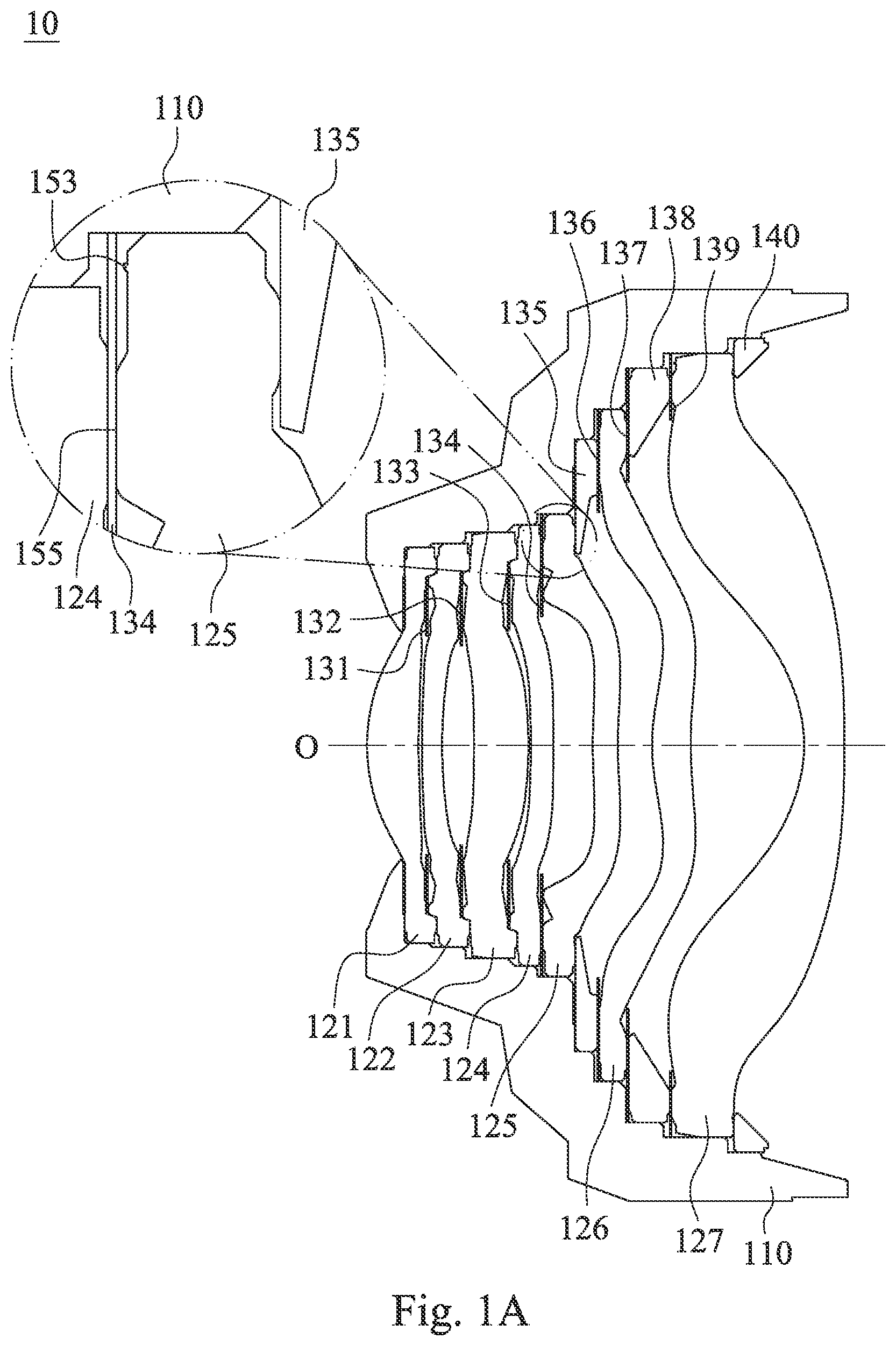
A is a schematic view of an imaging lens assembly 10 according to the 1st example of the present disclosure. In A , the imaging lens assembly 10 includes a plastic lens barrel 110 and an imaging lens element set (its reference numeral is omitted), wherein the imaging lens element set is accommodated in the plastic lens barrel 110 .
In particular, the imaging lens element set, in order from an object side to an image side, includes a lens element 121 , a light blocking element 131 , a lens element 122 , a light blocking element 132 , a lens element 123 , a light blocking element 133 , a lens element 124 , a light blocking element 134 , a lens element 125 , light blocking elements 135 , 136 , a lens element 126 , light blocking elements 137 , 138 , 139 , a lens element 127 and a retainer 140 , wherein the optical features such as structures, surface shapes and so on of the lens elements, the light blocking elements and the retainer can be disposed according to different imaging demand, and the optical features are not limited thereto.
B is a three dimensional view of the lens element 125 according to the 1st example in A . C is a schematic view of the lens element 125 according to the 1st example in A . D is a schematic view of parameters of the lens element 125 according to the 1st example in A . In A to 1 D , the lens element 125 has a central axis O, and includes an optical effective portion 151 , a peripheral portion 152 and a plurality of protruding structures 153 , wherein the central axis O passes through the optical effective portion 151 , and the peripheral portion 152 surrounds the optical effective portion 151 . The degree of fitting between the mold (not shown) and the lens element 125 can be enhanced during the molding process of the lens element 125 by disposing the protruding structures 153 , so that the warpage or the deformation can be prevented during the demolding process.
According to the 1st example, a number of the protruding structures 153 is twenty nine, but the number is not limited thereto.
In B and 1 D , the optical effective portion 151 includes a first optical surface 151 a and a second optical surface 151 b , wherein the second optical surface 151 b and the first optical surface 151 a are disposed relative to each other, and both of the first optical surface 151 a and the second optical surface 151 b are optical aspheric surfaces. Therefore, the lens element with high resolution can be provided.
The peripheral portion 152 surrounds the optical effective portion 151 , and includes a first peripheral surface 152 a , a second peripheral surface 152 b and an outer annular surface 152 c , wherein the first peripheral surface 152 a and the first optical surface 151 a face towards the same side, the second peripheral surface 152 b and the second optical surface 151 b face towards the same side, and the outer annular surface 152 c is connected to the first peripheral surface 152 a and the second peripheral surface 152 b.
In C , the protruding structures 153 are disposed on the first peripheral surface 152 a , the protruding structures 153 extend along a spiral path and are disposed at intervals, and the spiral path surrounds the optical effective portion 151 and is tapered towards the central axis O. The faster processing flow of the mold can be obtained by disposing the protruding structures 153 along a spiral path to enhance the efficiency of the process of mold. Also, the number and the distribution of the protruding structures 153 can be more conveniently adjusted according to the different design and molding conditions. Furthermore, the protruding structures 153 are gradually close along the spiral path towards the central axis O. Therefore, the aforementioned disposition is favorable for the automated process of the mold processing.
In particular, the spiral path can be tapered clockwise towards the center, or the spiral path can be tapered counterclockwise towards the center, wherein the spiral path can be Archimedean spiral, Fermat's spiral or Logarithmic spiral, but the present disclosure is not limited thereto. Further, the protruding structures 153 extend along the spiral path, which represents the protruding structures 153 extend from a first position on the spiral path to a second position on the spiral path. Further, the second position is closer to the central axis O than the first position to the central axis O.
In D , each of at least three of the protruding structures 153 has a first identification end 156 a and a second identification end 156 b on a cross section vertical to the first peripheral surface 152 a , wherein each of the first identification ends 156 a is connected to the first peripheral surface 152 a , and a spacing distance is between each of the second identification ends 156 b and the first peripheral surface 152 a . In particular, observing and identifying from a direction vertical to the first peripheral surface 152 a , the first identification end 156 a and the second identification end 156 b can be one end of each of the protruding structures 153 close to the optical effective portion 151 and the other end of each of the protruding structures 153 away from the optical effective portion 151 , respectively.
Moreover, each of the protruding structures 153 on the cross section vertical to the first peripheral surface 152 a further has a top 156 c , wherein the top 156 c is a highest point of each of the protruding structures 153 , and a spacing distance between the top 156 c and the second identification end 156 b along a direction vertical to the central axis O is less than a spacing distance between the top 156 c and the first identification end 156 a along the direction vertical to the central axis O. Therefore, the warpage or the deformation of the lens element 125 can be more effectively prevented.
In B to 1 D , the lens element 125 is formed by an injection molding, and the lens element 125 can further include at least one gate trace 154 , wherein the gate trace 154 is disposed on the outer annular surface 152 c . Therefore, the lens element with high precision and compact size can be provided.
In A and 1 D , the lens element 125 can further include a receiving surface 155 , wherein the receiving surface 155 and the first optical surface 151 a face towards the same side, the receiving surface 155 is closer to the optical effective portion 151 than the protruding structures 153 to the optical effective portion 151 , and the receiving surface 155 is against the light blocking element 134 . Therefore, the flatness of the receiving surface 155 can be ensured, so that the assembling tolerance can be reduced for providing the imaging lens assembly 10 with high resolution.
In C and 1 D , the first one of the protruding structures 153 on the spiral path is a first protruding structure 153 a , and the last one of the protruding structures 153 on the spiral path is a last protruding structure 153 b , and an angle is formed between a side of each of the protruding structures 153 at the second identification end 156 b and the first peripheral surface 152 a . When a distance between the first protruding structure 153 a and the central axis O is DS, a distance between the last protruding structure 153 b and the central axis O is DE, a central distance between the first optical surface 151 a and the first peripheral surface 152 a is t, a central distance between the first optical surface 151 a and the second optical surface 151 b is CT, a distance between the outer annular surface 152 c and the central axis O is ψ, a length of each of the protruding structures 153 along the spiral path is S1, a spacing distance between the protruding structures 153 along the spiral path is S2, and the angle is a, the following conditions of Table 1 are satisfied.
TABLE 1
1st example
DS (mm) 3.01 S2 (mm) 0.31
DE (mm) 2.843 α (degree) 60
t (mm) 0.639 DS-DE (mm) 0.167
CT (mm) 0.335 t/CT 1.907
ψ (mm) 3.094 DS/ψ 0.97
S1 (mm) 0.42 S1/S2 1.35
2nd Example
A is a three dimensional view of the lens element 220 according to the 2nd example of the present disclosure. B is a schematic view of the lens element 220 according to the 2nd example in A . C is a schematic view of parameters of the lens element 220 according to the 2nd example in A . In A to 2 C , the lens element 220 has a central axis O, and includes an optical effective portion 251 , a peripheral portion 252 and a plurality of protruding structures 253 , wherein the central axis O passes through the optical effective portion 251 , and the peripheral portion 252 surrounds the optical effective portion 251 . The degree of fitting between the mold (not shown) and the lens element 220 can be enhanced during the molding process of the lens element 220 by disposing the protruding structures 253 , so that the warpage or the deformation can be prevented during the demolding process.
According to the 2nd example, a number of the protruding structures 253 is sixty five, but the number is not limited thereto.
The optical effective portion 251 includes a first optical surface 251 a and a second optical surface 251 b , wherein the second optical surface 251 b and the first optical surface 251 a are disposed relative to each other, and both of the first optical surface 251 a and the second optical surface 251 b are optical aspheric surfaces. Therefore, the lens element with high resolution can be provided.
The peripheral portion 252 surrounds the optical effective portion 251 , and includes a first peripheral surface 252 a , a second peripheral surface 252 b and an outer annular surface 252 c , wherein the first peripheral surface 252 a and the first optical surface 251 a face towards the same side, the second peripheral surface 252 b and the second optical surface 251 b face towards the same side, and the outer annular surface 252 c is connected to the first peripheral surface 252 a and the second peripheral surface 252 b.
In B , the protruding structures 253 are disposed on the first peripheral surface 252 a , the protruding structures 253 extend along a spiral path and are disposed at intervals, the spiral path surrounds the optical effective portion 251 and is tapered towards the central axis O, and the protruding structures 253 are gradually close along the spiral path towards the central axis O.
In C , each of at least three of the protruding structures 253 has a first identification end 256 a and a second identification end 256 b on a cross section vertical to the first peripheral surface 252 a , wherein each of the first identification ends 256 a is connected to the first peripheral surface 252 a , and a spacing distance is between each of the second identification ends 256 b and the first peripheral surface 252 a . In particular, observing and identifying from a direction vertical to the first peripheral surface 252 a , the first identification end 256 a and the second identification end 256 b can be one end of each of the protruding structures 253 close to the optical effective portion 251 and the other end of each of the protruding structures 253 away from the optical effective portion 251 , respectively.
Moreover, each of the protruding structures 253 on the cross section vertical to the first peripheral surface 252 a further has a top 256 c , wherein the top 256 c is a highest point of each of the protruding structures 253 , and a spacing distance between the top 256 c and the second identification end 256 b along a direction vertical to the central axis O is less than a spacing distance between the top 256 c and the first identification end 256 a along the direction vertical to the central axis O. Therefore, the warpage or the deformation of the lens element 220 can be more effectively prevented.
In A to 2 C , the lens element 220 is formed by an injection molding, and the lens element 220 can further include at least one gate trace 254 , wherein the gate trace 254 is disposed on the outer annular surface 252 c . Therefore, the lens element with high precision and compact size can be provided.
In B and 20 , the first one of the protruding structures 253 on the spiral path is a first protruding structure 253 a , and the last one of the protruding structures 253 on the spiral path is a last protruding structure 253 b , and an angle is formed between a side of each of the protruding structures 253 at the second identification end 256 b and the first peripheral surface 252 a . When a distance between the first protruding structure 253 a and the central axis O is DS, a distance between the last protruding structure 253 b and the central axis O is DE, a central distance between the first optical surface 251 a and the first peripheral surface 252 a is t, a central distance between the first optical surface 251 a and the second optical surface 251 b is CT, a distance between the outer annular surface 252 c and the central axis O is ψ, a length of each of the protruding structures 253 along the spiral path is S1, a spacing distance between the protruding structures 253 along the spiral path is S2, and the angle is a, the following conditions of Table 2 are satisfied.
TABLE 2
2nd example
DS (mm) 3.015 S2 (mm) 0.48
DE (mm) 2.815 α (degree) 70
t (mm) 0.639 DS-DE (mm) 0.2
CT (mm) 0.335 t/CT 1.907
ψ (mm) 3.094 DS/ψ 0.97
S1 (mm) 0.26 S1/S2 0.54
Further, all of other structures and dispositions according to the 2nd example are the same as the structures and the dispositions according to the 1st example, and will not be described again herein.
3rd Example
A is a three dimensional view of the lens element 320 according to the 3rd example of the present disclosure. B is a schematic view of the lens element 320 according to the 3rd example in A . C is a schematic view of parameters of the lens element 320 according to the 3rd example in A . In A to 3 C , the lens element 320 has a central axis O, and includes an optical effective portion 351 , a peripheral portion 352 and a plurality of protruding structures 353 , wherein the central axis O passes through the optical effective portion 351 , and the peripheral portion 352 surrounds the optical effective portion 351 . The degree of fitting between the mold (not shown) and the lens element 320 can be enhanced during the molding process of the lens element 320 by disposing the protruding structures 353 , so that the warpage or the deformation can be prevented during the demolding process.
According to the 3rd example, a number of the protruding structures 353 is twenty two, but the number is not limited thereto.
The optical effective portion 351 includes a first optical surface 351 a and a second optical surface 351 b , wherein the second optical surface 351 b and the first optical surface 351 a are disposed relative to each other, and both of the first optical surface 351 a and the second optical surface 351 b are optical aspheric surfaces. Therefore, the lens element with high resolution can be provided.
The peripheral portion 352 surrounds the optical effective portion 351 , and includes a first peripheral surface 352 a , a second peripheral surface 352 b and an outer annular surface 352 c , wherein the first peripheral surface 352 a and the first optical surface 351 a face towards the same side, the second peripheral surface 352 b and the second optical surface 351 b face towards the same side, and the outer annular surface 352 c is connected to the first peripheral surface 352 a and the second peripheral surface 352 b.
In B , the protruding structures 353 are disposed on the first peripheral surface 352 a , the protruding structures 353 extend along a spiral path and are disposed at intervals, the spiral path surrounds the optical effective portion 351 and is tapered towards the central axis O, and the protruding structures 353 are gradually close along the spiral path towards the central axis O.
In C , each of at least three of the protruding structures 353 has a first identification end 356 a and a second identification end 356 b on a cross section vertical to the first peripheral surface 352 a , wherein each of the first identification ends 356 a is connected to the first peripheral surface 352 a , and a spacing distance is between each of the second identification ends 356 b and the first peripheral surface 352 a . In particular, observing and identifying from a direction vertical to the first peripheral surface 352 a , the first identification end 356 a and the second identification end 356 b can be one end of each of the protruding structures 353 close to the optical effective portion 351 and the other end of each of the protruding structures 353 away from the optical effective portion 351 , respectively.
Moreover, each of the protruding structures 353 on the cross section vertical to the first peripheral surface 352 a further has a top 356 c , wherein the top 356 c is a highest point of each of the protruding structures 353 , and a spacing distance between the top 356 c and the second identification end 356 b along a direction vertical to the central axis O is less than a spacing distance between the top 356 c and the first identification end 356 a along the direction vertical to the central axis O. Therefore, the warpage or the deformation of the lens element 320 can be more effectively prevented.
In A to 3 C , the lens element 320 is formed by an injection molding, and the lens element 320 can further include at least one gate trace 354 , wherein the gate trace 354 is disposed on the outer annular surface 352 c . Therefore, the lens element with high precision and compact size can be provided.
In B and 3 C , the first one of the protruding structures 353 on the spiral path is a first protruding structure 353 a , and the last one of the protruding structures 353 on the spiral path is a last protruding structure 353 b , and an angle is formed between a side of each of the protruding structures 353 at the second identification end 356 b and the first peripheral surface 352 a . When a distance between the first protruding structure 353 a and the central axis O is DS, a distance between the last protruding structure 353 b and the central axis O is DE, a central distance between the first optical surface 351 a and the first peripheral surface 352 a is t, a central distance between the first optical surface 351 a and the second optical surface 351 b is CT, a distance between the outer annular surface 352 c and the central axis O is ψ, a length of each of the protruding structures 353 along the spiral path is S1, a spacing distance between the protruding structures 353 along the spiral path is S2, and the angle is a, the following conditions of Table 3 are satisfied.
TABLE 3
3rd example
DS (mm) 3.01 S2 (mm) 0.31
DE (mm) 2.948 α (degree) 87
t (mm) 0.639 DS-DE (mm) 0.062
CT (mm) 0.335 t/CT 1.907
ψ (mm) 3.094 DS/ψ 0.97
S1 (mm) 1.00 S1/S2 3.23
Further, all of other structures and dispositions according to the 3rd example are the same as the structures and the dispositions according to the 1st example, and will not be described again herein.
4th Example
A is a schematic view of the lens element 420 according to the 4th example of the present disclosure. B is a schematic view of parameters of the lens element 420 according to the 4th example in A . In A and 4 B , the lens element 420 has a central axis O, and includes an optical effective portion 451 , a peripheral portion 452 and a plurality of protruding structures 453 , wherein the central axis O passes through the optical effective portion 451 , and the peripheral portion 452 surrounds the optical effective portion 451 . The degree of fitting between the mold (not shown) and the lens element 420 can be enhanced during the molding process of the lens element 420 by disposing the protruding structures 453 , so that the warpage or the deformation can be prevented during the demolding process.
According to the 4th example, a number of the protruding structures 453 is twenty four, but the number is not limited thereto.
The optical effective portion 451 includes a first optical surface 451 a and a second optical surface 451 b , wherein the second optical surface 451 b and the first optical surface 451 a are disposed relative to each other. Therefore, the lens element with high resolution can be provided.
The peripheral portion 452 surrounds the optical effective portion 451 , and includes a first peripheral surface 452 a , a second peripheral surface 452 b and an outer annular surface 452 c , wherein the first peripheral surface 452 a and the first optical surface 451 a face towards the same side, the second peripheral surface 452 b and the second optical surface 451 b face towards the same side, and the outer annular surface 452 c is connected to the first peripheral surface 452 a and the second peripheral surface 452 b.
In A , the protruding structures 453 are disposed on the first peripheral surface 452 a , the protruding structures 453 extend along a spiral path and are disposed at intervals, the spiral path surrounds the optical effective portion 451 and is tapered towards the central axis O, and the protruding structures 453 are gradually close along the spiral path towards the central axis O.
In B , each of at least three of the protruding structures 453 has a first identification end 456 a and a second identification end 456 b on a cross section vertical to the first peripheral surface 452 a , wherein each of the first identification ends 456 a is connected to the first peripheral surface 452 a , and a spacing distance is between each of the second identification ends 456 b and the first peripheral surface 452 a . In particular, observing and identifying from a direction vertical to the first peripheral surface 452 a , the first identification end 456 a and the second identification end 456 b can be one end of each of the protruding structures 453 close to the optical effective portion 451 and the other end of each of the protruding structures 453 away from the optical effective portion 451 , respectively.
Moreover, each of the protruding structures 453 on the cross section vertical to the first peripheral surface 452 a further has a top 456 c , wherein the top 456 c is a highest point of each of the protruding structures 453 , and a spacing distance between the top 456 c and the second identification end 456 b along a direction vertical to the central axis O is less than a spacing distance between the top 456 c and the first identification end 456 a along the direction vertical to the central axis O. Therefore, the warpage or the deformation of the lens element 420 can be more effectively prevented.
In A and 4 B , the lens element 420 is formed by an injection molding, and the lens element 420 can further include at least one gate trace 454 , wherein the gate trace 454 is disposed on the outer annular surface 452 c . Therefore, the lens element with high precision and compact size can be provided.
The first one of the protruding structures 453 on the spiral path is a first protruding structure 453 a , and the last one of the protruding structures 453 on the spiral path is a last protruding structure 453 b , and an angle is formed between a side of each of the protruding structures 453 at the second identification end 456 b and the first peripheral surface 452 a . When a distance between the first protruding structure 453 a and the central axis O is DS, a distance between the last protruding structure 453 b and the central axis O is DE, a central distance between the first optical surface 451 a and the first peripheral surface 452 a is t, a central distance between the first optical surface 451 a and the second optical surface 451 b is CT, a distance between the outer annular surface 452 c and the central axis O is ψ, a length of each of the protruding structures 453 along the spiral path is S1, a spacing distance between the protruding structures 453 along the spiral path is S2, and the angle is a, the following conditions of Table 4 are satisfied.
TABLE 4
4th example
DS (mm) 4.422 S2 (mm) 0.94
DE (mm) 4.35 α (degree) 70
t (mm) 0.69 DS-DE (mm) 0.072
CT (mm) 0.516 t/CT 1.337
ψ (mm) 4.5 DS/ψ 0.98
S1 (mm) 0.54 S1/S2 0.57
Further, all of other structures and dispositions according to the 4th example are the same as the structures and the dispositions according to the 1st example, and will not be described again herein.
5th Example
A is a schematic view of the lens element 520 according to the 5th example of the present disclosure. B is a schematic view of parameters of the lens element 520 according to the 5th example in A . In A and 5 B , the lens element 520 has a central axis O, and includes an optical effective portion 551 , a peripheral portion 552 and a plurality of protruding structures 553 , wherein the central axis O passes through the optical effective portion 551 , and the peripheral portion 552 surrounds the optical effective portion 551 . The degree of fitting between the mold (not shown) and the lens element 520 can be enhanced during the molding process of the lens element 520 by disposing the protruding structures 553 , so that the warpage or the deformation can be prevented during the demolding process.
According to the 5th example, a number of the protruding structures 553 is thirteen, but the number is not limited thereto.
The optical effective portion 551 includes a first optical surface 551 a and a second optical surface 551 b , wherein the second optical surface 551 b and the first optical surface 551 a are disposed relative to each other. Therefore, the lens element with high resolution can be provided.
The peripheral portion 552 surrounds the optical effective portion 551 , and includes a first peripheral surface 552 a , a second peripheral surface 552 b and an outer annular surface 552 c , wherein the first peripheral surface 552 a and the first optical surface 551 a face towards the same side, the second peripheral surface 552 b and the second optical surface 551 b face towards the same side, and the outer annular surface 552 c is connected to the first peripheral surface 552 a and the second peripheral surface 552 b.
In A , the protruding structures 553 are disposed on the first peripheral surface 552 a , the protruding structures 553 extend along a spiral path and are disposed at intervals, the spiral path surrounds the optical effective portion 551 and is tapered towards the central axis O, and the protruding structures 553 are gradually close along the spiral path towards the central axis O.
In B , each of at least three of the protruding structures 553 has a first identification end 556 a and a second identification end 556 b on a cross section vertical to the first peripheral surface 552 a , wherein each of the first identification ends 556 a is connected to the first peripheral surface 552 a , and a spacing distance is between each of the second identification ends 556 b and the first peripheral surface 552 a . In particular, observing and identifying from a direction vertical to the first peripheral surface 552 a , the first identification end 556 a and the second identification end 556 b can be one end of each of the protruding structures 553 away from the optical effective portion 551 and the other end of each of the protruding structures 553 close to the optical effective portion 551 , respectively.
Moreover, each of the protruding structures 553 on the cross section vertical to the first peripheral surface 552 a further has a top 556 c , wherein the top 556 c is a highest point of each of the protruding structures 553 , and a spacing distance between the top 556 c and the second identification end 556 b along a direction vertical to the central axis O is less than a spacing distance between the top 556 c and the first identification end 556 a along the direction vertical to the central axis O. Therefore, the warpage or the deformation of the lens element 520 can be more effectively prevented.
In A and 5 B , the lens element 520 is formed by an injection molding, and the lens element 520 can further include at least one gate trace 554 , wherein the gate trace 554 is disposed on the outer annular surface 552 c . Therefore, the lens element with high precision and compact size can be provided.
The first one of the protruding structures 553 on the spiral path is a first protruding structure 553 a , and the last one of the protruding structures 553 on the spiral path is a last protruding structure 553 b , and an angle is formed between a side of each of the protruding structures 553 at the second identification end 556 b and the first peripheral surface 552 a . When a distance between the first protruding structure 553 a and the central axis O is DS, a distance between the last protruding structure 553 b and the central axis O is DE, a central distance between the first optical surface 551 a and the first peripheral surface 552 a is t, a central distance between the first optical surface 551 a and the second optical surface 551 b is CT, a distance between the outer annular surface 552 c and the central axis O is ψ, a length of each of the protruding structures 553 along the spiral path is S1, a spacing distance between the protruding structures 553 along the spiral path is S2, and the angle is α, the following conditions of Table 5 are satisfied.
TABLE 5
5th example
DS (mm) 5.129 S2 (mm) 0.92
DE (mm) 5.079 α (degree) 78
t (mm) 1.715 DS-DE (mm) 0.05
CT (mm) 0.54 t/CT 3.176
ψ (mm) 5.245 DS/ψ 0.98
S1 (mm) 1.58 S1/S2 1.72
Further, all of other structures and dispositions according to the 5th example are the same as the structures and the dispositions according to the 1st example, and will not be described again herein.
6th Example
A is a schematic view of an electronic device 60 according to the 6th example of the present disclosure. B is another schematic view of the electronic device 60 according to the 6th example in A . In A and 6 B , the electronic device 60 is a smart phone, and includes a camera module (its reference numeral is omitted) and a user interface 61 , wherein the camera module includes an imaging lens assembly (not shown) and an image sensor (not shown), and the image sensor is disposed on an image surface (not shown) of the imaging lens assembly. Moreover, the camera module can be an ultra-wide angle camera module 62 , a high resolution camera module 63 and a telephoto camera module 64 , and the user interface 61 is a touch screen, but the present disclosure is not limited thereto.
Moreover, the imaging lens assembly includes a plastic lens barrel (not shown) and an imaging lens element set (not shown), wherein the imaging lens element set can be accommodated in the plastic lens barrel, and the imaging lens element set includes at least one lens element (not shown). In particular, the lens element can be one of the lens elements according to the aforementioned 1st example to the 5th example, but the present disclosure is not limited thereto.
Users enter a shooting mode via the user interface 61 , wherein the user interface 61 is configured to display the scene, and the shooting angle can be manually adjusted to switch the ultra-wide angle camera module 62 , the high resolution camera module 63 and the telephoto camera module 64 . At this moment, the imaging light is gathered on the image sensor via the camera module, and an electronic signal about an image is output to an image signal processor (ISP) 65 .
In B , to meet a specification of the electronic device 60 , the electronic device 60 can further include an optical anti-shake mechanism (not shown). Furthermore, the electronic device 60 can further include at least one focusing assisting module (its reference numeral is omitted) and at least one sensing element (not shown). The focusing assisting module can be a flash module 66 for compensating a color temperature, an infrared distance measurement component, a laser focus module and so on. The sensing element can have functions for sensing physical momentum and kinetic energy, such as an accelerator, a gyroscope, a Hall Effect Element, to sense shaking or jitters applied by hands of the users or external environments. Accordingly, the camera module of the electronic device 60 equipped with an auto-focusing mechanism and the optical anti-shake mechanism can be enhanced to achieve the superior image quality. Furthermore, the electronic device 60 according to the present disclosure can have a capturing function with multiple modes, such as taking optimized selfies, high dynamic range (HDR) under a low light condition, 4K resolution recording and so on. Furthermore, the users can visually see a captured image of the camera through the user interface 61 and manually operate the view finding range on the user interface 61 to achieve the autofocus function of what you see is what you get.
Moreover, the camera module, the image sensor, the optical anti-shake mechanism, the sensing element and the focusing assisting module can be disposed on a flexible printed circuit board (FPC) (not shown) and electrically connected to the associated components, such as the image signal processor 65 , via a connector (not shown) to perform a capturing process. Since the current electronic devices, such as smart phones, have a tendency of being compact, the way of firstly disposing the camera module and related components on the flexible printed circuit board and secondly integrating the circuit thereof into the main board of the electronic device via the connector can satisfy the requirements of the mechanical design and the circuit layout of the limited space inside the electronic device, and obtain more margins. The autofocus function of the camera module can also be controlled more flexibly via the touch screen of the electronic device. According to the 6th example, the electronic device 60 can include a plurality of sensing elements and a plurality of focusing assisting modules. The sensing elements and the focusing assisting modules are disposed on the flexible printed circuit board and at least one other flexible printed circuit board (not shown) and electrically connected to the associated components, such as the image signal processor 65 , via corresponding connectors to perform the capturing process. In other examples (not shown herein), the sensing elements and the focusing assisting modules can also be disposed on the main board of the electronic device or carrier boards of other types according to requirements of the mechanical design and the circuit layout.
Furthermore, the electronic device 60 can further include, but not be limited to, a display, a control unit, a storage unit, a random access memory (RAM), a read-only memory (ROM), or the combination thereof.
C is a schematic view of an image captured via the electronic device 60 according to the 6th example in A . In C , the larger range of the image can be captured via the ultra-wide angle camera module 62 , and the ultra-wide angle camera module 62 has the function of accommodating wider range of the scene.
D is another schematic view of an image captured via the electronic device 60 according to the 6th example in A . In D , the image of the certain range with the high resolution can be captured via the high resolution camera module 63 , and the high resolution camera module 63 has the function of the high resolution and the low deformation.
E is still another schematic view of an image captured via the electronic device 60 according to the 6th example in A . In E , the telephoto camera module 64 has the enlarging function of the high magnification, and the distant image can be captured and enlarged with high magnification via the telephoto camera module 64 .
In C to 6 E , the zooming function can be obtained via the electronic device 60 , when the scene is captured via the camera module with different focal lengths cooperated with the function of image processing.
7th Example
is a schematic view of an electronic device 70 according to the 7th example of the present disclosure. In , the electronic device 70 is a smart phone, and includes a camera module (its reference numeral is omitted), wherein the camera module includes an imaging lens assembly (not shown) and an image sensor (not shown), and the image sensor is disposed on an image surface (not shown) of the imaging lens assembly. Moreover, the camera module can be ultra-wide angle camera modules 711 , 712 , wide angle camera modules 713 , 714 , telephoto camera modules 715 , 716 , 717 , 718 and a Time-Of-Flight (TOF) module 719 . The TOF module 719 can be another type of the camera module, and the disposition is not limited thereto.
Moreover, the imaging lens assembly includes a plastic lens barrel (not shown) and an imaging lens element set (not shown), wherein the imaging lens element set can be accommodated in the plastic lens barrel, and the imaging lens element set includes at least one lens element (not shown). In particular, the lens element can be one of the lens elements according to the aforementioned 1st example to the 5th example, but the present disclosure is not limited thereto.
Further, the telephoto camera modules 717 , 718 are configured to fold the light, but the present disclosure is not limited thereto.
To meet a specification of the electronic device 70 , the electronic device 70 can further include an optical anti-shake mechanism (not shown). Furthermore, the electronic device 70 can further include at least one focusing assisting module (not shown) and at least one sensing element (not shown). The focusing assisting module can be a flash module 720 for compensating a color temperature, an infrared distance measurement component, a laser focus module and so on. The sensing element can have functions for sensing physical momentum and kinetic energy, such as an accelerator, a gyroscope, a Hall Effect Element, to sense shaking or jitters applied by hands of the users or external environments. Accordingly, the camera module of the electronic device 70 equipped with an auto-focusing mechanism and the optical anti-shake mechanism can be enhanced to achieve the superior image quality. Furthermore, the electronic device 70 according to the present disclosure can have a capturing function with multiple modes, such as taking optimized selfies, High Dynamic Range (HDR) under a low light condition, 4K Resolution recording and so on.
Further, all of other structures and dispositions according to the 7th example are the same as the structures and the dispositions according to the 6th example, and will not be described again herein.
8th Example
A is a schematic view of a vehicle instrument 80 according to the 8th example of the present disclosure. B is another schematic view of the vehicle instrument 80 according to the 8th example in A . C is still another schematic view of the vehicle instrument 80 according to the 8th example in A . In A to 8 C , the vehicle instrument 80 includes a plurality of camera modules 81 , and each of the camera modules 81 includes an imaging lens assembly (not shown) and an image sensor (not shown), and the image sensor is disposed on an image surface (not shown) of the imaging lens assembly. According to the 8th example, a number of the camera modules 81 is six, but the present disclosure is not limited thereto.
Moreover, the imaging lens assembly includes a plastic lens barrel (not shown) and an imaging lens element set (not shown), wherein the imaging lens element set can be accommodated in the plastic lens barrel, and the imaging lens element set includes at least one lens element (not shown). In particular, the lens element can be one of the lens elements according to the aforementioned 1st example to the 5th example, but the present disclosure is not limited thereto.
In A and 8 B , the camera modules 81 are automotive camera modules, two of the camera modules 81 are located under rearview mirrors on a left side and a right side, respectively, and the aforementioned camera modules 81 are configured to capture the image information of a visual angle θ. In particular, the visual angle θ can satisfy the following condition: 40 degrees<θ<90 degrees. Therefore, the image information in the regions of two lanes on the left side and the right side can be captured.
In B , another two of the camera modules 81 can be disposed in the inner space of the vehicle instrument 80 . In particular, the aforementioned two camera modules 81 are disposed on a location close to the rearview mirror inside the vehicle instrument 80 and a location close to the rear car window, respectively. Moreover, the camera modules 81 can be further disposed on the rearview mirrors on the left side and the right side except the mirror surface, respectively, but the present disclosure is not limited thereto.
In C , another two of the camera modules 81 can be disposed on a front end of the vehicle instrument 80 and a rear end of the vehicle instrument 80 , respectively. By disposing the camera modules 81 on the front end and the rear end of the vehicle instrument 80 and under the rearview mirror on the left side of the vehicle instrument 80 and the right side of the vehicle instrument 80 , it is favorable for the drivers obtaining the external space information in addition to the driving seat, such as the external space informations I 1 , I 2 , I 3 , I 4 , but the present disclosure is not limited thereto. Therefore, more visual angles can be provided to reduce the blind spot, so that the driving safety can be improved.
The foregoing description, for purpose of explanation, has been described with reference to specific examples. It is to be noted that Tables show different data of the different examples; however, the data of the different examples are obtained from experiments. The examples were chosen and described in order to best explain the principles of the disclosure and its practical applications, to thereby enable others skilled in the art to best utilize the disclosure and various examples with various modifications as are suited to the particular use contemplated. The examples depicted above and the appended drawings are exemplary and are not intended to be exhaustive or to limit the scope of the present disclosure to the precise forms disclosed. Many modifications and variations are possible in view of the above teachings.
Figures (20)
Citations
This patent cites (14)
- US7830610
- US9798048
- US9946047
- US10001624
- US10018808
- US10114152
- US10317648
- US10436952
- US10502873
- US10527756
- US10656392
- US10928554
- US11156795
- US2011/0090582