Color Conversion Substrate and Display Device
Abstract
A color conversion substrate includes: a bank having a first open region and a second open region; a color conversion layer in the first opening region, the color conversion layer including color conversion particles; a first partition wall partitioning the second opening region into a central region and a peripheral region surrounding the central region, the first partition wall having a polygonal shape with n vertices in a plan view where n is a natural number greater than or equal to 3; and n second partition walls extending from the n vertices of the first partition wall to an edge of the second opening region, respectively, to partition the peripheral region into n sub-regions.
Claims (22)
1. A color conversion substrate comprising: a bank having a plurality of first opening regions and a second opening region; a color conversion layer in the first opening regions, the color conversion layer comprising color conversion particles; a first partition wall partitioning the second opening region into a central region and a peripheral region surrounding the central region, the first partition wall having a polygonal shape with n vertices in a plan view where n is a natural number greater than or equal to 3; and n second partition walls extending from the n vertices of the first partition wall to an edge of the second opening region, respectively, to partition the peripheral region into n sub-regions, wherein the central region is located between adjacent first opening regions of the plurality of first opening regions and does not overlap the color conversion layer.
16. A display device comprising: a color conversion substrate comprising: a bank having a first opening region and a second opening region; a color conversion layer in the first opening region, the color conversion layer comprising color conversion particles; a first partition wall partitioning the second opening region into a central region and a peripheral region surrounding the central region, the first partition wall having a polygonal shape with n vertices in a plan view where n is a natural number greater than or equal to 3; and n second partition walls extending from the n vertices of the first partition wall to an edge of the second opening region, respectively, to partition the peripheral region into n sub-regions; and an array substrate overlapping the color conversion substrate, the array substrate comprising a plurality of light emitting elements, a light emitting element of the plurality of light emitting elements overlapping the first opening region, wherein the central region is located in a light blocking area between adjacent light emitting elements of the plurality of light emitting elements.
Show 20 dependent claims
2. The color conversion substrate of claim 1 , wherein each of the n second partition walls is perpendicular to the edge of the second opening region.
3. The color conversion substrate of claim 1 , wherein a first thickness of the first partition wall is different from a second thickness of each of the n second partition walls.
4. The color conversion substrate of claim 1 , wherein a first thickness of the first partition wall is 5 μm or more and 25 μm or less, and wherein a second thickness of each of the n second partition walls is 5 μm or more and 25 μm or less.
5. The color conversion substrate of claim 1 , wherein an area of each of the n sub-regions is smaller than an area of the central region.
6. The color conversion substrate of claim 1 , wherein an angle between a second partition wall of the n second partition walls and the first partition wall contacting the second partition wall is greater than or equal to 90 degrees.
7. The color conversion substrate of claim 1 , further comprising a light blocking layer overlapping the second opening region.
8. The color conversion substrate of claim 1 , wherein the first partition wall has an octagonal shape comprising a first side, a second side contacting the first side, a third side contacting the second side, a fourth side contacting the third side, a fifth side contacting the fourth side, a sixth side contacting the fifth side, a seventh side contacting the sixth side, and an eighth side contacting the first side and the seventh side in the plan view, and wherein the n second partition walls comprise a first compartmental wall contacting the first side and the second side, a second compartmental wall contacting the second side and the third side, a third compartmental wall contacting the third side and the fourth side, a fourth compartmental wall contacting the fourth side and the fifth side, a fifth compartmental wall contacting the fifth side and the sixth side, a sixth compartmental wall contacting the sixth side and the seventh side, a seventh compartmental wall contacting the seventh side and the eighth side, and an eighth compartmental wall contacting the eighth side and the first side.
9. The color conversion substrate of claim 8 , wherein the first side and the fifth side extend in a first direction, and wherein the third side and the seventh side extend in a second direction that is perpendicular to the first direction.
10. The color conversion substrate of claim 8 , wherein each of the first compartmental wall and the eighth compartmental wall is perpendicular to the first side, wherein each of the second compartmental wall and the third compartmental wall is perpendicular to the third side, wherein each of the fourth compartmental wall and the fifth compartmental wall is perpendicular to the fifth side, and wherein each of the sixth compartmental wall and the seventh compartmental wall is perpendicular to the seventh side.
11. The color conversion substrate of claim 8 , wherein each of the first to eighth compartmental walls has a first length, wherein each of the first side, the third side, the fifth side, and the seventh side has a second length that is different from the first length, and wherein each of the second side, the fourth side, the sixth side, and the eighth side has a third length that is different from the first length and the second length.
12. The color conversion substrate of claim 11 , wherein the first length is smaller than the second length, and wherein the first length is smaller than the third length.
13. The color conversion substrate of claim 1 , wherein the first partition wall comprises a first side, a second side contacting the first side, a third side contacting the second side, a fourth side contacting the third side, a fifth side contacting the fourth side, and a sixth side contacting the fifth side and the first side, and wherein the n second partition walls comprise a first compartmental wall contacting the first side and the second side, a second compartmental wall contacting the second side and the third side, a third compartmental wall contacting the third side and the fourth side, a fourth compartmental wall contacting the fourth side and the fifth side, a fifth compartmental wall contacting the fifth side and the sixth side, and a sixth compartmental wall contacting the sixth side and the first side.
14. The color conversion substrate of claim 13 , wherein the first side and the fourth side are parallel to each other, wherein the second side and the fifth side are parallel to each other, and wherein the third side and the sixth side are parallel to each other.
15. The color conversion substrate of claim 13 , wherein each of the first compartmental wall and the sixth compartmental wall is perpendicular to the first side, and wherein each of the third compartmental wall and the fourth compartmental wall is perpendicular to the fourth side.
17. The display device of claim 16 , wherein the array substrate comprises: a first light emitting element row comprising a first light emitting element and a second light emitting element, the first light emitting element and the second light emitting element being alternately arranged in a first direction; and a second light emitting element row comprising third light emitting elements arranged in the first direction, the second light emitting element row being spaced from the first light emitting element row in a second direction that is perpendicular to the first direction, and wherein the first light emitting element row and the second light emitting element row are alternately arranged in the second direction.
18. The display device of claim 17 , wherein the first opening region comprises: a first color conversion region overlapping the first light emitting element; a second color conversion region overlapping the second light emitting element; and a third color conversion region overlapping a third light emitting element of the third light emitting elements, wherein the color conversion substrate comprises: a first color conversion row comprising the first color conversion region and the second color conversion region, the first color conversion region and the second color conversion region being alternately arranged in the first direction; and a second color conversion row comprising the third color conversion region and the second opening region, the third color conversion region and the second opening region being alternately arranged in the first direction, and wherein the first color conversion row and the second color conversion row are alternately arranged in the second direction.
19. The display device of claim 18 , wherein each of the first color conversion region, the second color conversion region, and the third color conversion region has a rectangular shape having a first area in the plan view, and wherein the second opening region has a rectangular shape having a second area that is larger than the first area in the plan view.
20. The display device of claim 18 , wherein the color conversion substrate further comprises: a third opening region located between the first color conversion region and the second color conversion region, the first color conversion region and the second color conversion region being adjacent to each other; and a fourth opening region located between the third color conversion region and the first color conversion row.
21. The display device of claim 20 , wherein a width of the third opening region in the first direction is smaller than a width of the first color conversion region in the first direction.
22. The display device of claim 20 , wherein a width of the fourth opening region in the second direction is smaller than a width of the third color conversion region in the second direction.
Full Description
Show full text →
CROSS-REFERENCE TO RELATED APPLICATION
This application claims priority to and the benefit of Korean Patent Application No. 10-2021-0059233 filed on May 7, 2021 in the Korean Intellectual Property Office (KIPO), the entire content of which is incorporated by reference herein.
BACKGROUND
1. Field
The present disclosure relates to a display device. More particularly, the present disclosure relates to a display device including a color conversion substrate.
2. Description of the Related Art
A display device may include a color conversion substrate and an array substrate overlapping the color conversion substrate. The color conversion substrate may include a bank including a first opening region and a color conversion layer disposed in the first opening region. The array substrate may include a light emitting element. The light emitting element may overlap the color conversion layer, and light emitted from the light emitting element may pass through the color conversion layer to have a specific color. The color conversion layer may be formed by an inkjet scheme.
The above information disclosed in this Background section is for enhancement of understanding of the background of the present disclosure, and therefore, it may contain information that does not constitute prior art
SUMMARY
Aspects of one or more embodiments of the present disclosure are directed toward a color conversion substrate capable of reducing a size of protrusion caused by erroneous jetting of an ink, and/or preventing the protrusion from being generated.
Aspects of one or more embodiments of the present disclosure are directed toward a display device capable of reducing damage to an array substrate caused by the protrusion.
However, aspects and features of the present disclosure are not limited to the above-described aspects and features, and may be variously expanded in a suitable manner without departing from the spirit and scope of the present disclosure.
According to one or more embodiments of the present disclosure, a color conversion substrate includes: a bank having a first open region and a second open region; a color conversion layer in the first opening region, the color conversion layer including color conversion particles; a first partition wall partitioning the second opening region into a central region and a peripheral region surrounding the central region, the first partition wall having a polygonal shape with n vertices in a plan view where n is a natural number greater than or equal to 3; and n second partition walls extending from the n vertices of the first partition wall to an edge of the second opening region, respectively, to partition the peripheral region into n sub-regions.
According to one or more embodiments, each of the n second partition walls may be perpendicular to the edge of the second opening region.
According to one or more embodiments, a first thickness of the first partition wall may be different from a second thickness of each of the n second partition walls.
According to one or more embodiments, a first thickness of the first partition wall may be 5 μm or more and 25 μm or less. A second thickness of each of the n second partition walls may be 5 μm or more and 25 μm or less.
According to one or more embodiments, an area of each of the n sub-regions may be smaller than an area of the central region.
According to one or more embodiments, an angle between a second partition wall of the n second partition walls and the first partition wall contacting (i.e., making contact with) the second partition wall may be greater than or equal to 90 degrees.
According to one or more embodiments, the color conversion substrate may further include a light blocking layer overlapping the second opening region.
According to one or more embodiments, the first partition wall may have an octagonal shape including a first side, a second side contacting the first side, a third side contacting the second side, a fourth side contacting the third side, a fifth side contacting the fourth side, a sixth side contacting the fifth side, a seventh side contacting the sixth side, and an eighth side contacting the first side and the seventh side in a plan view. The n second partition walls may include a first compartmental wall contacting the first side and the second side, a second compartmental wall contacting the second side and the third side, a third compartmental wall contacting the third side and the fourth side, a fourth compartmental wall contacting the fourth side and the fifth side, a fifth compartmental wall contacting the fifth side and the sixth side, a sixth compartmental wall contacting the sixth side and the seventh side, a seventh compartmental wall contacting the seventh side and the eighth side, and an eighth compartmental wall contacting the eighth side and the first side.
According to one or more embodiments, the first side and the fifth side may extend in a first direction. The third side and the seventh side may extend in a second direction that is perpendicular to the first direction.
According to one or more embodiments, each of the first compartmental wall and the eighth compartmental wall may be perpendicular to the first side. Each of the second compartmental wall and the third compartmental wall may be perpendicular to the third side. Each of the fourth compartmental wall and the fifth compartmental wall may be perpendicular to the fifth side. Each of the sixth compartmental wall and the seventh compartmental wall may be perpendicular to the seventh side.
According to one or more embodiments, each of the first to eighth compartmental walls may have a first length. Each of the first side, the third side, the fifth side, and the seventh side may have a second length that is different from the first length. Each of the second side, the fourth side, the sixth side, and the eighth side may have a third length that is different from the first length and the second length.
According to one or more embodiments, the first length may be smaller (e.g., shorter) than the second length. The first length may be smaller (e.g., shorter) than the third length.
According to one or more embodiments, the first partition wall may include a first side, a second side contacting the first side, a third side contacting the second side, a fourth side contacting the third side, a fifth side contacting the fourth side, and a sixth side contacting the fifth side and the first side. The n second partition walls may include a first compartmental wall contacting the first side and the second side, a second compartmental wall contacting the second side and the third side, a third compartmental wall contacting the third side and the fourth side, a fourth compartmental wall contacting the fourth side and the fifth side, a fifth compartmental wall contacting the fifth side and the sixth side, and a sixth compartmental wall contacting the sixth side and the first side.
According to one or more embodiments, the first side and the fourth side may be parallel to each other. The second side and the fifth side may be parallel to each other. The third side and the sixth side may be parallel to each other.
According to one or more embodiments, each of the first compartmental wall and the sixth compartmental wall may be perpendicular to the first side. Each of the third compartmental wall and the fourth compartmental wall may be perpendicular to the fourth side.
According to one or more embodiments of the present disclosure, a display device includes: a color conversion substrate including a bank having a first open region and a second open region; a color conversion layer in the first opening region, the color conversion layer including color conversion particles; a first partition wall partitioning the second opening region into a central region and a peripheral region surrounding the central region, the first partition wall having a polygonal shape with n vertices in a plan view where n is a natural number greater than or equal to 3; and n second partition walls extending from the n vertices of the first partition wall to an edge of the second opening region, respectively, to partition the peripheral region into n sub-regions; and an array substrate overlapping the color conversion substrate, the array substrate including a light emitting element overlapping the first opening region.
According to one or more embodiments, the array substrate may include: a first light emitting element row including a first light emitting element and a second light emitting element, the first light emitting element and the second light emitting element being alternately arranged in a first direction; and a second light emitting element row including third light emitting elements arranged in the first direction, the second light emitting element row being spaced from the first light emitting element row in a second direction that is perpendicular to the first direction. The first light emitting element row and the second light emitting element row may be alternately arranged in the second direction.
According to one or more embodiments, the first opening region may include: a first color conversion region overlapping the first light emitting element; a second color conversion region overlapping the second light emitting element; and a third color conversion region overlapping the third light emitting element. The color conversion substrate may include: a first color conversion row including the first color conversion region and the second color conversion region, the first color conversion region and the second color conversion region being alternately arranged in the first direction; and a second color conversion row including the third color conversion region and the second opening region, the third color conversion region and the second opening region being alternately arranged in the first direction. The first color conversion row and the second color conversion row may be alternately arranged in the second direction.
According to one or more embodiments, each of the first color conversion region, the second color conversion region, and the third color conversion region may have a rectangular shape having a first area in a plan view. The second opening region may have a rectangular shape having a second area that is larger than the first area in a plan view.
According to one or more embodiments, the color conversion substrate may further include: a third opening region located between the first color conversion region and the second color conversion region, the first color conversion region and the second color conversion region being adjacent to each other; and a fourth opening region located between the third color conversion region and the first color conversion row.
According to one or more embodiments, a width of the third opening region in the first direction may be smaller than a width of the first color conversion region in the first direction.
According to one or more embodiments, a width of the fourth opening region in the second direction may be smaller than a width of the third color conversion region in the second direction.
According to a color conversion substrate of one or more embodiments of the present disclosure, the first partition wall may have a polygonal shape including n vertices in a plan view where n is a natural number greater than or equal to 3, and the second partition wall may extend from the n vertices to an edge of the second opening region, respectively. Accordingly, an area of a region where the first partition wall and the second partition wall make contact with each other in the second opening region can be relatively reduced, and when an ink is erroneously jetted in the region where the first partition wall and the second partition wall make contact with each other, a protrusion having a relatively small size can be formed, or substantially no protrusion may be formed.
According to one or more embodiments of the present disclosure, the display device may include the color conversion substrate and the array substrate. On the color conversion substrate, a protrusion formed by an ink that is erroneously jetted in a region where the first partition wall and the second partition wall make contact with each other can have a relatively small size, or substantially no protrusion may be formed. Accordingly, the array substrate may not be damaged by the protrusion.
However, effects of the present disclosure are not limited to the above-described effects, and may be variously expanded without departing from the spirit and scope of the present disclosure.
BRIEF DESCRIPTION OF THE DRAWINGS
is a perspective view showing a display device according to one or more embodiments of the present disclosure.
to 4 are views showing a color conversion substrate included in the display device of .
to 7 are plan views showing a second opening region of the color conversion substrate of .
is a perspective view showing a display device according to one or more embodiments of the present disclosure.
is a plan view showing an array substrate included in the display device of .
is a plan view showing a color conversion substrate included in the display device of .
is a sectional view taken along the line of .
is a sectional view taken along the line IV-IV′ of .
to 21 are views showing a method of manufacturing a color conversion substrate according to one or more embodiments of the present disclosure.
DETAILED DESCRIPTION
Hereinafter, a color conversion substrate and a display device according to embodiments of the present disclosure will be described in more detail with reference to the accompanying drawings. The same or similar reference numerals will be used for the same elements in the accompanying drawings, and duplicative descriptions thereof may not be provided.
The terminology used herein is for the purpose of describing particular embodiments only and is not intended to limit the embodiments described herein.
As used herein, the singular forms “a,” “an,” and “the” are intended to include the plural forms as well, unless the context clearly indicates otherwise.
It will be further understood that the terms “includes,” “including,” “comprises,” and/or “comprising,” when used in this specification, specify the presence of stated features, steps, operations, elements, and/or components, but do not preclude the presence or addition of one or more other features, steps, operations, elements, components, and/or groups thereof.
As used herein, the term “and/or” includes any and all combinations of one or more of the associated listed items.
Further, the use of “may” when describing embodiments of the present disclosure refers to “one or more embodiments of the present disclosure”.
It will be understood that when an element is referred to as being “on,” “connected to,” or “coupled to” another element, it may be directly on, connected, or coupled to the other element or one or more intervening elements may also be present.
When an element is referred to as being “directly on,” “directly connected to,” or “directly coupled to” another element, there are no intervening elements present.
In the drawings, the relative sizes of elements, layers, and regions may be exaggerated and/or simplified for clarity. Spatially relative terms, such as “beneath,” “below,” “lower,” “above,” “upper,” “bottom,” “top,” and the like, may be used herein for ease of description to describe one element or feature's relationship to another element(s) or feature(s) as illustrated in the drawings. It will be understood that the spatially relative terms are intended to encompass different orientations of the device in use or operation in addition to the orientation depicted in the drawings. For example, if the device in the drawings is turned over, elements described as “below” or “beneath” other elements or features would then be oriented “above” or “over” the other elements or features. Thus, the term “below” may encompass both an orientation of above and below. The device may be otherwise oriented (rotated 90 degrees or at other orientations), and the spatially relative descriptors used herein should be interpreted accordingly.
As used herein, the terms “substantially,” “about,” and similar terms are used as terms of approximation and not as terms of degree, and are intended to account for the inherent deviations in measured or calculated values that would be recognized by those of ordinary skill in the art. “About” or “approximately,” as used herein, is inclusive of the stated value and refers to within an acceptable range of deviation for the particular value as determined by one of ordinary skill in the art, considering the measurement in question and the error associated with measurement of the particular quantity (i.e., the limitations of the measurement system). For example, “about” may refer to within one or more standard deviations, or within ±30%, 20%, 10%, 5% of the stated value.
Although the terms first, second, etc. may be used to describe various elements, these elements should not be limited by these terms. These terms are only used to distinguish one element from another element. For example, a first element may be referred to as a second element, and similarly, a second element may also be referred to as a first element without departing from the scope of the present disclosure.
Unless otherwise defined, all terms (including technical and scientific terms) used herein have the same meaning as commonly understood by one of ordinary skill in the art to which this disclosure pertains. Terms, such as those defined in commonly used dictionaries, should be interpreted as having a meaning that is consistent with their meaning in the context of the relevant art and should not be interpreted in an idealized or overly formal sense, unless expressly so defined herein.
In one or more embodiments, in the case where a display device includes an array substrate and a color conversion substrate including a bank having a first opening region and a color conversion layer disposed in the first opening region, the bank may further include a second opening region for receiving an erroneously jetted ink. In this case, a plurality of partition walls may be disposed in the second opening region.
However, in the second opening region, when an ink is erroneously jetted on an intersecting region where the partition walls intersect each other, an undesirable protrusion may be formed. Accordingly, when the color conversion substrate and the array substrate are coupled to each other, the array substrate may be damaged by the protrusion, so that display performance of the display device may be degraded.
Therefore, aspects of one or more embodiments of the present disclosure are directed toward a color conversion substrate capable of reducing a size of the protrusion caused by erroneous jetting of an ink, and/or preventing the protrusion from being generated.
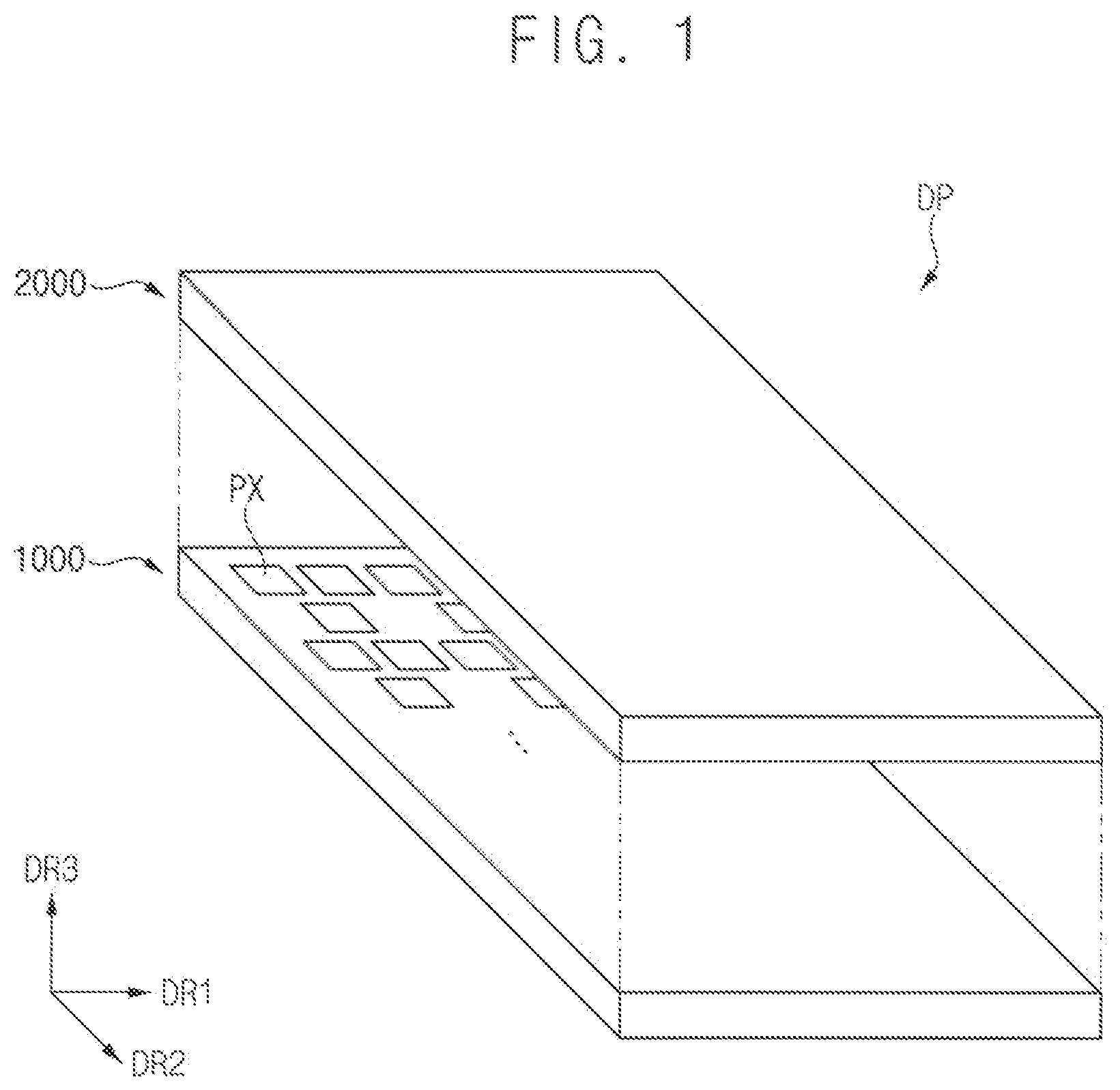
is a perspective view showing a display device according to one or more embodiments of the present disclosure.
Referring to , a display device DP may include an array substrate 1000 and a color conversion substrate 2000 .
The array substrate 1000 may include a light emitting element PX. The light emitting element PX may receive an electrical signal to emit light having a luminance corresponding to a level of the electrical signal.
The color conversion substrate 2000 may be disposed on the array substrate 1000 . The light emitted from the light emitting element PX may pass through the color conversion substrate 2000 . The color conversion substrate 2000 may convert a color of the light emitted from the light emitting element PX. For example, the light emitted from the light emitting element PX that is incident on the color conversion substrate 2000 may be converted into red light while passing through the color conversion substrate 2000 . As another example, the light emitted from the light emitting element PX may be converted into green light while passing through the color conversion substrate 2000 . The light passing through the color conversion substrate 2000 may be visually recognized by a user and may be used by the display device DP to form or display an image.
to 4 are views showing a color conversion substrate included in the display device of . may be a plan view showing a color conversion substrate 2000 of when viewed in a third direction DR 3 , may be a sectional view taken along the line of , and may be a sectional view taken along the line of .
Referring to to 4 , the color conversion substrate 2000 may include an upper substrate 100 , a color filter layer 110 , a low refraction layer 120 , a protective layer 130 , a color conversion layer 200 , and a bank 140 .
The upper substrate 100 may transmit the light emitted from the light emitting element PX. For example, the upper substrate 100 may be a transparent substrate. The upper substrate 100 may include an insulating material such as glass or plastic. Alternatively, the upper substrate 100 may include an organic polymer material such as polycarbonate (PC), polyethylene terephthalate (PET), polyethylene (PE), or polypropylene (PP).
The color filter layer 110 may be disposed on or under the upper substrate 100 . The color filter layer 110 may selectively transmit light having a specific wavelength. For example, the color filter layer 110 may include first to third color filter layers 111 , 112 , and 113 . The first color filter layer 111 may selectively transmit first light having a first wavelength, the second color filter layer 112 may selectively transmit second light having a second wavelength, and the third color filter layer 113 may selectively transmit third light having a third wavelength. In one or more embodiments, the first to third color filter layers 111 , 112 , and 113 may selectively transmit first to third light having different wavelengths from each other.
A light blocking layer may be disposed on or under the upper substrate 100 . The light emitted from the light emitting element PX may pass through only a partial region of the color conversion substrate 2000 . The partial region may be defined by the light blocking layer. For example, the light blocking layer may be disposed on a bottom surface of the upper substrate 100 to form a light blocking region BA through which the light emitted from the light emitting element PX does not pass. In this case, a region where the light blocking layer is not disposed on the bottom surface of the upper substrate 100 may be a transmissive region TA through which the light emitted from the light emitting element PX is transmitted.
According to one or more embodiments, the light blocking layer may be formed by stacking the first to third color filter layers 111 , 112 , and 113 such that the first to third color filter layers 111 , 112 , and 113 may overlap each other. For example, the first to third color filter layers 111 , 112 , and 113 may be stacked on the bottom surface of the upper substrate 100 such that the first to third color filter layers 111 , 112 , and 113 may overlap each other (e.g., overlap each other in a thickness direction of the upper substrate 100 ), so that the light blocking region BA through which the light emitted from the light emitting element PX does not pass may be formed.
According to one or more embodiments, the light blocking layer may include a light blocking material. The light blocking material may have a specific color.
The low refraction layer 120 may be disposed on or under the color filter layer 110 . The low refraction layer 120 may cover the color filter layer 110 . The low refraction layer 120 may have a relatively low refractive index. For example, a refractive index of the low refraction layer 120 may be lower than a refractive index of the color conversion layer 200 . The low refraction layer 120 may include an organic material. For example, the low refraction layer 120 may include an organic polymer material including silicon (Si).
The protective layer 130 may be disposed on or under the low refraction layer 120 . The protective layer 130 may cover the low refraction layer 120 . The protective layer 130 may block external impurities to prevent or substantially prevent the color filter layer 110 from being contaminated. The protective layer 130 may include an inorganic material. For example, the protective layer 130 may include silicon oxide, silicon nitride, aluminum nitride, and the like.
The bank 140 and the color conversion layer 200 may be disposed on or under the protective layer 130 . The bank 140 may include a first opening region OP 1 and a second opening region OP 2 . The first opening region OP 1 may overlap (e.g., overlap in the thickness direction of the upper substrate 100 ) the light emitting element PX, and the second opening region OP 2 may not overlap the light emitting element PX.
The second opening region OP 2 may overlap (e.g., overlap in the thickness direction of the upper substrate 100 ) the light blocking region BA. The color conversion layer 200 may be disposed in the first opening region OP 1 . The color conversion layer 200 may convert the light emitted from the light emitting element PX into light having a specific wavelength. For example, the color conversion layer 200 may include color conversion particles including quantum dots (QDs).
The color conversion layer 200 may be formed by an inkjet scheme. For example, the color conversion layer 200 may be formed by dropping an ink including the color conversion particles in the first opening region OP 1 . However, the ink may not be dropped in the first opening region OP 1 . In other words, the ink may be erroneously jetted. The erroneously jetted ink may be classified into a first erroneously jetted ink, a second erroneously jetted ink, and a third erroneously jetted ink according to a location where the erroneously jetted ink is dropped. The first erroneously jetted ink (e.g., IDA of ) may be an ink that is erroneously jetted in a central region CO or a peripheral region SO. The second erroneously jetted ink (e.g., IDB of ) may be an ink that is erroneously jetted on a first partition wall W 1 or a second partition wall W 2 . The third erroneously jetted ink (e.g., IDC of ) may be an ink that is erroneously jetted in a first region A where the first partition wall W 1 and the second partition wall W 2 make contact with each other.
According to one or more embodiments, the color conversion layer 200 may include first to third color conversion layers 201 , 202 , and 203 . The first color conversion layer 201 may include first color conversion particles, the second color conversion layer 202 may include scattering particles, and the third color conversion layer 203 may include second color conversion particles. Accordingly, the first color conversion layer 201 may convert the light emitted from the light emitting element PX into the first light, the second color conversion layer 202 may transmit the light emitted from the light emitting element PX, and the third color conversion layer 203 may convert the light emitted from the light emitting element PX into the third light.
The first color conversion particles may include a first scatterer and a first quantum dot having a first size. The first quantum dot may be excited by the light emitted from the light emitting element PX to emit the first light. Accordingly, the first color conversion layer 201 may convert the light emitted from the light emitting element PX into the first light.
The second color conversion layer 202 may include the scattering particles, and the light emitting element PX may emit the second light. Accordingly, the second color conversion layer 202 may transmit the second light emitted from the light emitting element PX. For example, the light emitting element PX may emit blue light, and the second color conversion layer 202 may transmit the blue light emitted from the light emitting element PX. As another example, the light emitting element PX may emit white light, and the second color conversion layer 202 may transmit the white light emitted from the light emitting element PX.
The second color conversion particles may include a second scatterer and a second quantum dot having a second size that is different from the first size. The second quantum dot may be excited by the light emitted from the light emitting element PX to emit the third light. Accordingly, the third color conversion layer 203 may convert the light emitted from the light emitting element PX into the third light.
According to one or more embodiments, the first opening region OP 1 may include first to third color conversion regions CA 1 , CA 2 , and CA 3 . The first color conversion layer 201 may be disposed in the first color conversion region CA 1 . The first color conversion region CA 1 may overlap (e.g., overlap in the thickness direction of the upper substrate 100 ) the first color filter layer 111 . In addition, at least a portion of the first color conversion region CA 1 may overlap (e.g., overlap in the thickness direction of the upper substrate 100 ) the transmissive region TA. Accordingly, the light emitted from the light emitting element PX may sequentially pass through the first color conversion layer 201 and the first color filter layer 111 so as to be visually recognized by the user as the first light having the first wavelength.
The second color conversion layer 202 may be disposed in the second color conversion region CA 2 . The second color conversion region CA 2 may overlap (e.g., overlap in the thickness direction of the upper substrate 100 ) the second color filter layer 112 . In addition, at least a portion of the second color conversion region CA 2 may overlap (e.g., overlap in the thickness direction of the upper substrate 100 ) the transmissive region TA. Accordingly, the light emitted from the light emitting element PX may sequentially pass through the second color conversion layer 202 and the second color filter layer 112 so as to be visually recognized by the user as the second light having the second wavelength.
The third color conversion layer 203 may be disposed in the third color conversion region CA 3 . The third color conversion region CA 3 may overlap (e.g., overlap in the thickness direction of the upper substrate 100 ) the third color filter layer 113 . In addition, at least a portion of the third color conversion region CA 3 may overlap (e.g., overlap in the thickness direction of the upper substrate 100 ) the transmissive region TA. Accordingly, the light emitted from the light emitting element PX may sequentially pass through the third color conversion layer 203 and the third color filter layer 113 so as to be visually recognized by the user as the third light having the third wavelength.
The second opening region OP 2 may be partitioned by the first partition wall W 1 and the second partition wall W 2 . The first partition wall W 1 may partition the second opening region OP 2 into a central region CO and a peripheral region SO. In one or more embodiments, the shape of the first partition wall W 1 corresponds to the shape of the central region CO. The peripheral region SO may be around (e.g., surround) the central region CO. For example, the central region CO may denote a region surrounded by the first partition wall W 1 in the second opening region OP 2 , and the peripheral region SO may denote a region outside the region surrounded by the first partition wall W 1 in the second opening region OP 2 . The central region CO and the peripheral region SO may receive the first erroneously jetted ink.
The first partition wall W 1 may have a polygonal shape including n vertices when viewed in a plan view (n is a natural number greater than or equal to 3). Accordingly, the central region CO may also have a polygonal shape when viewed in a plan view. Hereinafter, throughout the present disclosure, ‘n’ is defined as a term designating “a natural number greater than or equal to 3”.
The second partition wall W 2 may extend from each of the n vertices of the first partition wall W 1 to an edge of the second opening region OP 2 . In other words, the second partition wall W 2 may include n compartmental walls (e.g., P 1 to P 8 of ). Accordingly, the second partition wall W 2 may partition the peripheral region SO into n sub-regions (e.g., SO 1 to SO 8 of ). For example, sub-regions of the peripheral region SO may be spaced from each other by a compartmental wall of the second partition wall W 2 . Each of the n compartmental walls may be perpendicular to the edge of the second opening region OP 2 . In one or more embodiments, each of the sides of the central region CO may be opposite (e.g., face) respective sub-regions of the peripheral region SO. For example, a sub-region of the peripheral region SO and another sub-region of the peripheral region SO may be opposite (e.g., face) each other with the central region CO therebetween.
The second opening region OP 2 and the first opening region OP 1 may be partitioned by the bank 140 . The bank 140 (e.g., a portion of the bank 140 ) between the first opening region OP 1 and the second opening region OP 2 may be lost during a process of manufacturing the display device. For example, the bank 140 may be lost in a second region B between the second color conversion region CA 2 and the second opening region OP 2 . Because the color conversion substrate 2000 according to the embodiments includes the first partition wall W 1 and the second partition wall W 2 that partition the second opening region OP 2 , even when the bank 140 is lost, the color conversion layer 200 disposed in the first opening region OP 1 may be lost to only one of the n sub-regions.
According to one or more embodiments, an area of each of the n sub-regions may be smaller than an area of the central region CO. In other words, each of the n sub-regions may have a relatively small area. Accordingly, even when the bank 140 is lost, a relatively small amount of the color conversion layer 200 disposed in the first opening region OP 1 may be lost (e.g., lost to an n sub-region).
In one or more embodiments, the first partition wall W 1 may have a polygonal shape when viewed in a plan view, and the second partition wall W 2 may extend from each of vertices of the polygonal shape to the second opening region. Accordingly, the first region A where the first partition wall W 1 and the second partition wall W 2 make contact with each other may have a relatively small area. Because the first region A has a relatively small area, even when the third erroneously jetted ink is dropped in the first region A, the third erroneously jetted ink may have a relatively small size. In this case, a protrusion having a relatively small size or substantially no protrusion may be formed in the first region A where the first partition wall W 1 and the second partition wall W 2 contact each other.
According to one or more embodiments, a first thickness D 1 of the first partition wall W 1 and a second thickness D 2 of the second partition wall W 2 may be different from each other. Accordingly, even when the third erroneously jetted ink is dropped in the first region A, the third erroneously jetted ink may have a relatively small size. In this case, a protrusion having a relatively small size or substantially no protrusion may be formed in the first region A where the first partition wall W 1 and the second partition wall W 2 contact each other.
According to one or more embodiments, the first thickness D 1 may be about 5 μm or more and about 25 μm or less, and the second thickness D 2 may be about 5 μm or more and about 25 μm or less. In one or more embodiments, for example, the first thickness D 1 may be about 16 μm, and the second thickness D 2 may be about 14 μm. When the first thickness D 1 or the second thickness D 2 is less than about 5 μm, durability of the first partition wall W 1 or the second partition wall W 2 may be relatively reduced. In other words, the first partition wall W 1 or the second partition wall W 2 may be lost during the process of manufacturing the display device. When the first thickness D 1 or the second thickness D 2 is greater than about 25 μm, the second erroneously jetted ink dropped on the first partition wall W 1 or the second partition wall W 2 may have a relatively large size. In this case, a relatively large protrusion may be formed on the first partition wall W 1 or the second partition wall W 2 when the second erroneously jetted ink is dropped on the first partition wall W 1 or the second partition wall W 2 .
According to one or more embodiments, each of the n compartmental walls included in the second partition wall W 2 may be configured such that an angle between one of the n compartmental walls and the first partition wall W 1 making contact with the one compartmental wall may be greater than or equal to about 90 degrees. For example, an angle between a first compartmental wall P 1 of and a first side S 1 of the first partition wall W 1 of may be greater than or equal to about 90 degrees, and an angle between the first compartmental wall P 1 of and a second side S 2 of the first partition wall W 1 of may be greater than or equal to about 90 degrees. Accordingly, the first region A may have a relatively small area, and even when the third erroneously jetted ink is dropped in the first region A, the third erroneously jetted ink may have a relatively small size. In this case, a protrusion having a relatively small size or substantially no protrusion may be formed in the first region A where the first partition wall W 1 and the second partition wall W 2 contact each other.
The first to third color conversion regions CA 1 , CA 2 , and CA 3 may be partitioned by the bank 140 . For example, the bank 140 may be disposed between the first color conversion region CA 1 and the second color conversion region CA 2 . The bank 140 may block light emitted from the first color conversion region CA 1 from being irradiated to the second color conversion region CA 2 or the third color conversion region CA 3 , block light emitted from the second color conversion region CA 2 from being irradiated to the first color conversion region CA 1 or the third color conversion region CA 3 , and block light emitted from the third color conversion region CA 3 from being irradiated to the first color conversion region CA 1 or the second color conversion region CA 2 .
In one or more embodiments, the first light may be red light, the second light may be blue light, and the third light may be green light. Alternatively, the first light may be green light, the second light may be blue light, and the third light may be red light.
The color filter layer 110 and the color conversion layer 200 according to the embodiments of the present disclosure are not limited to the above-described embodiments. For example, the first color filter layer 111 may selectively transmit the third light, the second color filter layer 112 may selectively transmit the first light, and the third color filter layer 113 may selectively transmit the second light. In this case, the first color conversion layer 201 may convert the light emitted from the light emitting element PX into the third light, the second color conversion layer 202 may convert the light emitted from the light emitting element PX into the first light, and the third color conversion layer 203 may transmit the light emitted from the light emitting element PX.
is a plan view showing a second opening region according to one or more embodiments of the present disclosure. may be an enlarged plan view showing the second opening region OP 2 of .
Referring to , the first partition wall W 1 may have an octagonal shape including a first side S 1 , a second side S 2 making contact with the first side S 1 , a third side S 3 making contact with the second side S 2 , a fourth side S 4 making contact with the third side S 3 , a fifth side S 5 making contact with the fourth side S 4 , a sixth side S 6 making contact with the fifth side S 5 , a seventh side S 7 making contact with the sixth side S 6 , and an eighth side S 8 making contact with the first side S 1 and the seventh side S 7 when viewed in a plan view.
Accordingly, the second partition wall W 2 may include a first compartmental wall P 1 making contact with the first side S 1 and the second side S 2 , a second compartmental wall P 2 making contact with the second side S 2 and the third side S 3 , a third compartmental wall P 3 making contact with the third side S 3 and the fourth side S 4 , a fourth compartmental wall P 4 making contact with the fourth side S 4 and the fifth side S 5 , a fifth compartmental wall P 5 making contact with the fifth side S 5 and the sixth side S 6 , a sixth compartmental wall P 6 making contact with the sixth side S 6 and the seventh side S 7 , a seventh compartmental wall P 7 making contact with the seventh side S 7 and the eighth side S 8 , and an eighth compartmental wall P 8 making contact with the eighth side S 8 and the first side S 1 . The first to eighth compartmental walls P 1 , P 2 , P 3 , P 4 , P 5 , P 6 , P 7 , and P 8 may extend from eight vertices of the first partition wall W 1 having an octagonal shape to the edge of the second opening region OP 2 when viewed in a plan view, respectively. In one or more embodiments, each of the first to eighth compartmental walls P 1 , P 2 , P 3 , P 4 , P 5 , P 6 , P 7 , and P 8 may extend from a respective vertex of the first partition wall W 1 to an adjacent portion of the edge of the second opening region OP 2 as illustrated in .
The central region CO may have an octagonal shape surrounded by the first to eighth sides S 1 , S 2 , S 3 , S 4 , S 5 , S 6 , S 7 , and S 8 of the first partition wall W 1 when viewed in a plan view. The first to eighth compartmental walls P 1 , P 2 , P 3 , P 4 , P 5 , P 6 , P 7 , and P 8 may partition the peripheral region SO into first to eighth sub-regions SO 1 , SO 2 , SO 3 , SO 4 , SO 5 , SO 6 , SO 7 , and SO 8 . For example, the first sub-region SO 1 may be defined as a region partitioned by the first and eighth compartmental walls P 1 and P 8 , the first side S 1 of the first partition wall W 1 , and the edge of the second opening region OP 2 .
The first to eighth sides S 1 , S 2 , S 3 , S 4 , S 5 , S 6 , S 7 , and S 8 and the first to eighth compartmental walls P 1 , P 2 , P 3 , P 4 , P 5 , P 6 , P 7 , and P 8 may have various suitable arrangements. For example, the first to eighth sides S 1 , S 2 , S 3 , S 4 , S 5 , S 6 , S 7 , and S 8 and the first to eighth compartmental walls P 1 , P 2 , P 3 , P 4 , P 5 , P 6 , P 7 , and P 8 may have various suitable arrangements capable of allowing the first to eighth sub-regions SO 1 , SO 2 , SO 3 , SO 4 , SO 5 , SO 6 , SO 7 , and SO 8 to have a relatively small area, and allowing a region where the first partition wall W 1 and the second partition wall W 2 make contact with each other (e.g., a region C, which is a region where the first compartmental wall P 1 and the first partition wall W 1 make contact with each other) to have a relatively small area.
According to one or more embodiments, the first side S 1 and the fifth side S 5 may extend in a second direction DR 2 , and the third side S 3 and the seventh side S 7 may extend in a first direction DR 1 that is perpendicular to the second direction DR 2 . For example, each of the first compartmental wall P 1 and the eighth compartmental wall P 8 may be perpendicular to the first side S 1 , each of the second compartmental wall P 2 and the third compartmental wall P 3 may be perpendicular to the third side S 3 , each of the fourth compartmental wall P 4 and the fifth compartmental wall P 5 may be perpendicular to the fifth side S 5 , and each of the sixth compartmental wall P 6 and the seventh compartmental wall P 7 may be perpendicular to the seventh side S 7 .
According to one or more embodiments, each of the first to eighth compartmental walls P 1 , P 2 , P 3 , P 4 , P 5 , P 6 , P 7 , and P 8 may have a first length L 1 , each of the first, third, fifth, and seventh sides S 1 , S 3 , S 5 , and S 7 may have a second length L 2 , and each of the second, fourth, sixth, and eighth sides S 2 , S 4 , S 6 , and S 8 may have a third length L 3 . The first length L 1 and the second length L 2 may be different from each other, and the third length L 3 may be different from the first length L 1 and the second length L 2 . For example, the first length L 1 may be smaller than the second length L 2 . In addition, the first length L 1 may be smaller than the third length L 3 . In one or more embodiments, the second length L 2 may be different from the third length L 3 .
According to one or more embodiments, the first to eighth sides S 1 , S 2 , S 3 , S 4 , S 5 , S 6 , S 7 , and S 8 and the first to eighth compartmental walls P 1 , P 2 , P 3 , P 4 , P 5 , P 6 , P 7 , and P 8 may be symmetrically arranged with respect to the first direction DR 1 (e.g., symmetrically arranged about a reference line extending through a center of the central region CO in the first direction DR 1 ), and may be symmetrically arranged with respect to the second direction DR 2 (e.g., symmetrically arranged about a reference line extending through a center of the central region CO in the second direction DR 2 ).
is a plan view showing a second opening region according to another embodiment of the present disclosure.
Referring to , the first partition wall W 1 may have a hexagonal shape including a first side S 1 ′, a second side S 2 ′ making contact with the first side S 1 ′, a third side S 3 ′ making contact with the second side S 2 ′, a fourth side S 4 ′ making contact with the third side S 3 ′, a fifth side S 5 ′ making contact with the fourth side S 4 ′, and a sixth side S 6 ′ making contact with the first side S 1 ′ and the fifth side S 5 ′ when viewed in a plan view.
Accordingly, the second partition wall W 2 may include a first compartmental wall P 1 ′ making contact with the first side S 1 ′ and the second side S 2 ′, a second compartmental wall P 2 ′ making contact with the second side S 2 ′ and the third side S 3 ′, a third compartmental wall P 3 ′ making contact with the third side S 3 ′ and the fourth side S 4 ′, a fourth compartmental wall P 4 ′ making contact with the fourth side S 4 ′ and the fifth side S 5 ′, a fifth compartmental wall P 5 ′ making contact with the fifth side S 5 ′ and the sixth side S 6 ′, and a sixth compartmental wall P 6 ′ making contact with the first side S 1 ′ and the sixth side S 6 ′. The first to sixth compartmental walls P 1 ′, P 2 ′, P 3 ′, P 4 ′, P 5 ′, and P 6 ′ may extend from six vertices of the first partition wall W 1 having a hexagonal shape to the edge of the second opening region OP 2 when viewed in a plan view, respectively. In one or more embodiments, each of the first to sixth compartmental walls P 1 ′, P 2 ′, P 3 ′, P 4 ′, P 5 ′, and P 6 ′ may extend from a respective vertex of the first partition wall W 1 to an adjacent portion of the edge of the second opening region OP 2 as illustrated in .
A central region CO′ may have a hexagonal shape surrounded by the first to sixth sides S 1 ′, S 2 ′, S 3 ′, S 4 ′, S 5 ′, and S 6 ′ when viewed in a plan view. The first to sixth compartmental walls P 1 ′, P 2 ′, P 3 ′, P 4 ′, P 5 ′, and P 6 ′ may partition the peripheral region SO into first to sixth sub-regions SO 1 ′, SO 2 ′, SO 3 ′, SO 4 ′, SO 5 ′, and SO 6 ′. For example, the first sub-region SO 1 ′ may be defined as a region partitioned by the first and sixth compartmental walls P 1 ′ and P 6 ′, the first side S 1 ′ of the first partition wall W 1 , and the edge of the second opening region OP 2 .
The first to sixth sides S 1 ′, S 2 ′, S 3 ′, S 4 ′, S 5 ′, and S 6 ′ and the first to sixth compartmental walls P 1 ′, P 2 ′, P 3 ′, P 4 ′, P 5 ′, and P 6 ′ may have various suitable arrangements. For example, the first to sixth sides S 1 ′, S 2 ′, S 3 ′, S 4 ′, S 5 ′, and S 6 ′ and the first to sixth compartmental walls P 1 ′, P 2 ′, P 3 ′, P 4 ′, P 5 ′, and P 6 ′ may have various suitable arrangements capable of allowing the first to sixth sub-regions SO 1 ′, SO 2 ′, SO 3 ′, SO 4 ′, SO 5 ′, and SO 6 ′ to have a relatively small area, and allowing a region where the first partition wall W 1 and the second partition wall W 2 make contact with each other (e.g., a region D, which is a region where the first compartmental wall P 1 ′ and the first partition wall W 1 make contact with each other) to have a relatively small area.
According to one or more embodiments, the first side S 1 ′ and the fourth side S 4 ′ may be parallel to each other, the second side S 2 ′ and the fifth side S 5 ′ may be parallel to each other, and the third side S 3 ′ and the sixth side S 6 ′ may be parallel to each other. In this case, each of the first compartmental wall P 1 ′ and the sixth compartmental wall P 6 ′ may be perpendicular to the first side S 1 ′, and each of the third compartmental wall P 3 ′ and the fourth compartmental wall P 4 ′ may be perpendicular to the fourth side S 4 ′.
According to one or more embodiments, the first to sixth sides S 1 ′, S 2 ′, S 3 ′, S 4 ′, S 5 ′, and S 6 ′ and the first to sixth compartmental walls P 1 ′, P 2 ′, P 3 ′, P 4 ′, P 5 ′, and P 6 ′ may be symmetrically arranged with respect to the first direction DR 1 (e.g., symmetrically arranged about a reference line extending through a center of the central region CO′ in the first direction DR 1 ), and may be symmetrically arranged with respect to the second direction DR 2 (e.g., symmetrically arranged about a reference line extending through a center of the central region CO′ in the second direction DR 2 ).
is a plan view showing a second opening region according to still another embodiment of the present disclosure.
Referring to , the first partition wall W 1 may have a rectangular shape including a first side S 1 ″, a second side S 2 ″ making contact with the first side S 1 ″, a third side S 3 ″ making contact with the second side S 2 ″, and a fourth side S 4 ″ making contact with the first side S 1 ″ and the third side S 3 ″ when viewed in a plan view.
Accordingly, the second partition wall W 2 may include a first compartmental wall P 1 ″ making contact with the first side S 1 ″ and the second side S 2 ″, a second compartmental wall P 2 ″ making contact with the second side S 2 ″ and the third side S 3 ″, a third compartmental wall P 3 ″ making contact with the third side S 3 ″ and the fourth side S 4 ″, and a fourth compartmental wall P 4 ″ making contact with the first side S 1 ″ and the fourth side S 4 ″. The first to fourth compartmental walls P 1 ″, P 2 ″, P 3 ″, and P 4 ″ may extend from four vertices of the first partition wall W 1 having a rectangular shape to the edge of the second opening region OP 2 when viewed in a plan view, respectively. In one or more embodiments, each of the first to fourth compartmental walls P 1 ″, P 2 ″, P 3 ″, and P 4 ″ may extend from a respective vertex of the first partition wall W 1 to an adjacent portion of the edge of the second opening region OP 2 as illustrated in .
A central region CO″ may have a rectangular shape surrounded by the first to fourth sides S 1 ″, S 2 ″, S 3 ″, and S 4 ″ when viewed in a plan view. The first to fourth compartmental walls P 1 ″, P 2 ″, P 3 ″, and P 4 ″ may partition the peripheral region SO into first to fourth sub-regions 501 ″, SO 2 ″, SO 3 ″, and SO 4 ″. For example, the first sub-region SO 1 ″ may be defined as a region partitioned by the first and fourth compartmental walls P 1 ″ and P 4 ″, the first side S 1 ″ of the first partition wall W 1 , and the edge of the second opening region OP 2 .
The first to fourth sides S 1 ″, S 2 ″, S 3 ″, and S 4 ″ and the first to fourth compartmental walls P 1 ″, P 2 ″, P 3 ″, and P 4 ″ may have various suitable arrangements. For example, the first to fourth sides S 1 ″, S 2 ″, S 3 ″, and S 4 ″ and the first to fourth compartmental walls P 1 ″, P 2 ″, P 3 ″, and P 4 ″ may have various suitable arrangements capable of allowing the first to fourth sub-regions SO 1 ″, SO 2 ″, SO 3 ″, and SO 4 ″ to have a relatively small area, and allowing a region where the first partition wall W 1 and the second partition wall W 2 make contact with each other (e.g., a region E, which is a region where the first compartmental wall P 1 ″ and the first partition wall W 1 make contact with each other) to have a relatively small area.
is a perspective view showing a display device according to one or more embodiments of the present disclosure. is a plan view showing an array substrate included in the display device of . is a plan view showing a color conversion substrate included in the display device of . is a sectional view taken along the line III-III′ of . is a sectional view taken along the line IV-IV′ of . may be a plan view showing an array substrate 1000 of when viewed in a direction opposite to the third direction DR 3 , and may be a plan view showing a color conversion substrate 2000 of when viewed in the third direction DR 3 .
Referring to , may be a perspective view showing a state in which the array substrate 1000 and the color conversion substrate 2000 of are coupled to each other. In other words, the array substrate 1000 of may be substantially the same as the array substrate 1000 described with reference to to 7 , and the color conversion substrate 2000 of may be substantially the same as the color conversion substrate 2000 described with reference to to 7 except for a third opening region OP 3 and the fourth opening region OP 4 . Therefore, redundant descriptions of configurations of to 7 may not be repeated below.
Referring to , 9 , 11 , and 12 , the array substrate 1000 may include a lower substrate 300 , a pixel defining layer 310 , first to third electrodes 321 E, 322 E, and 323 E, first to third light emitting layers 321 L, 322 L, and 323 L, a common electrode 330 , and an encapsulation layer 340 . The array substrate 1000 may include a light emitting element PX. The light emitting element PX may include first to third light emitting elements PX 1 , PX 2 , and PX 3 . The first light emitting element PX 1 may include the first electrode 321 E and the first light emitting layer 321 L, the second light emitting element PX 2 may include the second electrode 322 E and the second light emitting layer 322 L, and the third light emitting element PX 3 may include the third electrode 323 E and the third light emitting layer 323 L. The light emitting element PX may be disposed in a display region DA.
The lower substrate 300 may include at least one transistor and at least one driver. The transistor may be electrically connected to the driver. The transistor may generate an electrical signal. The transistor may be disposed in the display region DA. The driver may be disposed in a peripheral region SA surrounding the display region DA. Although an embodiment in which the peripheral region SA surrounds the display region DA has been shown in , the present disclosure is not limited thereto. For example, the peripheral region SA may be omitted, and the driver may be disposed in the display region DA.
The first to third electrodes 321 E, 322 E, and 323 E may be disposed on the lower substrate 300 . Each of the first to third electrodes 321 E, 322 E, and 323 E may be electrically connected to the transistor. The first to third electrodes 321 E, 322 E, and 323 E may be referred to as anode electrodes.
The pixel defining layer 310 may be disposed on the lower substrate 300 . The pixel defining layer 310 may include first to third openings that partially expose top surfaces of the first to third electrodes 321 E, 322 E, and 323 E, respectively.
The first to third light emitting layers 321 L, 322 L, and 323 L may be disposed on the first to third electrodes 321 E, 322 E, and 323 E exposed by the first to third openings, respectively. For example, the first light emitting layer 321 L may be disposed on the first electrode 321 E exposed by the first opening. The first to third light emitting layers 321 L, 322 L, and 323 L may emit light having a luminance corresponding to a level of the electric signal. For example, the first to third light emitting layers 321 L, 322 L, and 323 L may emit blue light. As another example, the first to third light emitting layers 321 L, 322 L, and 323 L may emit white light.
The common electrode 330 may be disposed on the pixel defining layer 310 and the first to third light emitting layers 321 L, 322 L, and 323 L. The common electrode 330 may be referred to as a cathode electrode.
The encapsulation layer 340 may cover the common electrode 330 . The encapsulation layer 340 may include a first inorganic layer, a first organic layer, and a second inorganic layer. The first inorganic layer may be disposed on and cover the common electrode 330 , the first organic layer may be disposed on and cover the first inorganic layer, and the second inorganic layer may be disposed on and cover the first organic layer. The encapsulation layer 340 may block external impurities.
According to one or more embodiments, the array substrate 1000 may include a first light emitting element row X 1 and a second light emitting element row X 2 . The first light emitting element row X 1 may include a first light emitting element PX 1 and a second light emitting element PX 2 , which are alternately arranged in or along the first direction DR 1 , and the second light emitting element row X 2 may include third light emitting elements PX 3 arranged (e.g., repeatedly arranged) in or along the first direction DR 1 . The second light emitting element row X 2 may be spaced from the first light emitting element row X 1 in the second direction DR 2 . The first light emitting element row X 1 and the second light emitting element row X 2 may be alternately arranged in or along the second direction DR 2 . Each of the first light emitting element PX 1 , the second light emitting element PX 2 , and the third light emitting element PX 3 may have a square shape having the same area when viewed in a plan view.
According to one or more embodiments, each of the first light emitting element PX 1 , the second light emitting element PX 2 , and the third light emitting element PX 3 may have a circular shape when viewed in a plan view. Alternatively, each of the first light emitting element PX 1 , the second light emitting element PX 2 , and the third light emitting element PX 3 may have a polygonal shape when viewed in a plan view. In one or more embodiments, the first light emitting element PX 1 , the second light emitting element PX 2 , and the third light emitting element PX 3 may have mutually different areas. For example, an area of the third light emitting element PX 3 may be larger than an area of the second light emitting element PX 2 and/or an area of the first light emitting element PX 1 when viewed in a plan view.
Referring to to 12 , the array substrate 1000 and the color conversion substrate 2000 may overlap each other. In detail, the light emitting element PX of the array substrate 1000 may overlap (e.g., overlap in the thickness direction of the upper substrate 100 ) the first opening region OP 1 of the color conversion substrate 2000 . For example, the first color conversion region CA 1 may overlap (e.g., overlap in the thickness direction of the upper substrate 100 ) the first light emitting element PX 1 , the second color conversion region CA 2 may overlap (e.g., overlap in the thickness direction of the upper substrate 100 ) the second light emitting element PX 2 , and the third color conversion region CA 3 may overlap (e.g., overlap in the thickness direction of the upper substrate 100 ) the third light emitting element PX 3 .
The color conversion substrate 2000 may include a first color conversion row X 1 ′ and a second color conversion row X 2 ′. The first color conversion row X 1 ′ may include the first color conversion region CA 1 and the second color conversion region CA 2 , which are alternately arranged in or along the first direction DR 1 , and the second color conversion row X 2 ′ may include the third color conversion region CA 3 and the second opening region OP 2 , which are alternately arranged in or along the first direction DR 1 . The first color conversion row X 1 ′ and the second color conversion row X 2 ′ may be alternately arranged in or along the second direction DR 2 .
According to one or more embodiments, each of the first color conversion region CA 1 , the second color conversion region CA 2 , and the third color conversion region CA 3 may have a rectangular shape having a first area when viewed in a plan view. The second opening region OP 2 may have a rectangular shape having a second area that is larger than the first region when viewed in a plan view.
According to one or more embodiments, each of the first color conversion region CA 1 , the second color conversion region CA 2 , and the third color conversion region CA 3 may have a circular shape when viewed in a plan view. Alternatively, each of the first color conversion region CA 1 , the second color conversion region CA 2 , and the third color conversion region CA 3 may have a polygonal shape when viewed in a plan view. In this case, the second opening region OP 2 may have various suitable shapes capable of minimizing or reducing a thickness of the bank 140 that partitions the first opening region OP 1 and the second opening region OP 2 when viewed in a plan view.
According to one or more embodiments, the first color conversion region CA 1 , the second color conversion region CA 2 , and the third color conversion region CA 3 may have mutually different areas when viewed in a plan view. For example, an area of the third color conversion region CA 3 may be larger than an area of the second color conversion region CA 2 when viewed in a plan view, and the area of the second color conversion region CA 2 may be larger than an area of the first color conversion region CA 1 when viewed in a plan view.
According to one or more embodiments, the area of the third color conversion region CA 3 may be larger than the area of the first color conversion region CA 1 , and larger than the area of the second color conversion region CA 2 when viewed in a plan view. In this case, the area of the first color conversion region CA 1 and the area of the second color conversion region CA 2 may be substantially the same when viewed in a plan view.
According to one or more embodiments, the color conversion substrate 2000 may further include a third opening region OP 3 and a fourth opening region OP 4 . The third opening region OP 3 may be located between the first color conversion region CA 1 and the second color conversion region CA 2 . A width W 1 ′ of the third opening region OP 3 in the first direction DR 1 may be smaller than a width W 2 ′ of the first color conversion region CA 1 in the first direction. In addition, the width W 1 ′ of the third opening region OP 3 in the first direction DR 1 may be smaller than a width W 3 ′ of the second color conversion region CA 2 in the first direction. The fourth opening region OP 4 may be located between the third color conversion region CA 3 and the first color conversion row X 1 ′. A width W 4 ′ of the fourth opening region OP 4 in the second direction DR 2 may be smaller than a width W 5 ′ of the third color conversion region CA 3 in the second direction DR 2 .
The third opening region OP 3 may prevent or substantially prevent the first color conversion layer 201 in the first color conversion region CA 1 from being lost to the second color conversion region CA 2 that is adjacent to the first color conversion layer 201 . In addition, the third opening region OP 3 may prevent or substantially prevent the second color conversion layer 202 in the second color conversion region CA 2 from being lost to the first color conversion region CA 1 that is adjacent to the second color conversion layer 202 .
The fourth opening region OP 4 may prevent or substantially prevent the third color conversion layer 203 in the third color conversion region CA 3 from being lost to the first and second color conversion regions CA 1 and CA 2 that are adjacent to the third color conversion layer 203 . In addition, the fourth opening region OP 4 may prevent or substantially prevent the first and second color conversion layers 201 and 202 in the first and second color conversion regions CA 1 and CA 2 from being lost to the third color conversion region CA 3 .
According to one or more embodiments, a filling layer 400 may be disposed between the color conversion substrate 2000 and the array substrate 1000 . The filling layer 400 may include a transmissive transparent material. The filling layer 400 may maintain a filling gap between the color conversion substrate 2000 and the array substrate 1000 . In addition, the filling layer 400 may be disposed in the first to fourth opening regions OP 1 , OP 2 , OP 3 , and OP 4 . In one or more embodiments, the filling layer 400 may be omitted.
to 21 are views showing a method of manufacturing a color conversion substrate according to one or more embodiments of the present disclosure. is a sectional view taken along the line V-V′ of , is a sectional view taken along the line VI-VI′ of , is a sectional view taken along the line VII-VII′ of , is a sectional view taken along the line VIII-VIII′ of , and is a sectional view taken along the line IX-IX′ of .
Referring to , a color filter layer 110 may be formed on an upper substrate 100 . The color filter layer 110 may include first to third color filter layers 111 , 112 , and 113 . During a process of forming the color filter layer 110 , the first to third color filter layers 111 , 112 , and 113 may be stacked on a partial region of the upper substrate 100 such that the first to third color filter layers 111 , 112 , and 113 may overlap each other. The partial region may be a light blocking region through which light does not pass. A low refraction layer 120 may be formed on the color filter layer 110 . A protective layer 130 may be formed on the low refraction layer 120 . A preliminary bank 141 may be formed on the protective layer 130 . The upper substrate 100 , the color filter layer 110 , the low refraction layer 120 , and the protective layer 130 may be substantially the same as the upper substrate 100 , the color filter layer 110 , the low refraction layer 120 , and the protective layer 130 , respectively, described with reference to to 4 .
Referring to , the preliminary bank 141 may be etched to form a bank 140 , a first partition wall W 1 , and a second partition wall W 2 .
In this case, a width (e.g., D 1 of ) of the first partition wall W 1 may be relatively small, and a width (e.g., D 2 of ) of the second partition wall W 2 may be relatively small.
In addition, a region (e.g., the region C of ) where the first partition wall W 1 and the second partition wall W 2 make contact with each other may have a relatively small area. For example, each of the width (e.g., D 1 of ) of the first partition wall W 1 and the width (e.g., D 2 of ) of the second partition wall W 2 may be relatively small. As another example, an angle between the first partition wall W 1 and the second partition wall W 2 may be adjusted, so that the region where the first partition wall W 1 and the second partition wall W 2 make contact with each other may have a relatively small area.
The bank 140 may include a first opening region OP 1 and a second opening region OP 2 . The second opening region OP 2 may include a central region CO and a peripheral region SO. The bank 140 , the first partition wall W 1 , and the second partition wall W 2 may be substantially the same as the bank 140 , the first partition wall W 1 , and the second partition wall W 2 , respectively, described with reference to to 4 .
Referring to to 19 , an inkjet head H may drop an ink ID including color conversion particles in the first opening region OP 1 . The inkjet head H may repeatedly drop the ink ID in the first opening region OP 1 to form a first color conversion layer 201 .
In addition, the inkjet head H may drop the ink ID in the second opening region OP 2 . The ink ID that is dropped in the second opening region OP 2 may be referred to as an erroneously jetted ink. The erroneously jetted ink may be classified into a first erroneously jetted ink IDA, a second erroneously jetted ink IDB, and a third erroneously jetted ink IDC according to a location where the erroneously jetted ink is dropped.
The first erroneously jetted ink IDA may be an ink that is erroneously jetted in the central region CO or the peripheral region SO. The first erroneously jetted ink IDA may be received in the central region CO or the peripheral region SO, and may not form a protrusion on the bank 140 .
The second erroneously jetted ink IDB may be an ink that is erroneously jetted on the first partition wall W 1 or the second partition wall W 2 . The second erroneously jetted ink IDB may form a protrusion on the first partition wall W 1 or the second partition wall W 2 . According to the present disclosure, the width (e.g., D 1 of ) of the first partition wall W 1 may be relatively small, and the width (e.g., D 2 of ) of the second partition wall W 2 may be relatively small. Accordingly, when an ink is erroneously jetted on the first partition wall W 1 or the second partition wall W 2 , a protrusion having a relatively small size may be formed on the first partition wall W 1 or the second partition wall W 2 , or no protrusion may be formed.
The third erroneously jetted ink IDC may be an ink that is erroneously jetted in a region where the first partition wall W 1 and the second partition wall W 2 make contact with each other. The third erroneously jetted ink IDC may form a protrusion in the region where the first partition wall W 1 and the second partition wall W 2 make contact with each other. According to the present disclosure, the region (e.g., the region C of ) where the first partition wall W 1 and the second partition wall W 2 make contact with each other may have a relatively small area. Accordingly, when an ink is erroneously jetted in the region where the first partition wall W 1 and the second partition wall W 2 make contact with each other, a protrusion having a relatively small size may be formed, or no protrusion may be formed.
Referring to , the first color conversion layer 201 may be formed in the first opening region OP 1 . The first color conversion layer 201 may be substantially the same as the first color conversion layer 201 described with reference to .
The color conversion substrate according to one or more embodiments of the present disclosure may be applied to various display devices, electronic devices, portable devices, communication devices, and/or the like. For example, the color conversion substrate according to the one or more embodiments of the present disclosure may be applied to a computer, a mobile phone, a smartphone, a smart pad, a TV, and/or the like.
Although embodiments of the present disclosure have been described above, it will be understood by those skilled in the art that various changes and modifications can be made to the present disclosure without departing from the spirit and scope of the present disclosure as set forth in the appended claims, and equivalents thereof.
Figures (20)
Citations
This patent cites (10)
- US12075678
- US2004/0252088
- US2012/0097991
- US2015/0084144
- US2020/0110303
- US111736388
- US2006-0072176
- US2013109907
- US2013254093
- US10-2021-0000184