Abstract
A memory system includes a nonvolatile memory and a memory controller. The memory controller is configured to: execute a first tracking process to determine a value of a first voltage in a patrol process that is carried out independently of a request from a host, execute a first data read process to read first data from the nonvolatile memory in response to receiving a read request from the host, cause the nonvolatile memory to execute a second tracking process using the first voltage when error correction of the first data fails, receive a value of a second voltage from the nonvolatile memory as a result of the second tracking process, and execute a second data read process using the second voltage to read second data from the nonvolatile memory.
Claims (20)
1. A memory system comprising: a nonvolatile memory including a plurality of memory cells; and a memory controller configured to execute a data read process of reading data from the plurality of memory cells, wherein the memory controller is further configured to: execute a first tracking process to determine a value of a first voltage in a patrol process that is carried out independently of a request from a host; execute a first data read process to read first data from the nonvolatile memory in response to receiving a read request from the host; cause the nonvolatile memory to execute a second tracking process using the first voltage when error correction of the first data fails; receive a value of a second voltage from the nonvolatile memory as a result of the second tracking process; and execute a second data read process using the second voltage to read second data from the nonvolatile memory.
11. A method of controlling a nonvolatile memory, the nonvolatile memory including a plurality of memory cells, said method comprising: executing a first tracking process to determine a value of a first voltage in a patrol process that is carried out independently of a request from a host; executing a first data read process that is responsive to a read request from the host to read first data from the nonvolatile memory; determining that error correction of the first data fails; in response to determining that the error correction of the first data fails, causing the nonvolatile memory to execute a second tracking process using the first voltage; receiving a value of a second voltage from the nonvolatile memory as a result of the second tracking process; and executing a second data read process using the second voltage to read second data from the nonvolatile memory.
Show 18 dependent claims
2. The memory system according to claim 1 , wherein in the patrol process, the memory controller: executes the first tracking process using a third voltage to determine a value of a fourth voltage; executes a third data read process using the fourth voltage to read third data from the nonvolatile memory; and determines the value of the fourth voltage as the value of the first voltage when error correction of the third data is successful.
3. The memory system according to claim 2 , wherein during the first tracking process, the memory controller: determines a search range based on a value of the third voltage; executes a plurality of data read processes while shifting a read voltage in the search range by a predetermined shift amount; and determines, as the fourth voltage, a read voltage at which the number of memory cells in an ON state among the plurality of memory cells satisfies a first condition.
4. The memory system according to claim 2 , wherein during the first tracking process, the memory controller: executes a plurality of data read processes using a plurality of read voltages, respectively; counts the number of memory cells in an ON state among the plurality of memory cells in each of the plurality of data read processes; and determines the value of the fourth voltage from (A) a value of a fifth voltage that is a maximum read voltage among read voltages at which the number of the memory cells in the ON state is smaller than an expected value and (B) a value of a sixth voltage that is a minimum read voltage among read voltages at which the number of the memory cells in the ON state is larger than the expected value.
5. The memory system according to claim 4 , wherein the memory controller is configured to: calculate a difference, as a first difference, between the expected value and a first number that is the number of the memory cells in the ON state in a data read process using the fifth voltage; calculate a difference, as a second difference, between the first number and a second number that is the number of the memory cells in the ON state in a data read process using the sixth voltage; calculate a difference, as a third difference, between the value of the fifth voltage and the value of the sixth voltage; multiply a ratio between the first difference and the second difference by the third difference; and add a result of the multiplication to the value of the fifth voltage to determine the value of the fourth voltage.
6. The memory system according to claim 2 , wherein during the first tracking process, the memory controller: executes a plurality of data read processes using a plurality of read voltages, respectively; when the number of memory cells in an ON state among the plurality of memory cells is smaller than an expected value in a fourth data read process among the plurality of data read processes, increases a read voltage and executes a fifth data read process among the plurality of data read processes; and when the number of the memory cells in the ON state is larger than the expected value in a sixth data read process among the plurality of data read processes, decreases a read voltage and executes a seventh data read process among the plurality of data read processes.
7. The memory system according to claim 6 , wherein the fourth data read process is executed using a seventh voltage, the sixth data read process is executed using an eighth voltage, and the memory controller determines the value of the fourth voltage based on a value of a first voltage difference that is a difference between a value of the seventh voltage and a value of the eighth voltage.
8. The memory system according to claim 7 , wherein when the value of the first voltage difference is larger than a threshold, the memory controller subtracts a value of a second voltage difference smaller than the value of the first voltage difference from the value of the seventh voltage or adds the value of the second voltage difference to the value of the eighth voltage to determine the value of the fourth voltage.
9. The memory system according to claim 1 , wherein in the patrol process, the memory controller: executes an eighth data read process using a ninth voltage to read fourth data from the nonvolatile memory; executes an error correction process on the fourth data to acquire fifth data; and determines the value of the first voltage from a value of the ninth voltage based on a difference between the number of bits having a first value in the fourth data and the number of bits having a second value in the fifth data.
10. The memory system according to claim 1 , wherein during the second tracking process, the nonvolatile memory: determines a read voltage based on the first voltage; executes a plurality of data read processes while shifting the read voltage; and estimates the value of the second voltage based on the plurality of data read processes.
12. The method according to claim 11 , wherein the patrol process includes the steps of: executing the first tracking process using a third voltage to determine a value of a fourth voltage; executing a third data read process using the fourth voltage to read third data from the nonvolatile memory; determining that error correction of the third data is successful; and in response to determining that the error correction of the third data is successful, determining the value of the fourth voltage as the value of the first voltage.
13. The method according to claim 12 , wherein the first tracking process includes the steps of: determining a search range based on a value of the third voltage; executing a plurality of data read processes while shifting a read voltage in the search range by a predetermined shift amount; and determining, as the fourth voltage, a read voltage at which the number of memory cells in an ON state among the plurality of memory cells satisfies a first condition.
14. The method according to claim 12 , wherein the first tracking process includes the steps of: executing a plurality of data read processes using a plurality of read voltages, respectively; counting the number of memory cells in an ON state among the plurality of memory cells in each of the plurality of data read processes; and determining the value of the fourth voltage from (A) a value of a fifth voltage that is a maximum read voltage among read voltages at which the number of the memory cells in the ON state is smaller than an expected value and (B) a value of a sixth voltage that is a minimum read voltage among read voltages at which the number of the memory cells in the ON state is larger than the expected value.
15. The method according to claim 14 , further comprising: calculating a difference, as a first difference, between the expected value and a first number that is the number of the memory cells in the ON state in a data read process using the fifth voltage; calculating a difference, as a second difference, between the first number and a second number that is the number of the memory cells in the ON state in a data read process using the sixth voltage; calculating a difference, as a third difference, between the value of the fifth voltage and the value of the sixth voltage; multiplying a ratio between the first difference and the second difference by the third difference; and adding a result of the multiplication to the value of the fifth voltage to determine the value of the fourth voltage.
16. The method according to claim 12 , wherein the first tracking process includes the steps of: executing a plurality of data read processes using a plurality of read voltages, respectively; determining that the number of memory cells in an ON state among the plurality of memory cells is smaller than an expected value in a fourth data read process among the plurality of data read processes; in response to determining that the number of the memory cells in the ON state among the plurality of memory cells is smaller than the expected value in the fourth data read process, increasing a read voltage and executing a fifth data read process among the plurality of data read processes; determining that the number of the memory cells in the ON state is larger than the expected value in a sixth data read process among the plurality of data read processes; in response to determining that the number of the memory cells in the ON state is larger than the expected value in the sixth data read process, decreasing a read voltage and executing a seventh data read process among the plurality of data read processes.
17. The method according to claim 16 , wherein the fourth data read process is executed using a seventh voltage, the sixth data read process is executed using an eighth voltage, and the value of the fourth voltage is determined based on a value of a first voltage difference that is a difference between a value of the seventh voltage and a value of the eighth voltage.
18. The method according to claim 17 , further comprising: determining that the value of the first voltage difference is larger than a threshold; and in response to determining that the value of the first voltage difference is larger than the threshold, subtracting a value of a second voltage difference smaller than the value of the first voltage difference from the value of the seventh voltage or adding the value of the second voltage difference to the value of the eighth voltage to determine the value of the fourth voltage.
19. The method according to claim 11 , wherein the patrol process includes the steps of: executing an eighth data read process using a ninth voltage to read fourth data from the nonvolatile memory; executing an error correction process on the fourth data to acquire fifth data; and determining the value of the first voltage from a value of the ninth voltage based on a difference between the number of bits having a first value in the fourth data and the number of bits having a second value in the fifth data.
20. The method according to claim 11 , wherein the second tracking process executed by the nonvolatile memory includes the steps of: determining a read voltage based on the first voltage; executing a plurality of data read processes while shifting the read voltage; and estimating the value of the second voltage based on the plurality of data read processes.
Full Description
Show full text →
CROSS-REFERENCE TO RELATED APPLICATION(S)
This application is based upon and claims the benefit of priority from Japanese Patent Application No. 2023-021015, filed Feb. 14, 2023, the entire contents of which are incorporated herein by reference.
FIELD
Embodiments described herein relate generally to a memory system.
BACKGROUND
A memory system including a nonvolatile memory such as a NAND flash memory and a memory controller that controls the nonvolatile memory is known.
DESCRIPTION OF THE DRAWINGS
is a block diagram illustrating a configuration of an information processing system according to a first embodiment.
is a block diagram illustrating an example of a signal used in a memory bus according to the first embodiment.
is a circuit diagram illustrating an example of a configuration of a nonvolatile memory according to the first embodiment.
is a schematic diagram illustrating an example of threshold voltage distributions of a plurality of memory cell transistors, and an example of a cumulative distribution function, according to the first embodiment.
is a diagram illustrating a configuration of shift amount information used in a memory system according to the first embodiment.
A and 6 B are schematic diagrams illustrating another example of threshold voltage distributions of the plurality of memory cell transistors, and another example of cumulative distribution function, according to the first embodiment.
A and 7 B are schematic diagrams illustrating still another example of threshold voltage distributions of the plurality of memory cell transistors, and still another example of cumulative distribution function, according to the first embodiment.
is a flowchart illustrating an example of a patrol process in the memory system according to the first embodiment.
is a flowchart illustrating an example of a tracking process in the memory system according to the first embodiment.
is a flowchart illustrating an example of the tracking process in the memory system according to the first embodiment.
is a diagram illustrating an initial value of a shift amount used in the tracking process in the memory system according to the first embodiment.
is a diagram illustrating the shift amount used in the tracking process in the memory system according to the first embodiment.
is a diagram illustrating a changed initial value of the shift amount used in the tracking process in the memory system according to the first embodiment.
is a diagram illustrating another changed initial value of the shift amount used in the tracking process in the memory system according to the first embodiment.
is a diagram illustrating a suitable shift amount calculated in the tracking process in the memory system according to the first embodiment.
is a flowchart illustrating an example of a host read process in the memory system according to the first embodiment.
is a block diagram illustrating a configuration of an information processing system according to a second embodiment.
is a diagram illustrating an example of a configuration of a lookup table used in the memory system according to the second embodiment.
is a flowchart illustrating an example of a tracking process in the memory system according to the second embodiment.
is a flowchart illustrating an example of the tracking process in the memory system according to the second embodiment.
is a diagram illustrating a suitable shift amount calculated in the tracking process in the memory system according to the second embodiment.
is a diagram illustrating a specific example of the tracking process in the memory system according to the second embodiment.
A to 23 C are diagrams illustrating an example of a first estimation method that is applied to a shift amount estimation process in a memory system according to a modification example.
A to 24 C are diagrams illustrating an example of a second estimation method that is applied to a shift amount estimation process in the memory system according to the modification example.
DETAILED DESCRIPTION
Embodiments provide a memory system where an operating speed is improved.
In general, according to one embodiment, a memory system includes a nonvolatile memory including a plurality of memory cells, and a memory controller configured to execute a data read process of reading data from the plurality of memory cells. Further, the memory controller is configured to execute a first tracking process to determine a value of a first voltage in a patrol process that is carried out independently of a request from a host. Further, the memory controller is configured to execute a first data read process to read first data from the nonvolatile memory in response to receiving a read request from the host and to cause the nonvolatile memory to execute a second tracking process using the first voltage when error correction of the first data fails. Further, the memory controller is configured to receive a value of a second voltage from the nonvolatile memory as a result of the second tracking process and to execute a second data read process using the second voltage to read second data from the nonvolatile memory.
Hereinafter, embodiments will be described with reference to the drawings. In the following description, components having substantially the same function and configuration will be denoted by the same reference numerals. In addition, the following embodiments show an example of technical ideas. The embodiments do not limit materials, shapes, structures, arrangement, and the like of components that may be used. Various changes can be made for other embodiments.
<1> First Embodiment
<1-1> Configuration
<1-1-1> Information Processing System
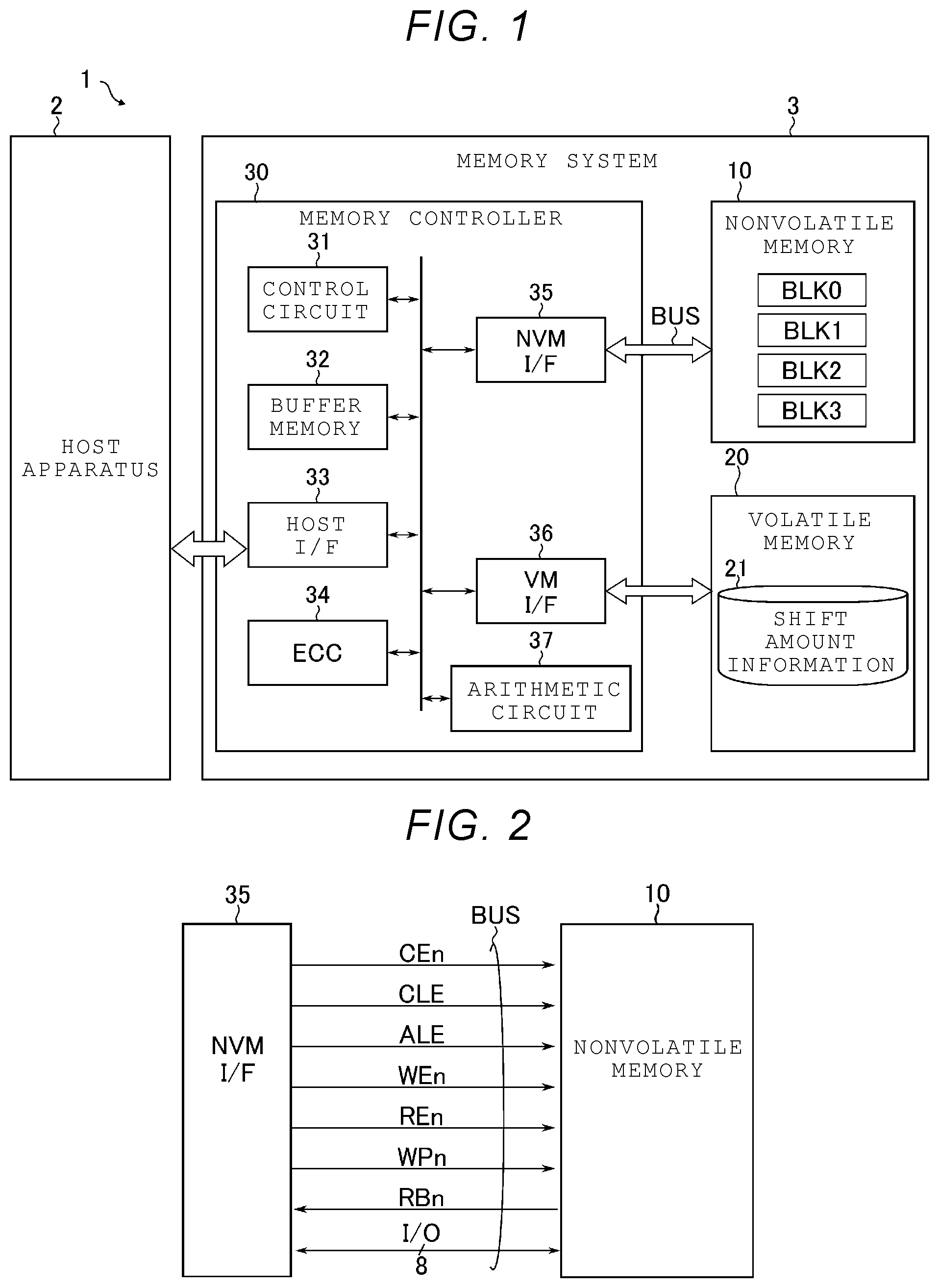
A configuration of an information processing system according to a first embodiment will be described. is a block diagram illustrating a configuration of the information processing system according to the first embodiment. As illustrated in , the information processing system 1 includes a host apparatus 2 and a memory system 3 .
The host apparatus 2 is a data processing apparatus that processes data using the memory system 3 . The host apparatus 2 is, for example, a personal computer or a server in a data center.
The memory system 3 is a storage device configured to be connected to the host apparatus 2 . The memory system 3 is, for example, a memory card such as an SD® card, a universal flash storage (UFS) device, or a solid state drive (SSD).
<1-1-2> Memory System
An internal configuration of the memory system according to the first embodiment will be described. The memory system 3 includes a nonvolatile memory 10 , a volatile memory 20 , and a memory controller 30 .
The nonvolatile memory 10 is, for example, a NAND flash memory. The nonvolatile memory 10 includes a plurality of blocks BLK (BLK 0 to BLK 3 ). Each of the blocks BLK includes a plurality of memory cell transistors (hereinafter, also simply referred to as memory cells) each of which stores data in a nonvolatile manner. Each of the blocks BLK is, for example, a unit of a data erase process.
The volatile memory 20 is, for example, a dynamic random access memory (DRAM). The volatile memory 20 stores shift amount information 21 . The details of the shift amount information 21 will be described below.
The memory controller 30 is configured with an integrated circuit such as a system-on-a-chip (SoC). The memory controller 30 controls the nonvolatile memory 10 based on a request from the host apparatus 2 or irrespective of a request from the host apparatus 2 .
Specifically, for example, the memory controller 30 reads data from the nonvolatile memory 10 based on a read request from the host apparatus 2 . The memory controller 30 transmits the read data to the host apparatus 2 . In addition, for example, the memory controller 30 reads data from the nonvolatile memory 10 as an internal process. The memory controller 30 controls the nonvolatile memory 10 based on the read data.
<1-1-3> Memory Controller
Next, an internal configuration of the memory controller 30 will be described with reference to . The memory controller 30 includes a control circuit 31 , a buffer memory 32 , a host interface circuit (host I/F) 33 , an error correction and check (ECC) circuit 34 , a nonvolatile memory interface circuit (NVM I/F) 35 , a volatile memory interface circuit (VM I/F) 36 , and an arithmetic circuit 37 . The function of each of the units 31 to 37 of the memory controller 30 described below may be implemented by any of dedicated hardware, a processor that executes firmware, or a combination thereof.
The control circuit 31 is a circuit that controls the entire memory controller 30 . The control circuit 31 includes, for example, a processor such as a central processing unit (CPU), and a read only memory (ROM).
The buffer memory 32 is, for example, a static random access memory (SRAM). The buffer memory 32 buffers data between the host apparatus 2 and the nonvolatile memory 10 . The buffer memory 32 temporarily stores write data and read data.
The host interface circuit 33 controls communication between the memory controller 30 and the host apparatus 2 . The host interface circuit 33 is connected to the host apparatus 2 via a host bus. The host bus is based on, for example, an SD® interface, an M-PHY, a serial attached small computer system interface (SAS), a serial advanced technology attachment (SATA), or a peripheral component interconnect express (PCIe®).
The ECC circuit 34 executes an error detection process and an error correction process regarding data stored in the nonvolatile memory 10 . That is, during a data write process, the ECC circuit 34 adds an error correction code to write data. During a data read process, the ECC circuit 34 decodes read data and detects whether a fail bit is included. The fail bit is a bit in data read from a plurality of memory cells that is different from data written therein. When the fail bit is detected, the ECC circuit 34 specifies a column address of the fail bit and executes error correction. Examples of a method of the error correction include hard decision decoding (also referred to as hard bit decoding) and soft decision decoding (also referred to as soft bit decoding). As a hard decision decoding code used for the hard decision decoding, for example, a Bose-Chaudhuri-Hocquenghem (BCH) code or a Reed-Solomon (RS) code may be used. As a soft decision decoding code used for the soft decision decoding, for example, a low density parity check (LDPC) code may be used.
The nonvolatile memory interface circuit 35 controls communication between the nonvolatile memory 10 and the memory controller 30 . The nonvolatile memory interface circuit 35 is connected to the nonvolatile memory 10 via a memory bus BUS. The memory bus BUS is based on, for example, a single data rate (SDR) interface, a toggle double data rate (DDR) interface, or an open NAND flash interface (ONFI).
The volatile memory interface circuit 36 controls communication between the volatile memory 20 and the memory controller 30 . A bus that connects the volatile memory 20 and the memory controller 30 is based on, for example, a DRAM interface specification.
The arithmetic circuit 37 is, for example, a counter. The arithmetic circuit 37 counts the number of memory cells that store the same value, based on read data stored in the buffer memory 32 .
<1-1-4> Memory Bus
Next, an example of a signal that is exchanged between the nonvolatile memory 10 and the memory controller 30 will be described. is a block diagram illustrating an example of signals that are used in the memory bus according to the first embodiment.
The signals used in the memory bus BUS include, for example, a chip enable signal CEn, a command latch enable signal CLE, an address latch enable signal ALE, a write enable signal WEn, a read enable signal REn, a write-protect signal WPn, a ready/busy signal RBn, and an input/output signal I/O. In the present specification, “n” at the end of a name of a signal represents that the signal is asserted when the level thereof is “low (L)”.
The chip enable signal CEn is a signal for enabling the nonvolatile memory 10 .
The command latch enable signal CLE and the address latch enable signal ALE are signals for notifying the nonvolatile memory 10 that signals I/O to the nonvolatile memory 10 are a command and an address, respectively.
The write enable signal WEn is a signal for inputting the signal I/O into the nonvolatile memory 10 .
The read enable signal REn is a signal for reading the signal I/O from the nonvolatile memory 10 .
The write-protect signal WPn is a signal for instructing the nonvolatile memory 10 to prevent data writing and erasing.
The ready/busy signal RBn is a signal representing whether the nonvolatile memory 10 is in a ready state or a busy state. The ready state is a state where the nonvolatile memory 10 can receive a command from the memory controller 30 . The busy state is a state where the nonvolatile memory 10 cannot receive a command from the memory controller 30 . The ready/busy signal RBn represents the busy state at the “L” level.
The input/output signal I/O is, for example, an 8-bit signal. The input/output signal I/O contains data that is transmitted and received between the nonvolatile memory 10 and the memory controller 30 . The input/output signal I/O includes a command, an address, a status, write data, and read data.
<1-1-5> Nonvolatile Memory
Next, an internal configuration of the nonvolatile memory 10 will be described. is a circuit diagram illustrating an example of a configuration of the nonvolatile memory according to the first embodiment. illustrates a configuration of the block BLK 0 as an example. Configurations of the other blocks BLK 1 to BLK 3 are the same as the configuration of the block BLK 0 . The block BLK 0 includes, for example, four string units SU 0 to SU 3 . In , the detailed configurations of the string units SU 2 and SU 3 are omitted.
Each of the string units SU includes a plurality of NAND strings NS that are associated with bit lines BL 0 to BLm (m represents an integer of 1 or larger), respectively. The NAND string NS include memory cell transistors MT 0 to MT 7 and select transistors ST 1 and ST 2 .
The memory cell transistor MT includes a control gate and a charge storage layer and stores data in a nonvolatile manner. Each of the select transistors ST 1 and ST 2 is used for selection of the string unit SU in various processes.
In each of the NAND strings NS, the memory cell transistors MT 0 to MT 7 are connected in series to each other. The select transistor ST 1 is connected between the associated bit line BL and one end of the memory cell transistors MT 0 to MT 7 that are connected in series. The drain of the select transistor ST 2 is connected to the other end of the memory cell transistors MT 0 to MT 7 that are connected in series. A source line SL is connected to the source of the select transistor ST 2 .
In the same block BLK, the gates of the plurality of select transistors ST 1 in each of the string units SU 0 to SU 3 are connected in common to each of select gate lines SGD 0 to SGD 3 . The control gates of the plurality of memory cell transistors MT 0 to MT 7 are connected in common to word lines WL 0 to WL 7 , respectively. The gates of the plurality of select transistors ST 2 are connected in common to a select gate line SGS.
The bit lines BL 0 to BLm are shared by the plurality of blocks BLK 0 to BLK 3 . The same bit line BL is connected to the NAND string NS corresponding to the same column address. The word lines WL 0 to WL 7 are provided in each of the blocks BLK 0 to BLK 3 . The source line SL is shared by, for example, the plurality of blocks BLK 0 to BLK 3 .
A group of a plurality of memory cell transistors MT that are connected to the common word line WL in one string unit SU will be referred to as, for example, “cell unit CU”, and is used as a unit of a data write process. For example, a storage capacity of the cell unit CU including the memory cell transistors MT each of which stores 1-bit data is defined as a page. The page is used as, for example, a unit of a data read process. In addition, data having a size corresponding to one page is defined as page data. That is, one page data is data having the same number of bits as the number of memory cell transistors MT in the cell unit CU. The cell unit CU may include a storage capacity of two or more pages according to the number of bits stored in the memory cell transistor MT.
The circuit configuration of the block BLK described above is merely exemplary, and the embodiment is not limited thereto. For example, the number of blocks BLK in the nonvolatile memory 10 may be any number according to the design. The number of the string units SU provided in each block BLK may be any number according to the design. The numbers of the memory cell transistors MT and the select transistors ST 1 and ST 2 in each of the NAND strings NS may be any numbers, respectively, according to the design.
In the embodiment, one memory cell transistor MT can store 3-bit data. That is, the memory cell transistor MT according to the embodiment is a triple level cell (TLC) that stores 3-bit data. Bits of the 3-bit data that is stored in the memory cell transistor MT configured as the TLC will be referred to as a lower bit, a middle bit, and an upper bit in order from the lowest bit. In addition, a group of the lower bits stored in the memory cell transistors MT in the same cell unit CU will be referred to as “lower page data, a group of the middle bits will be referred as “middle page data”, and a group of the upper bits will be referred as “upper page data”.
is a schematic diagram illustrating an example of threshold voltage distributions of the plurality of memory cell transistors MT, and an example of a cumulative distribution function, according to the first embodiment. The upper portion of illustrates the threshold voltage distribution, and the lower portion of illustrates the cumulative distribution function. When the memory cell transistor MT stores 3-bit data, the threshold voltage distribution is divided into eight sections. The eight threshold voltage distributions will be referred to as an “S0” state, an “S1” state, an “S2” state, an “S3” state, an “S4” state, an “S5” state, an “S6” state, and an “S7” state in order from the lowest threshold voltage.
In addition, each of voltages R 1 , R 2 , R 3 , R 4 , R 5 , R 6 , and R 7 illustrated in is used for distinguishing between two adjacent states during a data read process. A voltage VREAD is a voltage that is applied to a non-selected word line during the data read process. When the voltage VREAD is applied to the gate, the memory cell transistor MT enters an ON state irrespective of data stored therein. A relationship between the voltage values is R 1 <R 2 <R 3 <R 4 <R 5 <R 6 <R 7 <VREAD.
Among the threshold voltage distributions described above, the “S0” state corresponds to an erased state of the memory cell transistor MT. Threshold voltages in the “S0” state are lower than the voltage R 1 . Threshold voltages in the “S1” state are the voltage R 1 or higher and lower than the voltage R 2 . Threshold voltages in the “S2” state are the voltage R 2 or higher and lower than the voltage R 3 . Threshold voltages in the “S3” state are the voltage R 3 or higher and lower than the voltage R 4 . Threshold voltages in the “S4” state are the voltage R 4 or higher and lower than the voltage R 5 . Threshold voltages in the “S5” state are the voltage R 5 or higher and lower than the voltage R 6 . Threshold voltages in the “S6” state are the voltage R 6 or higher and lower than the voltage R 7 . Threshold voltages in the “S7” state are the voltage R 7 or higher and lower than the voltage VREAD.
The eight threshold voltage distributions are formed by writing 3-bit data including the lower bit, the middle bit, and the upper bit into each of the memory cell transistors MT. The eight threshold voltage distributions correspond to different pieces of 3-bit data. In the embodiment, data is assigned as “the upper bit/the middle bit/the lower bit” for a memory cell transistor MT in each of the states as described below.
That is, the memory cell transistor MT in the “S0” state stores “111” data. The memory cell transistor MT in the “S1” state stores “110” data. The memory cell transistor MT in the “S2” state stores “100” data. The memory cell transistor MT in the “S3” state stores “000” data. The memory cell transistor MT in the “S4” state stores “010” data. The memory cell transistor MT in the “S5” state stores “011” data. The memory cell transistor MT in the “S6” state stores “001” data. The memory cell transistor MT in the “S7” state stores “101” data.
A lower page read process is a data read process in which the voltage R 1 for distinguishing between the “S0” state and the “S1” state, and the voltage R 5 for distinguishing between the “S4” state and the “S5” state are used as the read voltages.
A middle page read process is a data read process in which the voltage R 2 for distinguishing between the “S1” state and the “S2” state, the voltage R 4 for distinguishing between the “S3” state and the “S4” state, and the voltage R 6 for distinguishing between the “S5” state and the “S6” state are used as the read voltages.
An upper page read process is a data read process in which the voltage R 3 for distinguishing between the “S2” state and the “S3” state, and the voltage R 7 for distinguishing between the “S6” state and the “S7” state are used as the read voltages.
Data stored in the cell unit CU is randomized such that the states including the “S0” state to the “S7” state” are uniformly present.
The cumulative distribution function illustrated in the lower portion of represents the number of memory cell transistors MT that are in an ON state when data is read using read voltages. The horizontal axis represents the read voltage, and the vertical axis represents the total number of memory cell transistors MT in the ON state (hereinafter, referred to as the number of ON-cells). It is assumed that an expected value of the number of memory cell transistors MT in each of the states is E. In this case, it is expected that, whenever the read voltage increases by an amount corresponding to the voltage for distinguishing between two states, the number of ON-cells increases by E.
Specifically, when the read voltage is the voltage R 1 , the expected value of the number of ON-cells is E. When the read voltage is increased up to the voltage R 2 , the expected value of the number of ON-cells is 2×E. When the read voltage is increased up to the voltage R 3 , the expected value of the number of ON-cells is 3×E. When the read voltage is increased up to the voltage R 4 , the expected value of the number of ON-cells is 4×E. When the read voltage is increased up to the voltage R 5 , the expected value of the number of ON-cells is 5×E. When the read voltage is increased up to the voltage R 6 , the expected value of the number of ON-cells is 6×E. When the read voltage is increased up to the voltage R 7 , the expected value of the number of ON-cells is 7×E. When the read voltage is increased up to the voltage VREAD, the expected value of the number of ON-cells is 8×E.
<1-1-6> Shift Amount Information
Next, a configuration of the shift amount information 21 will be described. is a diagram illustrating a configuration of the shift amount information used in the memory system according to the first embodiment. As illustrated in , the shift amount information 21 stores each of shift amounts (ΔR 1 _ i to ΔR 7 _ i ) of each of the read voltages R 1 to R 7 from a default value in association with a block BLKi.
The shift amount information 21 is used in an operation relating to the read voltage. For example, in a data read process, the memory controller 30 sets the read voltage based on the shift amount information 21 . For example, in a patrol process, the memory controller 30 determines a starting point of a shift amount search based on the shift amount information 21 . The details of the patrol process will be described below.
<1-2> Operation
Next, an operation of the memory system according to the first embodiment will be described.
<1-2-1> Shift Read Process and Tracking Process
First, a shift read process and a tracking process that are executed in the memory system 3 according to the first embodiment will be described. The shift read process and the tracking process are executed, for example, when it is assumed that a larger number of fail bits are detected at a default read voltage.
are schematic diagrams illustrating examples of the threshold voltage distributions of the plurality of memory cell transistors, and examples of the cumulative distribution function, according to the first embodiment. A and 6 B illustrate a state immediately after a data write process. A and 7 B illustrate a state where the adjacent threshold voltage distributions overlap each other.
As illustrated in A , for example, immediately after the data write process, threshold voltage distributions of an “S(n−1)” state (n represents an integer of 1 or larger and 7 or smaller) and an “Sn” state are separated from each other. Accordingly, the memory controller 30 can read correct data by setting the read voltage to a default read voltage Rndef between the threshold voltage distributions of the “S(n−1)” state and the “Sn” state.
B illustrates a relationship between the number of ON-cells and the read voltage immediately after the data write process. When the expected value of the number of memory cell transistors MT in each of the states is E, the voltage Rndef is a voltage close to an optimal read voltage at which the number of ON-cells is n×E.
However, the threshold voltage of the memory cell transistor MT may vary due to error factors such as disturbance or data retention. As a result, a distribution width of the threshold voltages in each of the states may spread, a mode of the threshold voltage distribution in each of the states may change, or the threshold voltage distribution in each of the states may shift. As a result of such changes of the threshold voltage distribution, as illustrated in A , the adjacent distributions may overlap each other. When the adjacent distributions overlap each other, data different from that during the data write process is read from the memory cell transistors MT, which corresponds to a thick oblique line portion and a thin oblique line portion in A . More specifically, among the memory cell transistors MT of the threshold voltage distribution in the “S(n−1)” state, read data of a memory cell transistor MT having a threshold voltage higher than or equal to the read voltage Rndef is a fail bit. In addition, among the memory cell transistors MT of the threshold voltage distribution in the “Sn” state, read data of a memory cell transistor MT having a threshold voltage lower than the read voltage Rndef is a fail bit. When the number of fail bits exceeds the number of correctable error bits of the ECC circuit 34 , data cannot be corrected.
When the read voltage can be appropriately shifted, the number of fail bits can be reduced. Examples of a method of determining the shift amount include a method of using the number of ON-cells. B illustrates a relationship between the number of ON-cells and the read voltage when the adjacent distributions overlap each other. By using a read voltage Rnopt at which the number of ON-cells is n×E, the number of fail bits can be reduced. Specifically, in A , by using the read voltage Rnopt, the number of fail bits can be reduced by the number of memory cell transistors MT corresponding to the thin oblique line portion, as compared to a case where the read voltage Rndef is used.
This way, a data read process that is executed by using, as the read voltage, a voltage shifted from the default read voltage by a certain voltage will be referred to as the shift read process. The shift amount information 21 described above is a group of shift amounts used for the shift read process.
In addition, an operation of searching for the shift amount used for the shift read process will be referred to as the tracking process.
The tracking process may be classified into a system tracking process that is executed by the memory controller 30 controlling the nonvolatile memory 10 and an on-chip tracking process that is executed by the nonvolatile memory 10 itself.
In the system tracking process, the memory controller 30 transmits a read command to the nonvolatile memory 10 such that the nonvolatile memory 10 executes a data read operation. The memory controller 30 receives read data from the nonvolatile memory 10 and searches for the shift amount based on the read data.
In the system tracking process, the memory controller 30 searches for the shift amount. As a result, a complex and high-level tracking process can be executed.
On the other hand, in the on-chip tracking process, the memory controller 30 transmits an on-chip tracking command and a shift amount to the nonvolatile memory 10 . The nonvolatile memory 10 that receives the on-chip tracking command and the shift amount executes a data read operation, and searches for a more suitable shift amount based on the read data, for example from the shift amount received as a starting point. When the search of the shift amount ends, the nonvolatile memory 10 transmits the shift amount information to the memory controller 30 .
The on-chip tracking process is executed by the nonvolatile memory 10 alone except for exchanging the command and the result. As a result, the tracking process can be executed within a short period of time.
<1-2-2> Patrol Operation
The memory system 3 according to the first embodiment executes the patrol process, for example, in a period where a command from the host is not executed. The patrol process includes the tracking process and the shift read process. The details of the patrol process will be described.
is a flowchart illustrating an example of the patrol process in the memory system according to the first embodiment.
When the patrol process starts (START), the memory controller 30 acquires the shift amount information 21 (S 10 ). Specifically, the memory controller 30 reads the shift amount information 21 from the volatile memory 20 .
The memory controller 30 executes the tracking process (S 11 ). Specifically, the memory controller 30 executes the tracking process based on the acquired shift amount information 21 . The tracking process is a process of reading data from the nonvolatile memory 10 and searching for a new shift amount. The details of the tracking process will be described below. As a result of the tracking process, the memory controller 30 acquires the newly obtained shift amount information.
The memory controller 30 causes the nonvolatile memory 10 to execute a data read process (S 12 ). Specifically, the memory controller 30 causes the nonvolatile memory 10 to execute the data read process using the shift amount information acquired in the tracking process. As a result of executing the data read process, the memory controller 30 acquires the read data.
In Step S 13 , the ECC circuit 34 of the memory controller 30 executes hard decision decoding on the data acquired in the data read process.
The memory controller 30 determines whether the decoding is successful (S 14 ).
When the decoding is successful (S 14 , Yes), the memory controller 30 updates the shift amount information 21 (S 15 ). Specifically, the memory controller 30 updates the shift amount information 21 in the volatile memory 20 such that the default shift amount information 21 is overwritten with the shift amount information acquired in the process of Step S 11 . The patrol process ends (END).
When the decoding is not successful (S 14 , No), the patrol process ends (END).
Next, the details of the tracking process will be described. The tracking process is a process of searching for a suitable shift amount for each of the read voltages R 1 to R 7 . In order to simplify the description, a case of searching for the shift amount for a read voltage Rn will be described as an example, where n represents an integer of 1 or larger and 7 or smaller.
are flowcharts illustrating an example of the tracking process in the memory system according to the first embodiment.
When the tracking process starts (START), the memory controller 30 determines an initial value of the shift amount (S 20 ). Specifically, the initial value shift int of the shift amount is calculated using the following Expression (1).
shift int = shift hold - ( ( SP - 1 ) × ST ÷ 2 ) ( 1 )
In Expression (1), shift hold represents the shift amount read from the shift amount information 21 , SP represents the number of times of sampling, and ST represents a search step. The number of times of sampling SP is an integer of 2 or larger, and the search step ST is a voltage other than 0.
Expression (1) will be described. is a diagram illustrating Expression (1). The memory system 3 according to the first embodiment searches for the suitable shift amount in the voltage range of (SP−1)×ST, around the shift amount shift hold . Therefore, the initial value shift int of the shift amount is set to a voltage lower than the shift amount shift hold by ((SP−1)×ST=2).
Referring back to , the memory controller 30 resets a variable “i” to 1 (S 21 ).
The memory controller 30 causes the nonvolatile memory 10 to execute a data read process using “shift (i)” as the shift amount (S 22 ). Specifically, the “shift (i)” is represented by the following Expression (2).
shift ( i ) = shift int + ( i - 1 ) × ST ( 2 )
The data read process is executed, for example, on one cell unit CU of one block BLK. As a result of causing the nonvolatile memory 10 to execute the data read process, the memory controller 30 acquires the read data.
Expression (2) will be described. is a diagram illustrating Expression (2). In the memory system 3 according to the first embodiment, shift(1) is the same as shift int . In addition, when i is 2 or larger, shift (i) is set to a voltage that is increased by ST whenever i increases by 1. In addition, a difference between shift(1) and shift (SP) is (SP−1)×ST that is the same as the search range.
Referring back to , the arithmetic circuit 37 of the memory controller 30 calculates the number of ON-cells “chist(i)” (S 23 ). Specifically, the arithmetic circuit 37 of the memory controller 30 counts the number of ON-cells in the data read process using “shift (i)” as the shift amount, and calculates the counted number as “chist(i)”. Further, the memory controller 30 stores the calculated number of ON-cells “chist(i)” in the volatile memory 20 .
The memory controller 30 increments the variable “i” (S 24 ).
The memory controller 30 determines whether the variable “i” is larger than the number of times of sampling SP (S 25 ). When the variable “i” is not larger than the number of times of sampling SP (S 25 , No), the process of Step S 22 is executed. That is, while the variable “i” is the number of times of sampling SP or smaller, the data read process using “shift (i)” corresponding to the incremented variable “i” is executed.
When the variable “i” is larger than the number of times of sampling SP (S 25 , Yes), as illustrated in , the memory controller 30 resets the variable “i” to 1 (S 26 ).
The memory controller 30 determines whether the number of ON-cells “chist(i)” is smaller than an expected value “chist exp ” (S 27 ). When the expected value of the number of memory cell transistors MT in each of the states is E and the read voltage Rn is a search target of the shift amount, the expected value “chist exp ” is E×n.
When the number of ON-cells “chist(i)” is smaller than the expected value “chist exp ” (S 27 , Yes), the memory controller 30 increments the variable “i” (S 28 ).
The memory controller 30 determines whether the variable “i” is larger than the number of times of sampling SP (S 29 ). When the variable “i” is not larger than the number of times of sampling SP (S 29 , No), the process of Step S 27 is executed.
That is, while the variable “i” is the number of times of sampling SP or smaller, the number of ON-cells “chist(i)” corresponding to the incremented variable “i” and the expected value “chist exp ” are compared to each other. As a result, among the incremented values of the variable “i” with which the number of ON-cells “chist(i)” is larger than the expected value “chist exp ”, the minimum value of the variable “i” is acquired.
When the variable “i” is larger than the number of times of sampling SP (S 29 , Yes), the initial value of the shift amount is changed (S 30 ), and the process of Step S 21 is executed. Specifically, (SP−1)×ST is added to shift int , and the process of Step S 21 is executed.
That is, in the previous search range, the number of ON-cells “chist(i)” that is larger than the expected value “chist exp ” was not acquired. Therefore, the initial value of the shift amount is changed such that the search can be performed with a higher voltage (S 30 ). is a diagram illustrating the initial value of the shift amount that is changed in Step S 30 . As illustrated in , (SP−1)×ST is added to the previous shift int . As a result, the initial value of the shift amount is changed such that the end point of the previous search becomes a starting point of a new search.
Referring back to , in the process of Step S 27 , when the number of ON-cells “chist(i)” is not smaller than the expected value “chist exp ” (S 27 , No), the memory controller 30 determines whether the variable “i” is 1 (S 31 ). The reason for this is as follows. When the variable “i” is 1, the number of ON-cells “chist(1)” at the starting point of the search is larger than the expected value “chist exp ”. That is, this case shows that the search range is excessively high.
When the variable “i” is 1 (S 31 , Yes), the initial value of the shift amount is changed (S 32 ), and the process of Step S 21 is executed. Specifically, (SP−1)× ST is subtracted from shift int , and the process of Step S 21 is executed.
That is, in the previous search range, the number of ON-cells “chist(i)” that is smaller than the expected value “chist exp ” was not acquired. Therefore, the initial value of the shift amount is changed such that the search can be performed with a lower voltage (S 32 ). is a diagram illustrating the initial value of the shift amount that is changed in Step S 32 . As illustrated in , (SP−1)×ST is subtracted from the previous shift int . As a result, the initial value of the shift amount is changed such that the starting point of the previous search is an end point of a new search.
Referring back to , it can be seen that, when the determination of Step S 27 is No and the determination of Step S 31 is No, the number of ON-cells “chist(i)” at a voltage other than the starting point of the search range exceeds the expected value “chist exp ”. That is, two values of the variable “i” (that is, the current value “i” and the value “i−1”) corresponding to two numbers of ON-cells “chist(i)” between which the expected value “chist exp ” is interposed are acquired. As a result, the memory controller 30 can determine the suitable shift amount.
When the variable “i” is not 1 (S 31 , No), the memory controller 30 determines the suitable shift amount (S 33 ). Specifically, the suitable shift amount is calculated from the following Expression (3).
shift opt = shift ( i - 1 ) + ST × ( chist exp - chist ( i - 1 ) ) ÷ ( chist ( i ) - chist ( i - 1 ) ) ( 3 )
During the calculation, the memory controller 30 reads the number of ON-cells “chist(i−1)” from the volatile memory 20 .
Expression (3) will be described. is a diagram illustrating Expression (3). Since the numbers of ON-cells “chist(i−1)” and “chist(i)” and the expected value “chist exp ” are known, the memory controller 30 can acquire the number of ON-cells between “chist(i−1)” and “chist(i)” and the number of ON-cells between “chist(i−1)” and “chist exp ”. Using these results, the memory controller 30 can acquire an internal ratio between the distributions of the numbers of ON-cells [(chist exp −chist(i−1))÷(chist(i)−chist(i−1))]. By multiplying this internal ratio by the search step ST and adding the result of the multiplication to the shift amount “shift(i−1)”, the memory controller 30 can calculate the suitable shift amount “shift opt ”.
Referring back to , when the suitable shift amount is determined (S 33 ), a series of processes ends (END). As described above with reference to , the memory controller 30 executes the data read process (S 12 ) and the hard decision process (S 13 ) using the shift amount determined in the tracking process. When the decoding is successful (S 14 , Yes), the default shift amount information 21 is overwritten with the shift amount.
<1-2-3> Host Read Operation
The details of a host read process will be described. The host read process is a data read process that is executed based on a read request from the host apparatus.
is a flowchart illustrating an example of the host read process in the memory system according to the first embodiment.
When the read request is received from the host apparatus 2 (START), the memory controller 30 acquires the shift amount information 21 (S 40 ). Specifically, the memory controller 30 reads the shift amount information 21 from the volatile memory 20 .
The memory controller 30 causes the nonvolatile memory 10 to execute a data read process (S 41 ). Specifically, the memory controller 30 causes the nonvolatile memory 10 to execute the data read process using the shift amount stored in the shift amount information 21 . As a result of executing the data read process, the memory controller 30 acquires read data.
In Step S 42 , the ECC circuit 34 of the memory controller 30 executes hard decision decoding on the data acquired in the data read process.
The memory controller 30 determines whether the decoding is successful (S 43 ). When the decoding is successful (S 43 , Yes), the memory controller 30 transmits the decoded read data to the host apparatus 2 , and ends the host read process (END).
When the decoding is not successful (S 43 , No), the memory controller 30 causes the nonvolatile memory 10 to execute the on-chip tracking process (S 44 ). Specifically, the memory controller 30 transmits the shift amount information 21 acquired in the process of Step S 40 and an on-chip tracking command to the nonvolatile memory 10 , and causes the nonvolatile memory 10 to execute the on-chip tracking process. Shift amount information acquired in the on-chip tracking process is transmitted from the nonvolatile memory 10 to the memory controller 30 .
The memory controller 30 causes the nonvolatile memory 10 to execute a data read process (S 45 ). Specifically, the memory controller 30 causes the nonvolatile memory 10 to execute the data read process using the received shift amount information. As a result of executing the data read process, the memory controller 30 acquires read data.
In Step S 46 , the ECC circuit 34 of the memory controller 30 executes hard decision decoding on the data acquired in the data read process.
The memory controller 30 determines whether the decoding is successful (S 47 ). When the decoding is not successful (S 47 , No), the memory controller 30 causes the nonvolatile memory 10 to execute a data read process (S 48 ). Specifically, the memory controller 30 causes the nonvolatile memory 10 to execute a data read process for the soft decision decoding. As a result of executing the data read process, the memory controller 30 acquires read data.
In Step S 49 , the ECC circuit 34 of the memory controller 30 executes the soft decision decoding on the data acquired in the data read process.
The memory controller 30 determines whether the decoding is successful (S 50 ). When the decoding is not successful (S 50 , No), the memory controller 30 reports error to the host apparatus 2 (S 51 ). Specifically, the memory controller 30 reports uncorrectable error to the host apparatus 2 . The host read process ends (END).
When the decoding is successful in the process of Step S 47 or Step S 50 (S 47 or S 50 , Yes), the memory controller 30 updates the shift amount information 21 (S 52 or S 53 ). Specifically, the memory controller 30 updates the shift amount information 21 in the volatile memory 20 such that the default shift amount information 21 is overwritten with the shift amount information acquired in the process of Step S 44 . The decoded read data is transmitted to the host apparatus 2 , and the host read process ends (END).
<1-3> Effect
In the memory system according to the first embodiment described above, the operating speed can be improved.
The memory system according to the first embodiment executes the tracking process irrespective of a request from the host apparatus, executes a data read process using the acquired shift amount information, and updates the shift amount information 21 when error correction is successful. That is, the memory system according to the first embodiment can update the shift amount information 21 such that the current state of the nonvolatile memory 10 is reflected. The memory system according to the first embodiment executes the on-chip tracking process based on the shift amount information 21 when error correction of read data fails in the host read process. As a result, the memory system according to the first embodiment can rapidly search for more suitable shift amount information. Accordingly, the memory system according to the first embodiment can improve the operating speed.
<2> Second Embodiment
A configuration of a memory system according to a second embodiment is different from the memory system of the first embodiment in the configuration of the volatile memory 20 and the tracking process. Hereinafter, regarding the memory system according to the second embodiment, points different from the first embodiment will be described.
<2-1> Configuration
<2-1-1> Memory System
is a block diagram illustrating a configuration of an information processing system according to the second embodiment. In the memory system 3 according to the second embodiment, the volatile memory 20 further stores a lookup table (LUT) 22 as compared to the memory system 3 according to the first embodiment.
is a diagram illustrating an example of a configuration of the lookup table used in the memory system according to the second embodiment. As illustrated in , the LUT 22 stores differences in the number of ON-cells ΔC 1 , ΔC 2 , ΔC 3 , . . . and amounts of change in read voltage ΔVR 1 , ΔVR 2 , ΔVR 3 , . . . . The LUT 22 is used in the tracking process. The LUT 22 associates the difference in the number of ON-cells and the amount of change in read voltage with each other. This association is experimentally acquired, for example, before the shipping of the memory system 3 . For example, when the number of ON-cells is desired to be increased by a certain number, the memory controller 30 can learn the amount of change in read voltage corresponding to the certain number by referring to the LUT 22 . The LUT 22 may associate the difference in the number of ON-cells and the amount of change in read voltage with each other for each of the read voltages R 1 to R 7 . The LUT 22 may further associate the difference in the number of ON-cells and the amount of change in read voltage with each other for each of the blocks.
<2-2> Operation
Next, an operation of the memory system according to the second embodiment will be described. The details of the tracking process will be described. In order to simplify the description, a case of searching for the shift amount for a read voltage Rn will be described as an example. Here, “n” represents an integer of 1 or larger and 7 or smaller.
are flowcharts illustrating an example of the tracking process in the memory system according to the second embodiment.
When the tracking process starts (START), the memory controller 30 determines a shift amount “shift” from the shift amount information 21 (S 60 ). Specifically, the memory controller 30 determines, from the shift amount information 21 , the shift amount “shift” based on a block BLK that includes a memory cell transistor MT for which the shift amount is to be searched, and a read voltage at which the shift amount is to be searched.
The memory controller 30 causes the nonvolatile memory 10 to execute a data read process using “shift” as the shift amount (S 61 ). The data read process is executed, for example, on one cell unit CU of one block BLK. As a result of causing the nonvolatile memory 10 to execute the data read process, the memory controller 30 acquires read data.
The arithmetic circuit 37 of the memory controller 30 calculates the number of ON-cells “chist(shift)” (S 62 ). Specifically, the arithmetic circuit 37 of the memory controller 30 counts the number of ON-cells in the data read process using “shift” as the shift amount, and calculates the counted number as “chist(shift)”.
The memory controller 30 determines whether the number of ON-cells “chist(shift)” is smaller than the expected value “chist exp ” (S 63 ). When the number of ON-cells “chist(shift)” is smaller than the expected value “chist exp ” (S 63 , Yes), the memory controller 30 sets 1 into a variable “sign” (S 64 ).
When the number of ON-cells “chist(shift)” is not smaller than the expected value “chist exp ” (S 63 , No), the memory controller 30 sets −1 into the variable “sign” (S 65 ).
This way, 1 or −1 is set into the variable “sign” based on a magnitude relationship between the number of ON-cells “chist(shift)” and the expected value “chist exp ”.
The memory controller 30 determines a differential shift amount “val” from the LUT 22 (S 66 ). Specifically, the memory controller 30 refers to the LUT 22 to determine the differential shift amount “val” from a difference between the number of ON-cells “chist(shift)” and the expected value “chist exp ”.
The memory controller 30 stores each of the values of the shift amount “shift”, the number of ON-cells “chist(shift)”, and the variable “sign” (S 67 ). More specifically, the memory controller 30 sets the shift amount “shift” into a shift amount “shift pre ”, sets the number of ON-cells “chist(shift)” into the number of ON-cells “chist pre ”, and sets the variable “sign” into a variable “sign pre ” (S 67 ).
The memory controller 30 adds a value obtained by multiplying the variable “sign” by the differential shift amount “val” to the shift amount “shift” (S 68 ).
To the variable “sign”, 1 or −1 is set based on a magnitude relationship between the number of ON-cells “chist(shift)” and the expected value “chist exp ”. Therefore, the process of Step S 68 is a process of adding or subtracting the differential shift amount “val” to or from the shift amount “shift”. Specifically, when the number of ON-cells “chist(shift)” is smaller than the expected value “chist exp ”, the process of Step S 68 is the addition. That is, the shift amount “shift” is set to a value increased by the differential shift amount “val” such that the number of ON-cells “chist(shift)” increases. On the other hand, when the number of ON-cells “chist(shift)” is not smaller than the expected value “chist exp ”, the process of Step S 68 is the subtraction. That is, the shift amount “shift” is set to a value decreased by the differential shift amount “val” such that the number of ON-cells “chist(shift)” decreases.
As illustrated in , the memory controller 30 causes the nonvolatile memory 10 to execute a data read process using “shift” as the shift amount (S 69 ). As a result of causing the nonvolatile memory 10 to execute the data read process, the memory controller 30 acquires read data.
The arithmetic circuit 37 of the memory controller 30 calculates the number of ON-cells “chist(shift)” (S 70 ).
The memory controller 30 determines again whether the number of ON-cells “chist(shift)” is smaller than the expected value “chist exp ” (S 71 ). When the number of ON-cells “chist(shift)” is smaller than the expected value “chist exp ” (S 71 , Yes), the memory controller 30 sets 1 into the variable “sign” (S 72 ).
When the number of ON-cells “chist(shift)” is not smaller than the expected value “chist exp ” (S 71 , No), the memory controller 30 sets −1 into the variable “sign” (S 73 ).
The memory controller 30 determines whether the value obtained by multiplying the variable “sign pre ”, which is stored in Step S 67 , by the variable “sign”, into which the value is set in Step S 72 or Step S 73 , is smaller than 0 (S 74 ). When the value obtained by multiplying the variable “sign pre ” and the variable “sign” is smaller than 0 (S 74 , Yes), the process of Step S 75 is executed. When the value obtained by multiplying the variable “sign pre ” and the variable “sign” is not smaller than 0 (S 74 , No), the process of Step S 67 is executed.
In Step S 74 , the memory controller 30 determines whether a first magnitude relationship between the number of ON-cells “chist(shift)” and the expected value “chist exp ” and a second magnitude relationship between the number of ON-cells “chist pre ” and the expected value “chist exp ” are different from each other.
Specifically, when the magnitude relationships are different from each other, the multiplication result of the variable “sign pre ” and the variable “sign” is −1. This case shows that the expected value “chist exp ” is present between the numbers of ON-cells “chist pre ” and “chist(shift)”. That is, two shift amounts (that is, the current value “shift” and the value “shift pre ”) corresponding to two numbers of ON-cells between which the expected value “chist exp ” is interposed are acquired. In this case, the determination of Step S 74 is Yes, and the process of Step S 75 is executed.
On the other hand, when the magnitude relationships are the same as each other, the multiplication result of the variable “sign pre ” and the variable “sign” is 1. This case shows that the expected value “chist exp ” is larger than the numbers of ON-cells “chist pre ” and “chist(shift)” or that the expected value “chist exp ” is smaller than the numbers of ON-cells “chist pre ” and “chist(shift)”. In this case, the determination of Step S 74 is No, and the process of Step S 67 is executed again. In the next Step S 68 , the addition or the subtraction of the differential shift amount “val” is executed.
The memory controller 30 determines whether the differential shift amount “val” is a threshold TH or smaller (S 75 ). When the differential shift amount “val” is not the threshold TH or smaller (S 75 , No), the memory controller 30 divides the differential shift amount “val” by 2 (S 76 ), and executes the process of Step S 67 again.
In Step S 75 , the memory controller 30 determines whether the differential shift amount “val” that is an interval between the shift amounts “shift pre ” and “shift” is the threshold TH or smaller. In the calculation of the shift amount described below, when the differential shift amount “val” is large, the calculation may have relatively large error. Therefore, the memory controller 30 checks whether the sufficient small differential shift amount “val” is acquired. That is, when the differential shift amount “val” is the threshold TH or smaller, the process proceeds to Step S 77 . Otherwise, the process of Step S 76 is executed, and the processes after Step S 67 are executed again using the differential shift amount “val” divided by 2.
When the differential shift amount “val” is the threshold TH or smaller (S 75 , Yes), the memory controller 30 determines the suitable shift amount (S 77 ). Specifically, the memory controller 30 calculates the suitable shift amount from the following Expression (4). shift opt =shift pre +(shift−shift pre )×(chist exp −chist pre )÷(chist(shift)−chist pre ) (4)
The series of processes end (END).
Expression (4) will be described. is a diagram illustrating Expression (4). Since the numbers of ON-cells “chist pre ” and “chist(shift)” and the expected value “chist exp ” are known, the memory controller 30 can acquire the number of ON-cells between “chist(shift)” and “chist pre ” and the number of ON-cells between “chist(shift)” and “chist exp ”. Using these results, the memory controller 30 can acquire an internal ratio between the distributions of the numbers of ON-cells [(chist exp −chist pre )÷(chist(shift)−chist pre )]. By multiplying this internal ratio by a difference between the shift amounts “shift” and “shift pre ” and adding the multiplication result to the shift amount “shift pre ”, the memory controller 30 can calculate the suitable shift amount “shift opt ”.
Regarding the tracking process in the memory system according to the second embodiment, an operation will be described in detail using a specific example. is a diagram illustrating the specific example of the tracking process in the memory system according to the second embodiment. In , the process of Step S 68 described with reference to is indicated by arrows. In addition, the value of the variable “sign” at each of read voltages is added with parentheses. In addition, when the read voltage is higher than a voltage indicated by a broken line, it is assumed that the number of ON-cells “chist(shift)” exceeds the expected value “chist exp ”. In addition, it is assumed that the threshold TH is S/3.
In the example illustrated in , a read voltage VA is determined using the shift amount “shift” from the shift amount information 21 (S 60 of ). At the read voltage VA, the number of ON-cells “chist(shift)” is smaller than the expected value “chist exp ”, and thus the variable “sign” is 1. A voltage S as the differential shift amount “val” is determined (S 66 of ).
The voltage S is added to the voltage VA, and a read voltage based on the new shift amount is a voltage VB (S 68 of ). Even at the read voltage VB, the number of ON-cells “chist(shift)” is smaller than the expected value “chist exp ”, and thus the variable “sign” is 1. Since both of the variables “sign pre ” (that is, the variable “sign” corresponding to the read voltage VA) and “sign” are 1 (S 74 of , No), the read voltage based on the new shift amount is determined again.
The voltage S is added to the voltage VB, and a read voltage based on the new shift amount is a voltage VC (S 68 of ). Even at the read voltage VC, the number of ON-cells “chist(shift)” is smaller than the expected value “chist exp ”, and thus the variable “sign” is 1. Since both of the variables “sign pre ” (that is, the variable “sign” corresponding to the read voltage VB) and “sign” are 1 (S 74 of , No), the read voltage based on the new shift amount is determined again.
The voltage S is added to the voltage VC, and a read voltage based on the new shift amount is a voltage VD (S 68 of ). At the read voltage VD, the number of ON-cells “chist(shift)” is larger than the expected value “chist exp ”, and thus the variable “sign” is −1. Since the variable “sign pre ” (that is, the variable “sign” corresponding to the read voltage VC) is 1 and the variable “sign” is −1 (S 74 of , Yes), the size of the differential shift amount is determined (S 75 of ). Since the voltage S as the differential shift amount is larger than the threshold TH (S 75 of , No), the differential shift amount is divided by 2 (S 76 of ). The differential shift amount is now S/2, and the read voltage based on the new shift amount is determined again.
The voltage S/2 is subtracted from the voltage VD, and a read voltage based on the new shift amount is a voltage VE (S 68 of ). At the read voltage VE, the number of ON-cells “chist(shift)” is larger than the expected value “chist exp ”, and thus the variable “sign” is −1. Since both of the variables “sign pre ” (that is, the variable “sign” corresponding to the read voltage VD) and “sign” are −1 (S 74 of , No), the read voltage based on the new shift amount is determined again.
The voltage S/2 is subtracted from the voltage VE, and a read voltage based on the new shift amount is a voltage VF (S 68 of ). At the read voltage VF, the number of ON-cells “chist(shift)” is smaller than the expected value “chist exp ”, and thus the variable “sign” is 1. Since the variable “sign pre ” (that is, the variable “sign” corresponding to the read voltage VE) is −1 and the variable “sign” is 1 (S 74 of , Yes), the size of the differential shift amount is determined again (S 75 of ). Since the voltage S/2 as the differential shift amount is larger than the threshold TH (S 75 of , No), the differential shift amount is divided by 2 (S 76 of ). The differential shift amount is now S/4, and the read voltage based on the new shift amount is determined again.
The voltage S/4 is added to the voltage VF, and a read voltage based on the new shift amount is a voltage VG (S 68 of ). At the read voltage VG, the number of ON-cells “chist(shift)” is smaller than the expected value “chist exp ”, and thus the variable “sign” is 1. Since both of the variables “sign pre ” (that is, the variable “sign” corresponding to the read voltage VF) and “sign” are 1 (S 74 of , No), the read voltage based on the new shift amount is determined again.
The voltage S/4 is added to the voltage VG, and a read voltage based on the new shift amount is a voltage VH (S 68 of ). At the read voltage VH, the number of ON-cells “chist(shift)” is larger than the expected value “chist exp ”, and thus the variable “sign” is −1. Since the variable “sign pre ” (that is, the variable “sign” corresponding to the read voltage VG) is 1 and the variable “sign” is −1 (S 74 of , Yes), the size of the differential shift amount is determined again (S 75 of ). Since the voltage S/4 as the differential shift amount is smaller than the threshold TH (S 75 of , Yes), the suitable shift amount is determined (S 77 of ). That is, the suitable shift amount “shift opt ” is calculated using the read voltage VG and the read voltage VH.
In this way, the memory system according to the second embodiment calculates the suitable shift amount “shift opt ” by increasing or decreasing the shift amount while decreasing the additional shift amount “val”.
<2-3> Effect
In the memory system according to the second embodiment described above, the operating speed can be improved.
The memory system according to the second embodiment determines a read voltage at the starting point based on the shift amount information 21 in the tracking process, and reads a plurality of pieces of data while decreasing the shift amount from the starting point, and determines the suitable shift amount. The memory system according to the second embodiment can rapidly search for the suitable shift amount by narrowing the search step from a large shift amount to a small shift amount. As a result, the memory system according to the second embodiment can improve the operating speed.
<3> Modification Examples
When the search range is inappropriate, the memory system according to the first embodiment changes the initial value of the shift amount (S 30 and S 32 of ), and searches for the suitable shift amount in a new search range (S 21 and thereafter of ). However, when the search range is inappropriate, the memory system may calculate the shift amount and end the process. Specifically, instead of the processes of Step S 30 and thereafter described with reference to , the memory system may calculate a shift amount “shift(SP)” as “shift opt ” and end the process. In addition, instead of the processes of Step S 32 and thereafter described with reference to , the memory system may calculate a shift amount “shift(1)” as “shift opt ” and end the process.
In the embodiment described above, the division is executed. The memory system may round up or round down the result of the division.
In the embodiment described above, the two examples of the tracking process (S 11 of ) are described. However, the tracking process is not limited to the examples described in the embodiment described above, and various modifications can be made. For example, hereinafter, a first estimation method will be described.
(First Estimation Method)
In the first estimation method, the memory controller 30 causes the nonvolatile memory 10 to execute a plurality of data read processes while shifting the read voltage. The arithmetic circuit 37 calculates, as a histogram H 1 , the number of memory cell transistors MT in each of threshold voltage ranges, which are divided by a plurality of read voltages, based on a plurality of pieces of read data acquired by the plurality of data read processes. The number of memory cell transistors MT in each of threshold voltage ranges is referred to as the number of interval cells.
The control circuit 31 determines the plurality of read voltages R 1 to R 7 based on the calculated histogram H 1 . The control circuit 31 calculates a plurality of shift amounts ΔR 1 to ΔR 7 based on the determined plurality of read voltages R 1 to R 7 . A method of determining the plurality of read voltages R 1 to R 7 based on the histogram H 1 will be described using A to 23 C .
A to 23 C are diagrams illustrating an example of the first estimation method that is applied to a shift amount estimation process in the memory system according to the modification example.
A illustrates, for example, two threshold voltage distributions corresponding to the “S0” state and the “S1” state. B illustrates the transition of the number of ON-cells M. C illustrates the transition of the amount of change in the number of ON-cells between two read voltages, that is, the number of interval cells C. C corresponds to the histogram H 1 described above.
As illustrated in B , as the read voltage V is shifted from a higher voltage side to a lower voltage side, the number of ON-cells M rapidly decreases at a voltage that is slightly higher than a voltage VS 1 mid, which is a mode of the “S1” state, and |dM/dV| is the maximum. Here, the mode is a voltage at which the distribution probability of the threshold voltage in A is the maximum. Further, as the read voltage V decreases, the decrease rate of the number of ON-cells M decreases, and the decrease rate of the number of ON-cells M at a certain value of the read voltage V is the minimum. When the threshold voltage distribution belonging to the “S1” state and the threshold voltage distribution belonging to the “S0” state do not overlap each other, the minimum value of the decrease rate of the number of ON-cells M is zero. On the other hand, when the threshold voltage distribution belonging to the “S1” state and the threshold voltage distribution belonging to the “S0” state overlap each other, the minimum value of the decrease rate of the number of ON-cells M is a value (>0) other than zero. As the read voltage V further decreases, the decrease rate of the number of ON-cells M further increases, and |dM/dV| is the maximum again at a voltage that is slightly higher than a voltage VS 0 mid, which is a mode of the “S0” state.
A read voltage V at which the overlapping of the threshold voltage distributions between two states is the minimum (that is, the read voltage V corresponding to an intersection between the threshold voltage distributions of the two states) can be detected by the change in the number of ON-cells M described above. For example, first, the memory system according to the modification example executes a data read process using a read voltage V 0 . At this time, the number of ON-cells is M 0 . Next, the memory system executes a data read process using a voltage V 1 that is lower than the voltage V 0 by ΔV. At this time, the number of ON-cells is M 1 . As a result, when the read voltage is decreased from V 0 to V 1 , the number of memory cell transistors MT that newly enter an OFF state is C 1 =M 0 −M 1 . That is, the number of interval cells in a threshold voltage range [V 0 ,V 1 ] is C 1 .
Next, the memory system executes a data read process using a voltage V 2 that is lower than the voltage V 1 by ΔV. At this time, the number of ON-cells is M 2 . As a result, when the read voltage is decreased from V 1 to V 2 , the number of memory cell transistors MT that newly enter an OFF state is C 2 =M 1 −M 2 . That is, the number of interval cells in a threshold voltage range [V 1 ,V 2 ] is C 2 . Assuming that C 1 >C 2 , it is considered that a voltage at which |dM/dV| is the minimum is positioned at least on a lower voltage side than the voltage V 1 .
Next, the memory system executes a data read process using a voltage V 3 that is lower than the voltage V 2 by ΔV. At this time, the number of ON-cells is M 3 . As a result, when the read voltage is decreased from V 2 to V 3 , the number of memory cell transistors MT that newly enter an OFF state is C 3 =M 2 −M 3 . That is, the number of interval cells in a threshold voltage range [V 2 ,V 3 ] is C 3 . Here, assuming that C 3 >C 2 , the histogram shown in C is acquired as the histogram H 1 .
As a result, the threshold voltage distribution indicated by a chain line in C can be estimated based on the numbers of interval cells C. It can be estimated that a read voltage at which the overlapping of the threshold voltage distribution belonging to the “S1” state and the threshold voltage distribution belonging to the “S0” state is the minimum is present between the voltage V 1 and the voltage V 2 (in the interval where the number of interval cells is the minimum value).
Through the operation described above, in the first estimation method, the read voltage is determined based on the plurality of data read processes.
When data stored in each of the memory cell transistors MT is associated with non-continuous voltage ranges, a data read process of one page data (also referred to as page read process) may include data read processes using a plurality of read voltages. Specifically, for example, as described above with reference to , data of “1” of the lower bit is associated with a voltage range of the read voltage R 1 or lower (that is the “S0” state) and a voltage range of the read voltage R 5 or higher (that is, the “S5” to “S7” states). Therefore, only with read data acquired by the lower page read process (that is, read data acquired by using the voltages R 1 and R 5 as the read voltage, respectively), which may be executed while shifting the read voltage, it may be difficult to appropriately calculate the number of ON-cells.
Accordingly, when a page read process includes data read processes using a plurality of read voltages, the memory controller 30 causes the nonvolatile memory 10 to further execute at least one single state read process in addition to the plurality of data read processes. The single state read process in which read data is generated based on one read voltage is different from the page read process in which read data is generated based on two or more read voltages. A voltage that is positioned between non-continuous voltage ranges that are not are associated with data stored in each of the memory cell transistors MT is applied to the single state read process. Specifically, a single state read process using the read voltage R 3 may be executed, for example, on the lower page read process. A single state read process using the read voltage R 3 and a single state read process using the read voltage R 5 may be executed on the middle page read process. A single state read process using the read voltage R 5 may be executed on the upper page read process.
For example, in the single state read process using the read voltage R 3 for the lower page read process, it is assumed that the memory cell transistors MT in the “S0” to “S2” states store data of “1” as the lower bit, and the memory cell transistors MT in the “S3” to “S7” states store data of “0” as the lower bit. In this case, the number of data of “1” in data obtained by an AND operation of two pieces of page data, one of which is acquired by the data read process using the read voltage R 3 and the other of which is acquired by the data read process using the read voltage R 1 , represents the number of memory cell transistors MT in the “S1” state in the cell unit CU. Likewise, the number of data of “1” in data obtained by an OR operation of two pieces of page data, one of which is acquired by a logical-inversion of page data acquired by the read process using the read voltage R 3 and the other of which is acquired by the read process using the read voltage R 5 , represents the number of memory cell transistors MT in the “S0” to “S4” states in the cell unit CU. As a result, the memory controller 30 can appropriately calculate the number of ON-cells.
In the embodiment described above, the case where the tracking process is executed to estimate the suitable shift amount in the patrol process is described. In the patrol process, the suitable shift amount may be estimated using a method other than the tracking process. As an example of the method other than the tracking process, a second estimation method will be described below. In the patrol process, the memory system may execute a process based on the second estimation method in addition to the tracking process or instead of the tracking process.
(Second Estimation Method)
In the second estimation method, the arithmetic circuit 37 calculates, as a histogram H 2 , the number of memory cell transistors MT belonging to each of the “S0” state to the “S7” state in read data before the error correction process, based on the lower page data, the middle page data, and the upper page data each before the error correction process. In addition, the arithmetic circuit 37 calculates, as a histogram H 3 , the number of memory cell transistors MT belonging to each of the “S0” state to the “S7” state in read data after the error correction process, based on the lower page data, the middle page data, and the upper page data each after the error correction process. The arithmetic circuit 37 calculates the numbers of memory cells E_x(x+1) and E_y(y−1) based on the calculated histogram H 2 and the calculated histogram H 3 (0≤x≤6, 1≤y≤7). The number of memory cells E_x(x+1) is the number of memory cells from which data written as an “S(x+1)” state is erroneously read as an “Sx” state. The number of memory cells E_y(y−1) is the number of memory cells from which data written as an “S(y−1)” state is erroneously read as an “Sy” state.
The control circuit 31 calculates the plurality of shift amounts ΔR 1 to ΔR 7 based on the numbers of memory cells E_x(x+1) and E_y(y−1) described above. The method of calculating the plurality of shift amounts ΔR 1 to ΔR 7 based on the numbers of memory cells E_x(x+1) and E_y(y−1) will be described using A to 24 C .
A to 24 C are diagrams illustrating an example of the second estimation method that is applied to the shift amount estimation process in the memory system according to the modification example. A to 24 C illustrate a case where the shift amount ΔR 1 of the read voltage R 1 is calculated. The number of memory cells E_ 01 , from which data written as the “S1” state is erroneously read as the “S0” state, corresponds to the area of a region (a) in A to 24 C . In addition, the number of memory cells E_ 10 , from which data written as the “S0” state is erroneously read as the “S1” state, corresponds to the area of a region (b) in A to 24 C .
A illustrates a case where the read voltage R 1 and a voltage R 1 opt, which is at a position where the two threshold voltage distributions corresponding to the “S0” state and the “S1” state intersect with each other, are the same as each other. In the example illustrated in A , the area of the region (a) and the area of the region (b) are the same as each other. In this case, it is expected that the number of fail bits E (=E_ 01 +E_ 10 ) included between the “S0” state and the “S1” state is the minimum. Therefore, the memory controller 30 determines that it is not necessary to update the read voltage R 1 . That is, the memory controller 30 determines the shift amount ΔR 1 of “0” (ΔR 1 =0).
B illustrates a case where the read voltage R 1 is positioned on a higher voltage side than the voltage R 1 opt. In the example illustrated in B , the area of the region (a) is larger than the area of the region (b). In this case, the number of fail bits E is larger than the number of fail bits E in A , which is not preferable. Therefore, the memory controller 30 shifts the read voltage R 1 to a lower voltage side to approach the voltage R 1 opt. That is, the memory controller 30 determines a negative value of the shift amount ΔR 1 (ΔR 1 <0).
C illustrates a case where the read voltage R 1 is positioned on a lower voltage side than the voltage R 1 opt. In the example illustrated in C , the area of the region (a) is smaller than the area of the region (b). In this case, the number of fail bits E is larger than the number of fail bits E in A , which is not preferable. Therefore, the memory controller 30 shifts the read voltage R 1 to a higher voltage side to approach the voltage R 1 opt. That is, the memory controller 30 determines a positive value of the shift amount ΔR 1 (ΔR 1 >0).
It is expected that an absolute value of a difference between the area of the region (a) and the area of the region (b) increases as the read voltage R 1 becomes away from the voltage R 1 opt. Therefore, the memory controller 30 determines the shift amount ΔR 1 of the read voltage R 1 depending on the size of a ratio between the area of the region (a) and the area of the region (b) (that is, the size of a ratio between the number of memory cells E_ 10 and the number of memory cells E_ 01 ). As a result, an appropriate shift amount can be determined depending on the degree of the overlapping of the threshold voltage distributions, and the shift amount ΔR 1 can be calculated to approach the voltage R 1 opt.
Although not illustrated in the drawing, for the other read voltages R 2 to R 7 , the shift amounts ΔR 2 to ΔR 7 may be calculated as in the read voltage R 1 .
Through the operation described above, in the second estimation method, the plurality of shift amounts ΔR 1 to ΔR 7 are calculated based on the lower page data, the middle page data, and the upper page data each before the error correction process, and the lower page data, the middle page data, and the upper page data each after the error correction process.
A relationship between a shift amount ΔR 1 pre before the estimation and a shift amount ΔR 1 post after the estimation is as follows. That is, as illustrated in A , when the area of the region (a) and the area of the region (b) are the same as each other, it is not necessary to update the shift amount ΔR 1 pre. Therefore, ΔR 1 post=ΔR 1 pre. As illustrated in B , when the area of the region (a) is larger than the area of the region (b), the shift amount ΔR 1 post is updated to a value lower than the shift amount ΔR 1 pre. As illustrated in C , when the area of the region (a) is smaller than the area of the region (b), the shift amount ΔR 1 post is updated to a value higher than the shift amount ΔR 1 pre.
While certain embodiments have been described, these embodiments have been presented by way of example only, and are not intended to limit the scope of the disclosure. Indeed, the novel embodiments described herein may be embodied in a variety of other forms; furthermore, various omissions, substitutions and changes in the form of the embodiments described herein may be made without departing from the spirit of the disclosure. The accompanying claims and their equivalents are intended to cover such forms or modifications as would fall within the scope and spirit of the disclosure.
Figures (18)
Citations
This patent cites (8)
- US9190159
- US9595320
- US10777283
- US11195585
- US2020/0211654
- US2018055748
- US2020047318
- US2020107376