Word Line Driver, Word Line Driver Array, and Semiconductor Structure
Abstract
Embodiments of the present disclosure provide a word line driver, a word line driver array, and a semiconductor structure, relating to the technical field of semiconductors. The word line driver includes: a zeroth P-channel metal oxide semiconductor (PMOS) transistor, a zeroth N-channel metal oxide semiconductor (NMOS) transistor, and a first NMOS transistor, the zeroth PMOS transistor being provided with a gate connected to a gate of the first NMOS transistor and configured to receive a first control signal, a source configured to receive a second control signal, and a drain connected to a drain of the first NMOS transistor, the zeroth NMOS transistor being provided with a gate configured to receive a second control complementary signal, and a drain of the zeroth NMOS transistor and the drain of the first NMOS transistor being configured to be connected to a word line.
Claims (17)
1. A word line driver, comprising: a first P-channel metal oxide semiconductor (PMOS) transistor, a first N-channel metal oxide semiconductor (NMOS) transistor, and a second NMOS transistor, the first PMOS transistor being provided with a gate connected to a gate of the second NMOS transistor and configured to receive a first control signal, a source configured to receive a second control signal, and a drain connected to a drain of the second NMOS transistor, the first NMOS transistor being provided with a gate configured to receive a second control complementary signal, and a drain of the first NMOS transistor and the drain of the second NMOS transistor being configured to be connected to a word line; wherein the word line is provided with a first extension direction, and the first PMOS transistor, the first NMOS transistor, and the second NMOS transistor are arranged side by side in the first extension direction; wherein a channel of the first PMOS transistor and a channel of the second NMOS transistor are provided with a second extension direction, and the second extension direction is perpendicular to the first extension direction.
Show 16 dependent claims
2. The word line driver according to claim 1 , wherein a channel of the first NMOS transistor is provided with the first extension direction.
3. The word line driver according to claim 2 , wherein the first PMOS transistor is located between the first NMOS transistor and the second NMOS transistor.
4. The word line driver according to claim 2 , wherein the second NMOS transistor is located between the first NMOS transistor and the first PMOS transistor.
5. The word line driver according to claim 2 , wherein one side edge of the drain of the first NMOS transistor is flush with one side edge of the drain of the second NMOS transistor distant from the gate of the second NMOS transistor.
6. The word line driver according to claim 5 , wherein in a second extension direction perpendicular to the first extension direction, a width of the drain of the first NMOS transistor is equal to a sum of a width of the gate of the second NMOS transistor and a width of the drain of the second NMOS transistor, and the other side edge of the drain of the first NMOS transistor is flush with one side edge of the gate of the second NMOS transistor distant from the drain of the second NMOS transistor.
7. A word line driver array, comprising: at least two of the word line drivers according to claim 1 marked as a first word line driver and a second word line driver, the first word line driver comprising a second PMOS transistor, a third NMOS transistor, and a fourth NMOS transistor, the second word line driver comprising a third PMOS transistor, a fifth NMOS transistor, and an sixth NMOS transistor, and the first word line driver and the second word line driver being arranged side by side in a first extension direction; wherein a gate of the second PMOS transistor is connected to a gate of the third PMOS transistor and located on a first straight line parallel to the first extension direction, a gate of the fourth NMOS transistor is connected to a gate of the sixth NMOS transistor and located on the first straight line, and a gate of the third NMOS transistor and a gate of the fifth NMOS transistor are arranged in parallel.
8. The word line driver array according to claim 7 , wherein a source of the third NMOS transistor is connected to a source of the fifth NMOS transistor, and a source of the fourth NMOS transistor is connected to a source of the sixth NMOS transistor.
9. The word line driver array according to claim 7 , wherein a channel of the third NMOS transistor and a channel of the fifth NMOS transistor are provided with the first extension direction.
10. The word line driver array according to claim 8 , further comprising: a third word line driver and a fourth word line driver, the third word line driver comprising a fourth PMOS transistor, a seventh NMOS transistor, and a eighth NMOS transistor; the fourth word line driver comprising a fifth PMOS transistor, a ninth NMOS transistor, and a tenth NMOS transistor; wherein, in the first extension direction, the third NMOS transistor, the fifth NMOS transistor, the tenth NMOS transistor, the eighth NMOS transistor, the fourth PMOS transistor, the fifth PMOS transistor, the second PMOS transistor, the third PMOS transistor, the sixth NMOS transistor, the fourth NMOS transistor, the seventh NMOS transistor, and the ninth NMOS transistor are arranged side by side.
11. The word line driver array according to claim 10 , wherein a channel of the seventh NMOS transistor and a channel of the ninth NMOS transistor are provided with the first extension direction, and in the first extension direction, an orthographic projection of a drain of the third NMOS transistor, an orthographic projection of a drain of the fifth NMOS transistor, an orthographic projection of a drain of the seventh NMOS transistor, and an orthographic projection of a drain of the ninth NMOS transistor overlap.
12. The word line driver array according to claim 10 , wherein in the first extension direction, the third NMOS transistor, the fifth NMOS transistor, the tenth NMOS transistor, the eighth NMOS transistor, the fourth PMOS transistor, the fifth PMOS transistor, the second PMOS transistor, the third PMOS transistor, the sixth NMOS transistor, the fourth NMOS transistor, the seventh NMOS transistor, and the ninth NMOS transistor are arranged in sequence.
13. The word line driver array according to claim 10 , wherein in the first extension direction, the sixth NMOS transistor, the fourth NMOS transistor, the tenth NMOS transistor, the eighth NMOS transistor, the fourth PMOS transistor, the fifth PMOS transistor, the second PMOS transistor, the third PMOS transistor, the third NMOS transistor, the fifth NMOS transistor, the seventh NMOS transistor, and the ninth NMOS transistor are arranged in sequence.
14. The word line driver array according to claim 10 , wherein in the first extension direction, the third NMOS transistor, the fifth NMOS transistor, the second PMOS transistor, the third PMOS transistor, the sixth NMOS transistor, the fourth NMOS transistor, the tenth NMOS transistor, the eighth NMOS transistor, the fourth PMOS transistor, the fifth PMOS transistor, the seventh NMOS transistor, and the ninth NMOS transistor are arranged in sequence.
15. The word line driver array according to claim 10 , wherein in the first extension direction, the third NMOS transistor, the fifth NMOS transistor, the seventh NMOS transistor, the ninth NMOS transistor, the sixth NMOS transistor, the fourth NMOS transistor, the tenth NMOS transistor, the eighth NMOS transistor, the fourth PMOS transistor, the fifth PMOS transistor, the second PMOS transistor, and the third PMOS transistor are arranged in sequence.
16. The word line driver array according to claim 10 , wherein in the first extension direction, the third NMOS transistor, the fifth NMOS transistor, the sixth NMOS transistor, the fourth NMOS transistor, the tenth NMOS transistor, the eighth NMOS transistor, the fourth PMOS transistor, the fifth PMOS transistor, the second PMOS transistor, the third PMOS transistor, the seventh NMOS transistor, and the ninth NMOS transistor are arranged in sequence.
17. A semiconductor structure, comprising: at least two of the word line driver arrays according to claim 8 marked as a first word line driver array and a second word line driver array, the first word line driver array and the second word line driver array being arranged side by side in a second extension direction; wherein the first word line driver array comprises a eleventh NMOS transistor, a twelfth NMOS transistor, a thirteenth NMOS transistor, and a fourteenth NMOS transistor; the second word line driver array comprises a fifteenth NMOS transistor, a sixteenth NMOS transistor, a seventeenth NMOS transistor, and a eighteenth NMOS transistor; a gate of the eleventh NMOS transistor is connected to a gate of the fifteenth NMOS transistor and located on a first straight line; a gate of the twelfth NMOS transistor is connected to a gate of the sixteenth NMOS transistor and located on a second straight line; a gate of the thirteenth NMOS transistor is connected to a gate of the seventeenth NMOS transistor and located on a third straight line; a gate of the fourteenth NMOS transistor is connected to a gate of the eighteenth NMOS transistor and located on a fourth straight line; and the first straight line, the second straight line, the third straight line, and the fourth straight line are provided with the second extension direction and parallel to each other.
Full Description
Show full text →
CROSS-REFERENCE TO RELATED APPLICATIONS
This is a continuation of International Application No. PCT/CN2022/102649, filed on Jun. 30, 2022, which claims the priority to Chinese Patent Application No. 202110790430.8, titled “WORD LINE DRIVER, WORD LINE DRIVER ARRAY, AND SEMICONDUCTOR STRUCTURE” and filed on Jul. 13, 2021. The entire contents of International Application No. PCT/CN2022/102649 and Chinese Patent Application No. 202110790430.8 are incorporated herein by reference.
TECHNICAL FIELD
Embodiments of the present disclosure relate to, but are not limited to, a word line driver, a word line driver array, and a semiconductor structure.
BACKGROUND
While progresses have been made in science and technology, integrated circuit structures are getting more miniaturized, with smaller sizes of components and smaller spacings between adjacent components in the integrated circuit structures. The performance of some components will be reduced as the sizes are getting smaller. For example, the electrical performance of metal oxide semiconductor (MOS) transistors will be reduced with the shortening of channel lengths. At the same time, since the spacings between the adjacent components are reduced accordingly, process margins of some components arranged in the spacing are also reduced, and the fabrication difficulty of the components is increased.
SUMMARY
An overview of the subject described in detail in the present disclosure is provided below. This overview is not intended to limit the protection scope of the claims.
The embodiments of the present disclosure provide a word line driver, including: a first P-channel metal oxide semiconductor (PMOS) transistor, a first N-channel metal oxide semiconductor (NMOS) transistor, and a second NMOS transistor, the first PMOS transistor being provided with a gate connected to a gate of the second NMOS transistor and configured to receive a first control signal, a source configured to receive a second control signal, and a drain connected to a drain of the second NMOS transistor, the first NMOS transistor being provided with a gate configured to receive a second control complementary signal, and a drain of the first NMOS transistor and the drain of the second NMOS transistor being configured to be connected to a word line; wherein the word line is provided with a first extension direction, and the first PMOS transistor, the first NMOS transistor, and the second NMOS transistor are arranged side by side in the first extension direction.
The embodiments of the present disclosure also provide a word line driver array, including: at least two of the word line drivers as described above marked as a first word line driver and a second word line driver, the first word line driver including a second PMOS transistor, a third NMOS transistor, and a fourth NMOS transistor, the second word line driver including a fourth PMOS transistor, a fifth NMOS transistor, and an sixth NMOS transistor, and the first word line driver and the second word line driver being arranged side by side in a first extension direction; wherein a gate of the second PMOS transistor is connected to a gate of the fourth PMOS transistor and located on a first straight line parallel to the first extension direction, a gate of the fourth NMOS transistor is connected to a gate of the sixth NMOS transistor and located on the first straight line, and a gate of the third NMOS transistor and a gate of the fifth NMOS transistor are arranged in parallel.
The embodiments of the present disclosure also provide a semiconductor structure, including: at least two of the word line driver arrays as described above marked as a first word line driver array and a second word line driver array, the first word line driver array and the second word line driver array being arranged side by side in a second extension direction; wherein the first word line driver array includes a eleventh NMOS transistor, a twelfth NMOS transistor, a thirteenth NMOS transistor, and a fourteenth NMOS transistor; the second word line driver array includes a fifteenth NMOS transistor, a sixteenth NMOS transistor, a seventeenth NMOS transistor, and a eighteenth NMOS transistor; a gate of the eleventh NMOS transistor is connected to a gate of the fifteenth NMOS transistor and located on a first straight line; a gate of the twelfth NMOS transistor is connected to a gate of the sixteenth NMOS transistor and located on a second straight line; a gate of the thirteenth NMOS transistor is connected to a gate of the seventeenth NMOS transistor and located on a third straight line; a gate of the fourteenth NMOS transistor is connected to a gate of the eighteenth NMOS transistor and located on a fourth straight line; and the first straight line, the second straight line, the third straight line, and the fourth straight line are provided with the second extension direction and parallel to each other.
Other aspects of the present disclosure are understandable upon reading and understanding of the accompanying drawings and detailed description.
BRIEF DESCRIPTION OF THE DRAWINGS
The accompanying drawings incorporated into the specification and constituting a part of the specification illustrate the embodiments of the present disclosure, and are used together with the description to explain the principles of the embodiments of the present disclosure. In these accompanying drawings, similar reference numerals represent similar elements. The accompanying drawings in the following description illustrate some rather than all of the embodiments of the present disclosure. Those skilled in the art may obtain other accompanying drawings based on these accompanying drawings without creative efforts.
is a schematic diagram of a circuit structure of a word line driver;
is a schematic diagram of a layout of a word line driver;
to are schematic diagrams of a layout of a word line driver array;
is a schematic diagram of a circuit structure of a word line driver array shown in ;
is a schematic diagram of a layout of a word line driver according to an embodiment of the present disclosure;
to are schematic diagrams of a layout of a word line driver array according to an embodiment of the present disclosure;
is a schematic diagram of a circuit structure of a word line driver array shown in ; and
to are schematic diagrams of a layout of a semiconductor structure according to an embodiment of the present disclosure.
DETAILED DESCRIPTION
The technical solutions in the embodiments of the present disclosure are described below clearly and completely with reference to the accompanying drawings in the embodiments of the present disclosure. Apparently, the described embodiments are merely some rather than all of the embodiments of the present disclosure. All other embodiments obtained by those skilled in the art based on the embodiments of the present disclosure without creative efforts should fall within the protection scope of the present disclosure. It should be noted that the embodiments in the present disclosure and features in the embodiments may be combined with each other in a non-conflicting manner.
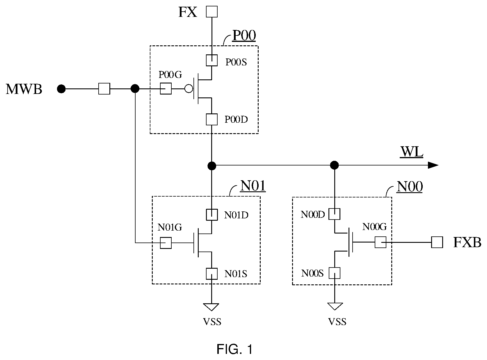
Referring to , is a schematic diagram of a circuit of a word line driver. The word line driver includes: a first PMOS transistor P 00 , a first NMOS transistor N 00 , and a second NMOS transistor N 01 , the first PMOS transistor P 00 being provided with a gate P 00 G connected to a gate N 01 G of the second NMOS transistor N 01 and configured to receive a first control signal MWB, a source P 00 S configured to receive a second control signal FX, and a drain P 00 D connected to a drain N 01 D of the second NMOS transistor N 01 , the first NMOS transistor N 00 being provided with a gate N 00 G configured to receive a second control complementary signal FXB, a drain N 00 D of the first NMOS transistor N 00 and the drain N 01 D of the second NMOS transistor N 01 being configured to be connected to a word line WL, and a source N 00 S of the first NMOS transistor N 00 and a source N 01 S of the second NMOS transistor N 01 being connected to a low level VSS. Referring to , is a schematic diagram of a layout of a word line driver. The first PMOS transistor P 00 and the second NMOS transistor N 01 are arranged side by side in a first extension direction D 1 , the second NMOS transistor N 01 and the first NMOS transistor N 00 are arranged side by side in a second extension direction D 2 , and the first extension direction D 1 is perpendicular to the second extension direction D 2 .
With the miniaturization of the word line driver, the channel length of the first NMOS transistor N 00 and the channel length of the second NMOS transistor N 01 are gradually shortened, which will affect the reliability of the NMOS transistors. However, since the second NMOS transistor N 01 and the first NMOS transistor N 00 are arranged side by side in the second extension direction D 2 , and the channel direction of the first NMOS transistor N 00 and the channel direction of the second NMOS transistor N 01 are both the second extension direction D 2 , the channel length of single NMOS transistor is limited. Therefore, the corresponding performance cannot be improved by extending the channel length of the first NMOS transistor N 00 and the channel length of the second NMOS transistor N 01 .
Referring to , is a schematic diagram of a layout of a word line driver array. The word line driver array includes a second PMOS transistor P 00 , a fourth PMOS transistor P 10 , a third NMOS transistor N 00 , a fourth NMOS transistor N 01 , a fifth NMOS transistor N 10 , and an sixth NMOS transistor N 11 , where, a drain N 00 D of the third NMOS transistor N 00 and a drain N 10 D of the fifth NMOS transistor N 10 are arranged side by side in the first extension direction D 1 , the drain N 00 D of the third NMOS transistor N 00 and a drain N 01 D of the fourth NMOS transistor N 01 share a same metal contact marked as a first metal contact, and the drain N 10 D of the fifth NMOS transistor N 10 and a drain N 11 D of the sixth NMOS transistor N 11 share a same metal contact marked as a second metal contact.
There are two NMOS transistors arranged side by side in the second extension direction D 2 . Therefore, the size of single NMOS transistor is limited, and the spacing between gates of different NMOS transistors is narrow. The first metal contact and the second metal contact are located between the adjacent gates in the second extension direction D 2 . Therefore, the range of optional positions of the first metal contact and the second metal contact in the second extension direction D 2 is limited by the spacing between the adjacent gates. Moreover, the spacing between the gates is narrow. Therefore, the spacing between the first metal contact and the second metal contact in the second extension direction D 2 is narrow. When the first metal contact and the second metal contact are controlled to be in contact with and connect the corresponding word lines, the word lines are provided with the first extension direction D 1 , and the spacing between the first metal contact and the second metal contact in the second extension direction D 2 is narrow. Therefore, electric isolation between the adjacent word lines can be ensured by bending the word lines. The bending of the word lines is not beneficial to improve the layout regularity of the semiconductor device, or even possibly affects the electric performance of the word lines.
Referring to to , and are schematic diagrams of a layout of a word line driver array, is a schematic diagram of a circuit of a word line driver array, and differs from in that additionally shows the word lines. A first word line WL<n> is configured to connect a drain Px 00 D of a second PMOS transistor Px 00 , a drain Nx 00 D of a third NMOS transistor Nx 00 , and a drain Nx 01 D of a fourth NMOS transistor Nx 01 in the first word line driver. A second word line WL<n+2> is configured to connect a drain Px 10 D of a third PMOS transistor Px 10 , a drain Nx 10 D of a fifth NMOS transistor Nx 10 , and a drain Nx 11 D of a sixth NMOStransistor Nx 11 in the second word line driver. A third word line WL<n+4> is configured to connect a drain Px 20 D of a fourth PMOS transistor Px 20 , a drain Nx 20 D of a seventh PMOS transistor Nx 20 , and a drain Nx 21 D of a eighth NMOS transistor Nx 21 in the third word line driver. A fourth word line WL<n+6> is configured to connect a drain Px 30 D of a fifth PMOS transistor Px 30 , a drain Nx 30 D of a ninth NMOS transistor Nx 30 , and a drain Nx 31 D of a tenth NMOS transistor Nx 31 in the fourth word line driver.
In addition, each word line driver is configured to receive the corresponding second control signal FX and second control complementary signal FXB. shows a plurality of second control signals FX, namely FX 0 , FX 1 , FX 2 , and FX 3 , and shows a plurality of second control complementary signals FXB, namely FXB 0 , FXB 1 , FXB 2 , and FXB 3 .
It can be known from that the drain Nx 30 D of the x30-th NMOS transistor Nx 30 and the drain Nx 31 D of the tenth NMOS transistor Nx 31 are connected and share a same metal contact marked as a third metal contact, and the drain Nx 20 D of the seventh NMOStransistor Nx 20 and the drain Nx 21 D of the eighth NMOS transistor Nx 21 are connected and share a same metal contact marked as a fourth metal contact. When the third metal contact is connected to the fourth word line WL<n+6>, and the fourth metal contact is connected to the third word line WL<n+4>, it is impossible to respectively connect the third metal contact and the fourth metal contact with different straight and parallel word lines, and it is necessary to additionally bend the third word line WL<n+4> and the fourth word line WL<n+6>. In addition, taking the third metal contact as an example, since the optional position range of the third metal contact in the second extension direction D 2 is narrow, the spacing between the third metal contact and a metal contact of the drain of the corresponding PMOS transistor in the second extension direction D 2 may be large, and a same word line also needs to be bent when being connected to a different metal contact, which is not beneficial to promote the layout regularity of the semiconductor device and improve the electric performance of the word line.
To make the objectives, technical solutions and advantages of the embodiments of the present disclosure clearer, the embodiments of the present disclosure are described below with reference to the accompanying drawings.
It should be noted that, each MOS transistor is provided with a corresponding gate, source and drain. For the clarity of the illustration and the brevity of the description, each gate, source and drain are identified in the illustration herein. However, each gate, source and drain are not specifically described in the description, but reference numerals are publicly described by explaining naming rules of the reference numerals. The naming rules are applicable to the whole text, that is to say, all the reference numerals that may be applicable to explanation rules are deemed to have been described in the description.
Taking Px 00 G as an example, the first bit from right to left indicates the polarity of the transistor, G indicates the gate, S indicates the source, and D indicates the drain. The second bit indicates the number of the same type of transistor in each word line driver. Herein, each word line driver includes one PMOS transistor and two NMOS transistors. Therefore, the value of this bit is 0 or 1, 0 indicates the first NMOS transistor or the first PMOS transistor, and 1 indicates the second NMOS transistor. The third bit indicates the number of word line driver in the word line driver array. The word line driver array includes a plurality of word line drivers, 0 indicates the first word line driver, 1 indicates the second word line driver, and 2 indicates the third word line driver, and 3 indicates the fourth word line driver. The fourth bit indicates the number of word line driver array in the semiconductor structure, and the semiconductor structure includes a plurality of word line driver arrays. If there are a plurality of arrays in the illustration, x may be set to different natural numbers (starting from 0) to identify different arrays. If there is only one array in the illustration, the fourth bit may be set to 0 or omitted directly. The last bit indicates the type of the transistor; if it is “P”, it is a PMOS transistor; and if it is “N”, it is an NMOS transistor.
Referring to and , the word line driver includes: a first PMOS transistor P 00 , a first NMOS transistor N 00 , and a second NMOS transistor N 01 , the first PMOS transistor P 00 being provided with a gate P 00 G connected to a gate N 01 G of the second NMOS transistor N 01 and configured to receive a first control signal MWB, a source P 00 S configured to receive a second control signal FX, and a drain P 00 D connected to a drain N 01 D of the second NMOS transistor N 01 , the first NMOS transistor N 00 being provided with a gate N 00 G configured to receive a second control complementary signal FXB, and a drain N 00 D of the first NMOS transistor N 00 and the drain N 01 D of the second NMOS transistor N 01 being configured to be connected to a word line WL. The word line WL is provided with a first extension direction D 1 , and the first PMOS transistor P 00 , the first NMOS transistor N 00 , and the second NMOS transistor N 01 are arranged side by side in the first extension direction D 1 .
The first NMOS transistor N 00 and the second NMOS transistor N 01 are arranged side by side in the first extension direction D 1 . Therefore, in a second extension direction D 2 perpendicular to the first extension direction D 1 , there is only one NMOS transistor arranged independently, thus facilitating enlarging the size range of the first NMOS transistor N 00 and the second NMOS transistor N 01 in the second extension direction D 2 . Under overall miniaturization of the word line driver, if the channel direction of the first NMOS transistor N 00 and the channel direction of the second NMOS transistor N 01 are the second extension direction D 2 , the reliability of the NMOS transistors may be promoted by extending the channel length of the first NMOS transistor N 00 and the channel length of the second NMOS transistor N 01 .
In some embodiments, the channel of the first PMOS transistor P 00 and the channel of the second NMOS transistor N 01 are provided with the second extension direction D 2 . In this way, it is beneficial to extend the channel length of the first PMOS transistor P 00 and the channel length of the second NMOS transistor N 01 , and promote the electric performance of the first PMOS transistor P 00 and the electric performance of the second NMOS transistor N 01 .
In some embodiments, the channel of the first NMOS transistor N 00 is provided with the first extension direction D 1 . In this way, the gate N 00 G and the drain N 00 D of the first NMOS transistor N 00 are provided with the second extension direction D 2 . By extending the length of the drain N 00 D of the first NMOS transistor N 00 in the second extension direction D 2 , the optional position range of the metal contact of the drain N 00 D in the second extension direction D 2 may be enlarged, and the vertical spacing between the drain N 00 D of the first NMOS transistor N 00 and the drain N 01 D of the second NMOS transistor N 01 in the second extension direction D 2 may be reduced, thereby reducing the bending degree of the word line connected to the drain N 00 D of the first NMOS transistor N 00 and the drain N 01 D of the second NMOS transistor N 01 , and promoting the regularity of the word line.
In some embodiments, the first PMOS transistor P 00 is located between the first NMOS transistor N 00 and the second NMOS transistor N 01 . In some other embodiments, the second NMOS transistor N 01 is located between the first NMOS transistor N 00 and the first PMOS transistor P 00 . That is to say, the first NMOS transistor N 00 whose channel is provided with the first extension direction D 1 cannot be located at the middle position, or should be located at the edge position. In this way, since the width of the first NMOS transistor N 00 in the second extension direction D 2 is large, when the word line is not bent, a word line connecting point located outside the word line driver has a large optional position range, thereby facilitating promoting the regularity of the word line.
In some embodiments, one side edge of the drain N 00 D of the first NMOS transistor N 00 is flush with one side edge of the drain N 01 D of the second NMOS transistor N 01 distant from the gate N 01 G. In this way, the word line connected to the drain P 00 D of the first PMOS transistor P 00 and the drain N 01 D of the second NMOS transistor N 01 is connected to the drain N 00 D of the first NMOS transistor N 00 when being not bent or less bent, thereby promoting the regularity of the word line and the electric performance of the word line.
In some embodiments, in the second extension direction D 2 , the width of the drain N 00 D of the first NMOS transistor N 00 is equal to the sum of a width of the gate N 01 G of the second NMOS transistor N 01 and a width of the drain N 01 D of the second NMOS transistor N 01 , and the other side edge of the drain N 00 D of the first NMOS transistor N 00 is flush with one side edge of the gate N 01 G of the second NMOS transistor N 01 distant from the drain N 01 D.
In this embodiment, the first PMOS transistor P 00 , the first NMOS transistor N 00 , and the second NMOS transistor N 01 are arranged side by side, thereby facilitating enlarging the channel length range of the first NMOS transistor N 00 and the second NMOS transistor N 01 . Thus, under gradual miniaturization of the word line driver, it is ensured that the first NMOS transistor N 00 and the second NMOS transistor N 01 each have a large channel length, thereby ensuring that the first NMOS transistor N 00 and the second NMOS transistor N 01 have higher reliability.
The embodiments of the present disclosure also provide a word line driver array. Referring to , the word line driver array includes: at least two of the word line drivers as described above marked as a first word line driver and a second word line driver. The first word line driver includes a second PMOS transistor P 00 , a third NMOS transistor N 00 , and a fourth NMOS transistor N 01 . The second word line driver includes a fourth PMOS transistor P 10 , a fifth NMOS transistor N 10 , and an sixth NMOS transistor N 11 . The first word line driver and the second word line driver are arranged side by side in a first extension direction D 1 . A gate P 00 G of the second PMOS transistor P 00 is connected to a gate P 10 G of the fourth PMOS transistor P 10 and located on a first straight line parallel to the first extension direction D 1 , a gate N 01 G of the fourth NMOS transistor N 01 is connected to a gate N 11 G of the sixth NMOS transistor N 11 and located on the first straight line, and a gate N 00 G of the third NMOS transistor N 00 and a gate N 10 G of the fifth NMOS transistor N 10 are arranged in parallel.
In some embodiments, the source N 00 S of the third NMOS transistor N 00 is connected to the source N 10 S of the fifth NMOS transistor N 10 , and the source of the fourth NMOS transistor N 01 is connected to the source of the sixth NMOS transistor N 11 . In some other embodiments, the gate of the fourth PMOS transistor P 10 is connected to the gate of the fourth NMOS transistor N 01 . In the first extension direction D 1 , the projection of the gate of the second PMOS transistor P 00 , the projection of the gate of the fourth PMOS transistor P 10 , the projection of the gate of the fourth NMOS transistor N 01 , and the projection of the gate of the sixth NMOS transistor N 11 overlap. That is to say, the gates do not need to be bent in the first extension direction D 1 .
In some embodiments, the channel of the third NMOS transistor N 00 and the channel of the fifth NMOS transistor N 10 are provided with the first extension direction D 1 . In the first extension direction D 1 , the orthographic projection of the drain N 00 D of the third NMOS transistor N 00 overlaps with the orthographic projection of the drain N 10 D of the fifth NMOS transistor N 10 . Furthermore, one side edge of the drain N 00 D of the third NMOS transistor N 00 , one side edge of the drain N 10 D of the fifth NMOS transistor N 10 , one side edge of the drain N 01 D of the fourth NMOS transistor N 01 , and one side edge of the drain N 11 D of the sixth NMOS transistor N 11 are located on a same straight line. Correspondingly, the other side of the drain N 00 D of the third NMOS transistor N 00 , the other side of the drain N 10 D of the fifth NMOS transistor N 10 , the side edge of the gate of the fourth NMOS transistor N 01 distant from the drain N 01 D, and the side edge of the gate of the sixth NMOS transistor N 11 distant from the drain N 11 D are located on a same straight line.
In some embodiments, referring to to , and are schematic diagrams of a layout of a word line driver array according to an embodiment of the present disclosure, and is a schematic diagram of a circuit structure in a layout shown in . differs from in that shows the word line. The word line driver array further includes: a third word line driver including a fourth PMOS transistor Px 20 , a seventh NMOS transistor Nx 20 , and a eighth NMOS transistor Nx 21 ; and a fourth word line driver including a fifth PMOS transistor Px 30 , a ninth NMOS transistor Nx 30 , and a tenth NMOS transistor Nx 31 . In the first extension direction, the third NMOS transistor Nx 00 , the fifth NMOS transistor Nx 10 , the tenth NMOS transistor Nx 31 , the eighth NMOS transistor Nx 21 , the fourth PMOS transistor Px 20 , the fifth PMOS transistor Px 30 , the second PMOS transistor Px 00 , the fourth PMOS transistor Px 10 , the sixth NMOS transistor Nx 11 , the fourth NMOS transistor Nx 01 , the seventh NMOS transistor Nx 20 , and the ninth NMOS transistor Nx 30 are arranged side by side.
In addition, each word line driver is configured to receive the corresponding second control signal FX and second control complementary signal FXB. includes a plurality of second control signals FX, namely FX 0 , FX 2 , FX 4 , and FX 6 , and includes a plurality of second control complementary signals FXB, namely FXB 0 , FXB 2 , FXB 4 , and FXB 6 .
In some embodiments, the channel of the seventh NMOS transistor Nx 20 and the channel of the ninth NMOS transistor Nx 30 are provided with the first extension direction D 1 , and in the first extension direction D 1 , the orthographic projection of the drain Nx 00 D of the third NMOS transistor Nx 00 , the orthographic projection of the drain Nx 10 D of the fifth NMOS transistor Nx 10 , the orthographic projection of the drain Nx 20 D of the seventh NMOS transistor Nx 20 , and the orthographic projection of the drain Nx 30 D of the ninth NMOS transistor Nx 30 overlap.
In some embodiments, referring to , in the first extension direction D 1 , the third NMOS transistor Nx 00 , the fifth NMOS transistor Nx 10 , the tenth NMOS transistor Nx 31 , the eighth NMOS transistor Nx 21 , the fourth PMOS transistor Px 20 , the fifth PMOS transistor Px 30 , the second PMOS transistor Px 00 , the fourth PMOS transistor Px 10 , the sixth NMOS transistor Nx 11 , the fourth NMOS transistor Nx 01 , the seventh NMOS transistor Nx 20 , and the ninth NMOS transistor Nx 30 are arranged in sequence. Moreover, a plurality of word line drivers having the same arrangement are arranged side by side in the second extension direction D 2 to constitute the semiconductor structure.
In some embodiments, referring to , in the first extension direction D 1 , the sixth NMOS transistor Nx 11 , the fourth NMOS transistor Nx 01 , the tenth NMOS transistor Nx 31 , the eighth NMOS transistor Nx 21 , the fourth PMOS transistor Px 20 , the fifth PMOS transistor Px 30 , the second PMOS transistor Px 00 , the fourth PMOS transistor Px 10 , the third NMOS transistor Nx 00 , the fifth NMOS transistor Nx 10 , the seventh NMOS transistor Nx 20 , and the ninth NMOS transistor Nx 30 are arranged in sequence. Moreover, a plurality of word line drivers having the same arrangement are arranged side by side in the second extension direction D 2 to constitute the semiconductor structure.
In some embodiments, referring to , in the first extension direction D 1 , the third NMOS transistor Nx 00 , the fifth NMOS transistor Nx 10 , the second PMOS transistor Px 00 , the fourth PMOS transistor Px 10 , the sixth NMOS transistor Nx 11 , the fourth NMOS transistor Nx 01 , the tenth NMOS transistor Nx 31 , the eighth NMOS transistor Nx 21 , the fourth PMOS transistor Px 20 , the fifth PMOS transistor Px 30 , the seventh NMOS transistor Nx 20 , and the ninth NMOS transistor Nx 30 are arranged in sequence. Moreover, a plurality of word line drivers having the same arrangement are arranged side by side in the second extension direction D 2 to constitute the semiconductor structure.
In some embodiments, referring to , in the first extension direction D 1 , the third NMOS transistor Nx 00 , the fifth NMOS transistor Nx 10 , the seventh NMOS transistor Nx 20 , the ninth NMOS transistor Nx 30 , the sixth NMOS transistor Nx 11 , the fourth NMOS transistor Nx 01 , the tenth NMOS transistor Nx 31 , the eighth NMOS transistor Nx 21 , the fourth PMOS transistor Px 20 , the fifth PMOS transistor Px 30 , the second PMOS transistor Px 00 , and the fourth PMOS transistor Px 10 are arranged in sequence. Moreover, a plurality of word line drivers having the same arrangement are arranged side by side in the second extension direction D 2 to constitute the semiconductor structure.
In some embodiments, referring to , in the first extension direction D 1 , the third NMOS transistor Nx 00 , the fifth NMOS transistor Nx 10 , the sixth NMOS transistor Nx 11 , the fourth NMOS transistor Nx 01 , the tenth NMOS transistor Nx 31 , the eighth NMOS transistor Nx 21 , the fourth PMOS transistor Px 20 , the fifth PMOS transistor Px 30 , the second PMOS transistor Px 00 , the fourth PMOS transistor Px 10 , the seventh NMOS transistor Nx 20 , and the ninth NMOS transistor Nx 30 are arranged in sequence. Moreover, a plurality of word line drivers having the same arrangement are arranged side by side in the second extension direction D 2 to constitute the semiconductor structure.
The present disclosure provides a new word line driver array. By adjusting the side-by-side arrangement direction and channel direction of the NMOS transistors, the electric performance and layout regularity of the word line driver array are promoted.
The embodiments of the present disclosure also provide a semiconductor structure. Referring to and , shows the word line on the basis of . The semiconductor structure includes: at least two of the word line driver arrays as described above marked as a first word line driver array and a second word line driver array. The first word line driver array and the second word line driver array are arranged side by side in a second extension direction D 2 . The first word line driver array includes a eleventh NMOS transistor N 000 , a twelfth NMOS transistor N 010 , a thirteenth NMOS transistor N 020 , and a fourteenth NMOS transistor N 030 . The second word line driver array includes a fifteenth NMOS transistor N 100 , a sixteenth NMOS transistor N 110 , a seventeenth NMOS transistor N 120 , and a eighteenth NMOS transistor N 130 . A gate of the eleventh NMOS transistor N 000 is connected to a gate of the fifteenth NMOS transistor N 100 and located on a first straight line; a gate of the twelfth NMOS transistor N 010 is connected to a gate of the sixteenth NMOS transistor N 110 and located on a second straight line; a gate of the thirteenth NMOS transistor N 020 is connected to a gate of the seventeenth NMOS transistor N 120 and located on a third straight line; a gate of the fourteenth NMOS transistor N 030 is connected to a gate of the eighteenth NMOS transistor N 130 and located on a fourth straight line; and the first straight line, the second straight line, the third straight line, and the fourth straight line are provided with the second extension direction and parallel to each other.
The embodiments or implementations of this specification are described in a progressive manner, and each embodiment focuses on differences from other embodiments. The same or similar parts between the embodiments may refer to each other.
In the description of this specification, the description with reference to terms such as “an embodiment”, “an exemplary embodiment”, “some implementations”, “a schematic implementation”, and “an example” means that the specific feature, structure, material, or characteristic described in combination with the implementation(s) or example(s) is included in at least one implementation or example of the present disclosure.
In this specification, the schematic expression of the above terms does not necessarily refer to the same implementation or example. Moreover, the described specific feature, structure, material or characteristic may be combined in an appropriate manner in any one or more implementations or examples.
It should be noted that in the description of the present disclosure, the terms such as “center”, “top”, “bottom”, “left”, “right”, “vertical”, “horizontal”, “inner” and “outer” indicate the orientation or position relationships based on the accompanying drawings. These terms are merely intended to facilitate description of the present disclosure and simplify the description, rather than to indicate or imply that the mentioned apparatus or element must have a specific orientation and must be constructed and operated in a specific orientation. Therefore, these terms should not be construed as a limitation to the present disclosure.
It can be understood that the terms such as “first” and “second” used in the present disclosure can be used to describe various structures, but these structures are not limited by these terms. Instead, these terms are merely intended to distinguish one structure from another.
The same elements in one or more accompanying drawings are denoted by similar reference numerals. For the sake of clarity, various parts in the accompanying drawings are not drawn to scale. In addition, some well-known parts may not be shown. For the sake of brevity, a structure obtained by implementing a plurality of steps may be shown in one figure. In order to understand the present disclosure more clearly, many specific details of the present disclosure, such as the structure, material, size, processing process, and technology of the device, are described below. However, as those skilled in the art can understand, the present disclosure may not be implemented according to these specific details.
Finally, it should be noted that the above embodiments are merely intended to explain the technical solutions of the present disclosure, rather than to limit the present disclosure. Although the present disclosure is described in detail with reference to the above embodiments, those skilled in the art should understand that they may still modify the technical solutions described in the above embodiments, or make equivalent substitutions of some or all of the technical features recorded therein, without deviating the essence of the corresponding technical solutions from the scope of the technical solutions of the embodiments of the present disclosure.
INDUSTRIAL APPLICABILITY
In the word line driver, the word line driver array, and the semiconductor structure provided in the embodiments of the present disclosure, the zero PMOS transistor, the zero NMOS transistor, and the second NMOS transistor are arranged side by side in the first extension direction, the extension range of the first NMOS transistor and the extension range of the second NMOS transistor perpendicular to the first extension direction are enlarged, and under overall miniaturization of the word line driver, if the channel direction of the first NMOS transistor and the channel direction of the second NMOS transistor are perpendicular to the first extension direction, the channel length of the first NMOS transistor and the channel length of the second NMOS transistor may be extended, thereby improving the reliability of the NMOS transistors.
Figures (18)
Citations
This patent cites (8)
- US6192000
- US7599232
- US9318175
- US2012/0320699
- US2019/0189186
- US101110263
- US105719684
- US109935258