Abstract
A semiconductor device includes a protection element configured by a MOSFET, and the protection element has a multilayer metal wiring structure. The multilayer metal wiring structure includes drain connection wirings connected to drain regions of the MOSFET and source connection wirings connected to source regions of the MOSFET. In a part of a layer of the multilayer metal wiring structure where both the drain connection wirings and the source connection wirings are present, only either the drain connection wirings or the source connection wirings are laid out in a grained pattern.
Claims (5)
1. A semiconductor device comprising a protection element configured by a MOSFET, wherein the protection element has a multilayer metal wiring structure, wherein the multilayer metal wiring structure includes drain connection wirings connected to drain regions of the MOSFET and source connection wirings connected to source regions of the MOSFET, and wherein, in a part of a layer of the multilayer metal wiring structure where both the drain connection wirings and the source connection wirings are present, only either the drain connection wirings or the source connection wirings are laid out in a grained pattern.
4. A semiconductor device comprising a protection element configured by a diode, wherein the protection element has a multilayer metal wiring structure, wherein the multilayer metal wiring structure includes anode connection wirings connected to anode regions of the diode and cathode connection wirings connected to cathode regions of the diode, and wherein, in a part of a layer of the multilayer metal wiring structure where both the anode connection wirings and the cathode connection wirings are present, only either the anode connection wirings or the cathode connection wirings are laid out in a grained pattern.
5. A semiconductor device comprising a protection element configured by a thyristor, wherein the protection element has a multilayer metal wiring structure, wherein the multilayer metal wiring structure includes anode connection wirings connected to anode regions of the thyristor and cathode connection wirings connected to cathode regions of the thyristor, and wherein, in a part of a layer of the multilayer metal wiring structure where both the anode connection wirings and the cathode connection wirings are present, only either the anode connection wirings or the cathode connection wirings are laid out in a grained pattern.
Show 2 dependent claims
2. The semiconductor device according to claim 1 , wherein both the drain connection wirings and the source connection wirings are laid out in a grained pattern, and wherein the drain connection wirings laid out in the grained pattern and the source connection wirings laid out in the grained pattern are formed in different layers in the multilayer metal wiring structure.
3. The semiconductor device according to claim 2 , wherein the drain connection wirings laid out in the grained pattern and the source connection wirings laid out in the grained pattern are arranged alternately diagonally in a plan view.
Full Description
Show full text →
CROSS-REFERENCE TO RELATED APPLICATIONS
The disclosure of Japanese Patent Application No. 2021-153671 filed on Sep. 21, 2021 including the specification, drawings and abstract is incorporated herein by reference in its entirety.
BACKGROUND
The present disclosure relates to a semiconductor device, and is a technique effectively applied to a semiconductor device having a protection element (protection circuit) against a surge pulse.
Some semiconductor devices have a protection element against a surge pulse. As a proposal of this kind of semiconductor devices, for example, Japanese Unexamined Patent Application Publication No. 2020-161721 is available.
There are disclosed techniques listed below. [Patent Document 1] Japanese Unexamined Patent Application Publication No. 2020-161721
SUMMARY
In the semiconductor device mounted in an automotive electronic control unit (ECU), tests are executed with a surge pulse width having a longer time axis than the ESD (Electro-Static Discharge (surge)) pulse. Even for consumer semiconductor devices, it has been gradually required to strengthen the long pulse resistance.
An object of the present disclosure is to provide a technique capable of improving the discharge performance or heat dissipation performance of a protection element (protection circuit) against a surge having a long pulse width.
Other problems and novel features will be apparent from the description of this specification and accompanying drawings.
The outline of the representative embodiment of the present disclosure will be briefly described as follows.
A semiconductor device according to the embodiment includes a protection element configured by a MOSFET, and the protection element has a multilayer metal wiring structure. The multilayer metal wiring structure includes drain connection wirings connected to drain regions of the MOSFET and source connection wirings connected to source regions of the MOSFET. In a part of a layer of the multilayer metal wiring structure where both the drain connection wirings and the source connection wirings are present, only either the drain connection wirings or the source connection wirings are laid out in a grained pattern.
By the semiconductor device according to the embodiment described above, it is possible to improve the discharge performance or heat dissipation performance of a protection circuit against a surge having a long pulse width.
BRIEF DESCRIPTION OF THE DRAWINGS
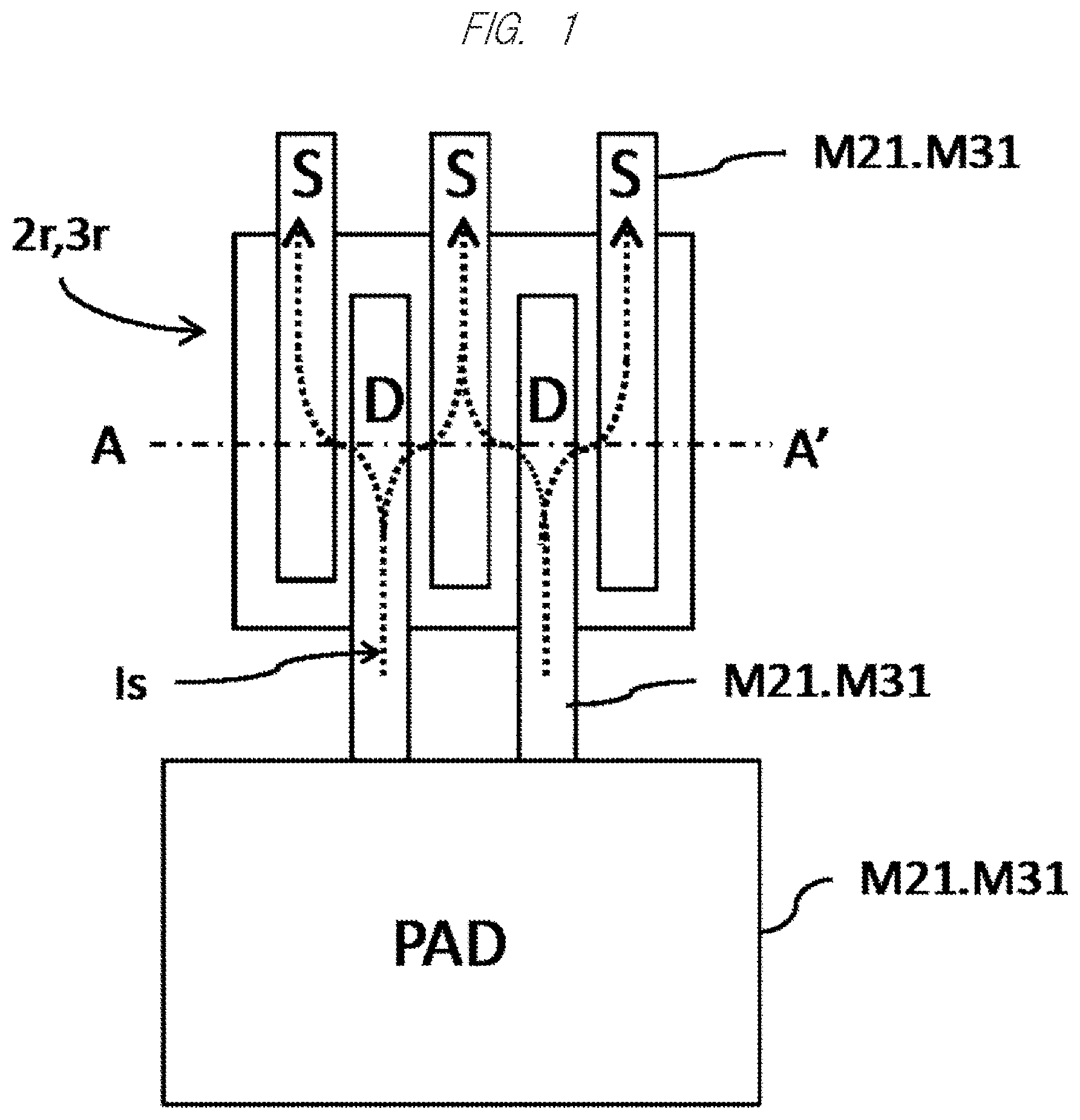
is an explanatory plan view of a layout of a protection circuit according to the comparative example.
is a cross-sectional view of the protection circuit taken along the line A-A′ in .
is an explanatory plan view of a layout of a protection circuit according to the first example.
is a cross-sectional view of the protection circuit taken along the line A-A′ in .
is a cross-sectional view of the protection circuit taken along the line B-B′ in .
is an explanatory plan view of a layout of a protection circuit according to the second example.
is a cross-sectional view of the protection circuit taken along the line A-A′ in .
is a cross-sectional view of the protection circuit taken along the line B-B′ in .
is an explanatory plan view of an arrangement example in a second wiring layer M 2 in a layout of a protection circuit according to the third example.
is an explanatory plan view of an arrangement example in a third wiring layer M 3 in the layout of the protection circuit according to the third example.
is a cross-sectional view of the protection circuit taken along the line A-A′ in .
is a cross-sectional view of the protection circuit taken along the line B-B′ in .
is a graph showing a measurement result of the breakdown power of protection elements having different silicon areas in the case where the surge pulse width is in the range of the surge test for the consumer semiconductor devices.
is a graph showing a measurement result of the breakdown power of protection elements having different silicon areas in the case where the surge pulse width is in the range of the surge test for the automotive semiconductor devices.
DETAILED DESCRIPTION
Hereinafter, the comparative example, the embodiment, and the examples will be described with reference to drawings. However, in the following description, the same components are denoted by the same reference characters and the repetitive description thereof will be omitted in some cases. Note that the drawings may be shown schematically as compared with an actual aspect in order to make the description clearer, but they are mere examples and do not limit the interpretation of the present invention.
Before the description of the embodiment, a configuration example of a layout of a protection circuit according to the comparative example will be described with reference to and . is an explanatory plan view of the layout of the protection circuit according to the comparative example. is a cross-sectional view of the protection circuit taken along the line A-A′ in . illustrates wirings M 21 composed of a second wiring layer M 2 and wirings M 31 composed of a third wiring layer M 3 in the wiring layout of the protection circuit.
As shown in and , a MOS protection element 3 r constituting a protection circuit 2 r has gate electrodes G, source regions S, and drain regions D. The source regions S and the drain regions D are formed in a silicon semiconductor substrate (SiSub) 1 r , and the gate electrodes G are formed on an upper side of a gate oxide film (not shown) formed on the surface of the semiconductor substrate 1 r.
The source region S is electrically connected to a fourth wiring M 41 composed of a fourth wiring layer M 4 through a first via electrode V 1 , a first wiring M 11 composed of a first wiring layer M 1 , a second via electrode V 2 , a second wiring M 21 composed of a second wiring layer M 2 , a third via electrode V 3 , a third wiring M 31 composed of a third wiring layer M 3 , and a fourth via electrode V 4 . The fourth wiring M 41 can be paraphrased as a bus wiring.
The drain region D is electrically connected to the third wiring M 31 through the first via electrode V 1 , the first wiring M 11 , the second via electrode V 2 , the second wiring M 21 , and the third via electrode V 3 . The second wiring M 21 and the third wiring M 31 to which the drain region D is connected are connected to a pad electrode PAD. The first via electrode V 1 can be paraphrased as a contact electrode.
The first to fourth wirings M 11 to M 41 and the first to fourth via electrodes V 1 to V 4 are made of metal such as copper (Cu) or aluminum (Al). The first to fourth wirings M 11 to M 41 and the first to fourth via electrodes V 1 to V 4 are covered with an insulating film (for example, silicon oxide film (SiO 2 )) 4 r having a relatively low thermal conductivity.
As shown in , when a surge pulse is applied to the pad electrode PAD, a surge current Is indicated by the dotted arrow flows. When the MOS protection element 3 r is an N-type MOSFET (Metal-Oxide-Semiconductor Field Effect Transistor), the fourth wiring M 41 is a ground potential (first reference potential) GND. On the other hand, when the MOS protection element 3 r is a P-type MOSFET, the fourth wiring M 41 is a power supply potential (second reference potential) VDD (VDD>GND).
and are graphs each showing a measurement result of the breakdown power of protection elements (N-type MOSFETs) having different silicon areas. shows the measurement result in the case where the surge pulse width is in the range of the surge test for the consumer semiconductor devices. shows the measurement result in the case where the surge pulse width is in the range of the surge test for the automotive semiconductor devices. In and , the vertical axis represents the breakdown power Pf(W) per unit Si area, and the horizontal axis represents the pulse width (sec) of the surge pulse. Regarding the Si area, 5V-NA is small (×1), 5V-NB is medium (×2), and 5V-NC is large (×3). Also, the number of metal wirings on the side of the drain (D) is 28 for 5V-NA, 44 for 5V-NB, and 56 for 5V-NC. Here, as the surge test for automotive semiconductor devices (also referred to as the ECU surge test), for example, the test with test voltage: −150 V, pulse width: 2 ms, and energy: 250 mJ or the test with test voltage: +112 V, pulse width: 50 μs, and energy: 20 mJ is available. As the surge test for consumer semiconductor devices, the test with test voltage: +/−2 kV, pulse width: 150 ns, and energy: 800 nJ is available.
As shown in , in the time region TESD of the surge pulse in the ESD (Electro-Static Discharge (surge)) test for consumer semiconductor devices, the protection performance per unit Si area is almost the same in 5V-NA, 5V-NB, and 5V-NC.
On the other hand, as shown in , in the time region TECU of the surge pulse in the ECU surge test, a difference in protection performance due to the number of metal wirings on the side of the drain appears when the pulse width of the surge pulse becomes 20 μs or more. Namely, it can be found that, when the pulse width is 20 μs or more, the performance with respect to the breakdown power Pf is lowered as the number of metal wirings on the side of the drain (D) becomes larger, and the value of the breakdown power Pf has the relationship of 5V-NA>5V-NB>5V-NC.
In summary, it can be said as follows.
(1) With the miniaturization of semiconductor elements formed in semiconductor devices and the increase in the number of metal wiring layers, the performance of the protection element deteriorates significantly due to the influence of heat generation of the metal wiring caused by the surge having a long pulse width.
(2) In the narrow pitch metal wiring region, the metal wiring layers (M 11 to M 41 , V 1 to V 4 ) are covered with the interlayer insulating film 4 r having a low thermal conductivity made of a silicon oxide film (SiO 2 ) or the like, so that heat is accumulated between the adjacent wirings, which is the main cause of the performance deterioration of the protection element. Note that the thermal conductivity of copper (Cu) is 403 (W/m·K), and the thermal conductivity of aluminum (Al) is 236 (W/m·K). On the other hand, the thermal conductivity of silicon (Si) is 160 (W/m·K), and the thermal conductivity of the silicon oxide film (SiO 2 ) is 1.3 (W/m·K).
(3) It is possible to reduce the influence of the heat accumulated between the metal wirings (M 11 to M 41 or the like) by expanding the wiring pitch (space between wirings). In this case, however, there is a problem that the Si area of the protection element increases and the chip cost of the semiconductor device increases.
EMBODIMENT
In order to solve the problems described above, a protection element 3 according to the embodiment of the present disclosure has the following configuration.
In the protection element 3 formed on one main surface of a semiconductor substrate (SiSub),
•
• in order to improve the surge resistance against the long surge pulse width (for example, several tens μs or more), • in the shape of the metal wirings (M 1 d to M 4 d , M 1 s to M 3 s ) connected to the protection element 3 (here, the case where the protection element 3 is a MOSFET is described), • in the layer in which the multilayer first connection wirings (referred to also as, for example, drain connection wirings) connected between the pad electrodes PAD and the drain regions D of the protection element 3 and the multilayer second connection wirings (referred to also as, for example, source connection wirings) connected between the source regions S of the protection element 3 and the bus wiring (M 41 ) to which the ground potential GND or the power supply potential VDD is supplied are arranged adjacent to each other, • either the connection wirings to the pad electrodes PAD (first connection wirings) or the connection wirings to the bus wiring 41 (second connection wirings) are laid out in a grained pattern.
By the layout arrangement described above, the density of the metal wiring can be reduced without increasing the Si area of the protection element 3 . Since the density of the metal wiring can be reduced, it is possible to avoid the adverse effect of the heat accumulated in the interlayer insulating film due to the heat generation in the metal wiring region. As a result, it is possible to improve the discharge performance or heat dissipation performance of the protection element 3 against the surge having a long pulse width. For example, in a surge test with a pulse width of 50 μs, the surge resistance per unit Si area can be improved by 1.5 to 2.0 times as compared with the comparative example (see and ).
When the protection element 3 is a protection element configured by a diode or a thyristor (SCR: Silicon Controlled Rectifier), the drain connection wiring and the source connection wiring can be paraphrased as an anode connection wiring and a cathode connection wiring. The anode connection wiring is connected to the anode region of the diode or thyristor, and the cathode connection wiring is connected to the cathode region of the diode or thyristor.
Hereinafter, each example will be described with reference to the drawings.
First Example
Next, a configuration example of a layout of a protection circuit 2 according to the first example will be described with reference to to . is an explanatory plan view of a layout of a protection circuit according to the first example. is a cross-sectional view of the protection circuit taken along the line A-A′ in . is a cross-sectional view of the protection circuit taken along the line B-B′ in . In , in the wiring layout of the protection circuit, the wirings M 2 s , M 2 d , and M 2 p composed of the second wiring layer M 2 are illustrated.
In the first example, in the metal wiring structure of the protection element 3 configured by the MOSFET, only the second source wirings M 2 s composed of the second wiring layer M 2 are arranged in a grained pattern. The second source wirings M 2 s are laid out in a matrix pattern. In other words, the second source wirings M 2 s are laid out and scattered in a dot pattern (dot shape).
As shown in , , and , the MOS protection element 3 constituting the protection circuit 2 has gate electrodes G, source regions S, and drain regions D. The source regions S and the drain regions D are formed in the silicon semiconductor substrate (SiSub) 1 , and the gate electrodes G are formed on the upper side of a gate oxide film (not shown) formed on one main surface (front surface) of the semiconductor substrate 1 .
The drain region D is electrically connected to a third drain wiring M 3 d composed of a third wiring layer M 3 through a first drain via electrode V 1 d , a first drain wiring M 1 d composed of a first wiring layer M 1 , a second drain via electrode V 2 d , a second drain wiring M 2 d composed of a second wiring layer M 2 , and a third drain via electrode V 3 d . The second drain wiring M 2 d and the third drain wiring M 3 d to which the drain region D is connected are connected to the pad electrode PAD. The pad electrode PAD is composed of a second pad wiring M 2 p formed from the second wiring layer M 2 . The first drain via electrode V 1 d can be paraphrased as a contact electrode. The multilayer first connection wiring (also referred to as drain connection wiring) connected between the pad electrode PAD and the drain region D of the protection element 3 includes the first drain via electrode V 1 d , the first drain wiring M 1 d , the second drain via electrode V 2 d , the second drain wiring M 2 d , the third drain via electrode V 3 d , and the third drain wiring M 3 d.
The source region S is electrically connected to a fourth wiring M 41 composed of a fourth wiring layer M 4 through a first source via electrode V 1 s , a first source wiring M 1 s composed of the first wiring layer M 1 , a second source via electrode V 2 s , the second source wiring M 2 s composed of the second wiring layer M 2 , a third source via electrode V 3 s , a third source wiring M 3 s composed of the third wiring layer M 3 , and a fourth source via electrode V 4 . The fourth wiring M 41 can be paraphrased as a bus wiring. The multilayer second connection wiring (also referred to as source connection wiring) connected between the source region S of the protection element 3 and the bus wiring (M 41 ) to which the ground potential GND or the power supply potential VDD is supplied includes the first source via electrode V 1 s , the first source wiring M 1 s , the second source via electrode V 2 s , the second source wiring M 2 s , the third source via electrode V 3 s , the third source wiring M 3 s , and the fourth source via electrode V 4 s.
The first to fourth wirings (M 1 s , M 1 d to M 3 s , M 3 d , M 41 ) and the first to fourth via electrodes (V 1 s , V 1 d to V 4 s ) are made of metal such as copper (Cu) or aluminum (Al) and are covered with an insulating film 4 having a relatively low thermal conductivity composed of a silicon oxide film (SiO 2 ) or the like. The insulating film 4 is composed of a first insulating film 41 , a second insulating film 42 , a third insulating film 43 , a fourth insulating film 44 , and a fifth insulating film 45 .
The first insulating film 41 is formed on the main surface of the semiconductor substrate 1 so as to cover the source regions S and the drain regions D formed in the main surface of the semiconductor substrate 1 and the gate electrodes G on the gate oxide film formed on the main surface of the semiconductor substrate 1 .
The first via electrodes (V 1 s , V 1 d ) are buried in through holes (also referred to as contact holes) formed in the first insulating film 41 , and are electrically connected to the source regions S and the drain regions D. The first wirings (M 1 s , M 1 d ) are formed on the first insulating film 41 so as to be electrically connected to the first via electrodes (V 1 s , V 1 d ). The second insulating film 42 is formed on the first insulating film 41 so as to cover the first wirings (M 1 s , M 1 d ).
The second via electrodes (V 2 s , V 2 d ) are buried in through holes formed in the second insulating film 42 , and are electrically connected to the first wirings (M 1 s , M 1 d ). The second wirings (M 2 s , M 2 d ) are formed on the second insulating film 42 so as to be electrically connected to the second via electrodes (V 2 s , V 2 d ). The third insulating film 43 is formed on the second insulating film 42 so as to cover the second wirings (M 2 s , M 2 d ).
The third via electrodes (V 3 s , V 3 d ) are buried in through hole formed in the third insulating film 43 , and are electrically connected to the second wirings (M 2 s , M 2 d ). The third wirings (M 3 s , M 3 d ) are formed on the third insulating film 43 so as to be electrically connected to the third via electrodes (V 3 s , V 3 d ). The fourth insulating film 44 is formed on the third insulating film 43 so as to cover the third wirings (M 3 s , M 3 d ).
The fourth via electrodes (V 4 s ) are buried in through holes formed in the fourth insulating film 44 and are electrically connected to the third wirings (M 3 s ). The fourth wiring (M 41 ) is formed on the fourth insulating film 44 so as to be electrically connected to the fourth via electrodes (V 4 s ). The fifth insulating film 45 is formed on the fourth insulating film 44 so as to cover the fourth wiring (M 41 ).
Here, as shown in , in the metal wiring structure of the protection element 3 , only the second source wirings M 2 s composed of the second wiring layer M 2 are arranged in a grained pattern. Namely, the second source wirings M 2 s are laid out in a matrix pattern. Alternatively, the second source wirings M 2 s are laid out and scattered in a dot pattern (dot shape).
As described above, since only the second source wirings M 2 s composed of the second wiring layer M 2 are arranged in a grained pattern without increasing the Si area of the protection element 3 , the density of the metal wiring of the protection element 3 can be reduced. Since the density of the metal wiring can be reduced, it is possible to avoid the adverse effect of the heat accumulated in the interlayer insulating film due to the heat generation in the metal wiring region. As a result, it is possible to improve the discharge performance or heat dissipation performance of the protection element 3 against the surge having a long pulse width.
Second Example
Next, a configuration example of a layout of a protection circuit 2 according to the second example will be described with reference to to . is an explanatory plan view of a layout of a protection circuit according to the second example. is a cross-sectional view of the protection circuit taken along the line A-A′ in . is a cross-sectional view of the protection circuit taken along the line B-B′ in . In , in the wiring layout of the protection circuit, the wirings M 2 s , M 2 d , and M 2 p composed of the second wiring layer M 2 are illustrated. Illustration of the insulating films ( 41 , 42 , 43 , 44 , 45 ) is omitted for simplifying the drawings.
In the second example, as shown in , in the metal wiring structure of the protection element 3 configured by the MOSFET, only the second drain wirings M 2 d composed of the second wiring layer M 2 are arranged in a grained pattern (the second drain wirings M 2 d are laid out in a matrix pattern). Alternatively, the second drain wirings M 2 d are laid out and scattered in a dot pattern (dot shape). Since the other configuration of the second example is the same as the first example, the duplicate description will be omitted.
As described above, since only the second drain wirings M 2 d composed of the second wiring layer M 2 are arranged in a grained pattern without increasing the Si area of the protection element 3 , the density of the metal wiring of the protection element 3 can be reduced. Since the density of the metal wiring can be reduced, it is possible to avoid the adverse effect of the heat accumulated in the interlayer insulating film due to the heat generation in the metal wiring region. As a result, it is possible to improve the discharge performance or heat dissipation performance of the protection element 3 against the surge having a long pulse width.
Third Example
The first example is the configuration example in which only the second source wirings M 2 s composed of the second wiring layer M 2 are arranged in a grained pattern, and the second example is the configuration in which only the second drain wirings M 2 d composed of the second wiring layer M 2 are arranged in a grained pattern. The third example is the configuration example in which the second drain wirings M 2 d composed of the second wiring layer M 2 are arranged in a grained pattern and further the third source wirings M 3 s composed of the third wiring layer M 3 are arranged in a grained pattern.
A configuration example of a layout of a protection circuit 2 according to the third example will be described with reference to to . is an explanatory plan view of an arrangement example in the second wiring layer M 2 in the layout of the protection circuit according to the third example. is an explanatory plan view of an arrangement example in the third wiring layer M 3 in the layout of the protection circuit according to the third example. is a cross-sectional view of the protection circuit taken along the line A-A′ in . is a cross-sectional view of the protection circuit taken along the line B-B′ in . In , in the wiring layout of the protection circuit 2 , the wirings M 2 s , M 2 d , and M 2 p composed of the second wiring layer M 2 are illustrated. In , in the wiring layout of the protection circuit 2 , the wirings M 3 s , M 3 d , and M 3 p composed of the third wiring layer M 3 are illustrated. Illustration of the insulating films ( 41 , 42 , 43 , 44 , 45 , and the like) is omitted for simplifying the drawings.
The third example is different from the first and second examples in that a fifth wiring layer M 5 as a wiring layer is added and a bus wiring to which the source regions S of the protection element 3 are connected and the ground potential GND or the power supply potential VDD is supplied is changed to a bus wiring M 51 composed of the fifth wiring layer M 5 . Therefore, as shown in and , a source wiring M 4 s , a fifth via electrode V 5 s , a fourth via electrode V 4 d , and a drain wiring M 4 d are added.
The multilayer first connection wiring (also referred to as drain connection wiring) connected between the pad electrode PAD and the drain region D of the protection element 3 includes the first drain via electrode V 1 d , the first drain wiring M 1 d , the second drain via electrode V 2 d , the second drain wiring M 2 d , the third drain via electrode V 3 d , the third drain wiring M 3 d , the fourth drain via electrode V 4 d , and the fourth drain wiring M 4 d.
The multilayer second connection wiring (also referred to as source connection wiring) connected between the source region S of the protection element 3 and the bus wiring (M 51 ) to which the ground potential GND or the power supply potential VDD is supplied includes the first source via electrode V 1 s , the first source wiring M 1 s , the second source via electrode V 2 s , the second source wiring M 2 s , the third source via electrode V 3 s , the third source wiring M 3 s , the fourth source via electrode V 4 s , the fourth source wiring M 4 d , and the fifth source via electrode V 5 s . Since the other configuration of the third example is the same as the first and second examples, the duplicate description will be omitted.
In the third example, as shown in , in the metal wiring structure of the protection element 3 configured by the MOSFET, the drain wirings M 2 d composed of the second wiring layer M 2 are arranged in a grained pattern, and as shown in , in the metal wiring structure of the protection element 3 configured by the MOSFET, the source wirings M 3 s composed of the third wiring layer M 3 are arranged in a grained pattern. Further, the drain connection wirings (M 2 d ) laid out in the grained pattern and the source connection wirings (M 3 s ) laid out in the grained pattern are arranged alternately diagonally in a plan view.
As described above, since the drain wirings M 2 d composed of the second wiring layer M 2 are arranged in a grained pattern and the source wirings M 3 s composed of the third wiring layer M 3 are arranged in a grained pattern without increasing the Si area of the protection element 3 , the density of the metal wiring of the protection element 3 can be reduced. Since the density of the metal wiring can be reduced, it is possible to avoid the adverse effect of the heat accumulated in the interlayer insulating film due to the heat generation in the metal wiring region. As a result, it is possible to improve the discharge performance or heat dissipation performance of the protection element 3 against the surge having a long pulse width.
Further, although it is important to reduce the impedance of the entire discharge path for the surge having a short pulse width (several μs or less), the protection performance even for the surge having a short pulse width is not deteriorated by evenly thinning out the drain wirings and the source wirings as in the third example.
MODIFICATION
When the protection element 3 is a protection element configured by a diode or a thyristor (SCR: Silicon Controlled Rectifier), the drain connection wiring and the source connection wiring can be paraphrased as an anode connection wiring and a cathode connection wiring.
The configuration of the protection element 3 according to the present disclosure can be summarized as follows.
(1) The protection element 3 configured by the MOSFET of the semiconductor device (or semiconductor integrated circuit) has the multilayer metal wiring structure, and in a part of the layer (for example, the second wiring layer M 2 or the third wiring layer M 3 ) of the multilayer metal wiring structure where both the drain connection wirings (M 2 d , M 3 d ) and the source connection wirings (M 2 s , M 3 s ) are present, only either the drain connection wirings (M 2 d , M 3 d ) or the source connection wirings (M 2 s , M 3 s ) are arranged in a grained pattern.
(2) In the (1) above, both the drain connection wirings (M 2 d ) and the source connection wirings (M 3 s ) are arranged in a grained pattern, and the drain connection wirings (M 2 d ) laid out in the grained pattern and the source connection wirings (M 3 s ) laid out in the grained pattern are formed in different layers in the multilayer metal wiring structure (see the third example, and ).
(3) In the (2) above, the drain connection wirings (M 2 d ) laid out in the grained pattern and the source connection wirings (M 3 s ) laid out in the grained pattern are arranged alternately diagonally in a plan view (see and ).
(4) The protection element 3 configured by the diode of the semiconductor device (or semiconductor integrated circuit) has the multilayer metal wiring structure, and in a part of the layer (for example, the second wiring layer M 2 or the third wiring layer M 3 ) of the multilayer metal wiring structure where both the anode connection wirings (M 2 d , M 3 d ) and the cathode connection wirings (M 2 s , M 3 s ) are present, only either the anode connection wirings (M 2 d , M 3 d ) or the cathode connection wirings (M 2 s , M 3 s ) are arranged in a grained pattern.
(5) The protection element 3 configured by the thyristor of the semiconductor device (or semiconductor integrated circuit) has the multilayer metal wiring structure, and in a part of the layer (for example, the second wiring layer M 2 or the third wiring layer M 3 ) of the multilayer metal wiring structure where both the anode connection wirings (M 2 d , M 3 d ) and the cathode connection wirings (M 2 s , M 3 s ) are present, only either the anode connection wirings (M 2 d , M 3 d ) or the cathode connection wirings (M 2 s , M 3 s ) are arranged in a grained pattern.
In the foregoing, the invention made by the inventors has been specifically described based on the embodiment and the examples, but it goes without saying that the present invention is not limited to the embodiment and the examples described above and can be variously modified.
Figures (14)
Citations
This patent cites (5)
- US2001/0045670
- US2002/0135032
- US2013/0153959
- US2013098453
- US2020161721