Abstract
A semiconductor device comprises a first wiring that receives an input signal and extends in a first direction, a first gate wiring that extends in a second direction that intersects the first direction, a first impurity region disposed on one side of the first gate wiring and is connected to the first wiring, a second impurity region disposed on an other side of the first gate wiring and is connected to the first wiring, a second gate wiring that extends in the second direction and is spaced apart from the first gate wiring in the first direction and is connected to the first wiring, and a first inverter that includes the second gate wiring and is connected to the first wiring through which the inverter receives the input signal.
Claims (8)
1. A semiconductor device, comprising: a first wiring that receives an input signal and extends in a first direction; a first gate wiring that extends in a second direction that intersects the first direction; a first impurity region disposed in a first active region on one side of the first gate wiring and is connected to the first wiring; a second impurity region disposed in the first active region on an other side of the first gate wiring and is connected to the first wiring, wherein the second impurity region is spaced apart from the first impurity region in the first direction; a second gate wiring that extends in the second direction and spaced apart from the first gate wiring in the first direction, and connected to the first wiring; a first inverter that includes the second gate wiring and is connected to the first wiring through which the first inverter receives the input signal; a second wiring that extends in the second direction, is disposed higher than the first wiring, and is connected to the first wiring; and a third wiring that extends in the first direction, is disposed lower than the second wiring, and is connected to the second wiring, wherein the first and second impurity regions are connected to the third wiring.
6. A semiconductor device, comprising: a first wiring that receives an input signal and extends in a first direction; a first gate wiring that extends in a second direction that intersects the first direction; a first impurity region disposed in a first active region on one side of the first gate wiring and is connected to the first wiring; a second impurity region disposed in the first active region on an other side of the first gate wiring and connected to the first wiring, wherein the second impurity region is spaced apart from the first impurity region in the first direction; a fourth wiring that receives a power supply voltage and extends in the first direction; a third impurity region disposed in a second active region on one side of the first gate wiring and is spaced apart from the first impurity region in the second direction; a fourth impurity region disposed in the second active region on an other side of the first gate wiring and is spaced apart from the second impurity region in the second direction and from the third impurity region in the first direction; and an inverter connected to the first wiring through which the inverter receives the input signal; a buffer connected to the first wiring; a second wiring that extends in the second direction, is disposed higher than the first wiring, and is connected to the first wiring, and a third wiring that extends in the first direction, is disposed lower than the second wiring, and is connected to the second wiring, wherein the first and second impurity regions are connected to the third wiring, and the first gate wiring is connected to the first wiring.
8. A semiconductor device, comprising: a diode buffer cell that includes a substrate on which an active region is defined; and a tap cell that is spaced apart from the diode buffer cell and grounds the substrate, wherein the diode buffer cell comprises: a first wiring that is disposed on the active region, receives an input signal, and extends in a first direction; a first gate wiring that is disposed on the active region and extends in a second direction that intersects the first direction; a first impurity region that is disposed in the active region on one side of the first gate wiring, and is connected to the first wiring; a second impurity region that is disposed in the active region on an other side of the first gate wiring, and is connected to the first wiring; a buffer connected to the first wiring; a second wiring that extends in the second direction, is disposed higher than the first wiring, and is connected to the first wiring, and a third wiring that extends in the first direction, is disposed lower than the second wiring, and is connected to the second wiring, wherein the first and second impurity regions are connected to the third wiring, and the first gate wiring is connected to the first wiring.
Show 5 dependent claims
2. The semiconductor device of claim 1 , wherein the first gate wiring is connected to the first wiring.
3. The semiconductor device of claim 2 , further comprising: a fourth wiring connected to a power supply voltage and that extends in the first direction; a third impurity region disposed on one side of the first gate wiring, is spaced apart from the first impurity region in the second direction, and is connected to the fourth wiring; and a fourth impurity region disposed on an other side of the first gate wiring, is spaced apart from the second impurity region in the second direction, and is connected to the fourth wiring.
4. The semiconductor device of claim 1 , further comprising: a plurality of third gate wirings that extend in the second direction, and are spaced apart from the second gate wiring in the first direction; a second inverter that includes the plurality of third gate wirings; a fifth wiring that transmits an output of the first inverter to the second inverter; and a sixth wiring that transmits an output of the second inverter to an output terminal, wherein a width in the second direction of the sixth wiring is greater than a width in the second direction of the fifth wiring.
5. The semiconductor device of claim 4 , wherein the fifth wiring and the sixth wiring are disposed higher than the plurality of third gate wirings.
7. The semiconductor device of claim 6 , wherein the third and fourth impurity regions are connected to the fourth wiring.
Full Description
Show full text →
This application claims priority under 35 USC § 119 from Korean Patent Application No. 10-2021-0032595, filed on Mar. 12, 2021 in the Korean Intellectual Property Office, the contents of which are herein incorporated by reference in their entirety.
BACKGROUND
1. Technical Field
Embodiments of the present disclosure are directed to a semiconductor device.
2. Discussion of the Related Art
An antenna effect is a phenomenon in which charge accumulates in a long wiring in an etching process of a metal wiring layer of a semiconductor device. For example, when a metal wiring layer is etched with plasma, if an amount of charge stored in a gate electrode connected to long wiring increases, the insulation of a gate insulating film may be destroyed, and a leak current may be generated.
Therefore, a diode cell should be properly place to block charge from flowing into the wiring so that the charge is not stored in the gate electrode through the wiring.
SUMMARY
Embodiments of the present disclosure provide a semiconductor device that has improved product reliability while facilitating routing.
According to some embodiments of the present inventive concept, there is provided a semiconductor device that includes a first wiring that receives an input signal and extends in a first direction, a first gate wiring that extends in a second direction that intersects the first direction, a first impurity region disposed on one side of the first gate wiring and is connected to the first wiring, a second impurity region disposed on an other side of the first gate wiring and is connected to the first wiring, a second gate wiring that extends in the second direction and is spaced apart from the first gate wiring in the first direction and is connected to the first wiring, and a first inverter that includes the second gate wiring and is connected to the first wiring through which the inverter receives the input signal.
According to some embodiments of the present inventive concept, there is provided a semiconductor device that includes a first wiring that receives an input signal and extends in a first direction, a first gate wiring that extends in a second direction that intersects the first direction; a first impurity region disposed on one side of the first gate wiring and is connected to the first wiring, a second impurity region disposed on an other side of the first gate wiring and is connected to the first wiring, a second wiring that receives a power supply voltage and extends in the first direction, a third impurity region disposed on one side of the first gate wiring, is spaced apart from the first impurity region in the second direction and is connected to one of the first wiring or the second wiring, a fourth impurity region disposed on an other side of the first gate wiring, is spaced apart from the second impurity region in the second direction, and is connected to one of the first wiring or the second wiring, and an inverter connected to the first wiring through which the inverter receives the input signal.
According to some embodiments of the present inventive concept, there is provided a semiconductor device that includes a diode buffer cell that includes a substrate on which an active region is defined, and a tap cell that is spaced apart from the diode buffer cell and grounds the substrate. The diode buffer cell includes a first wiring that is disposed on the active region, receives an input signal, and extends in a first direction, a first gate wiring that is disposed on the active region and extends in a second direction that intersects the first direction, a first impurity region that is disposed in the active region on one side of the first gate wiring and is connected to the first wiring, a second impurity region that is disposed in the active region on an other side of the first gate wiring and is connected to the first wiring, and a buffer connected to the first wiring.
According to some embodiments of the present inventive concept, there is provided a semiconductor device that includes a first wiring that receives an input signal and extends in a first direction, a first gate wiring that extends in a second direction that intersects the first direction, a second gate wiring that extends in the second direction and spaced apart from the first gate wiring in the first direction, and connected to the first wiring, a first inverter that includes the second gate wiring and is connected to the first wiring through which the first inverter receives the input signal, a third gate wiring that extends in the second direction, and is spaced apart from the second gate wiring in the first direction, a second inverter that includes the third gate wiring, a second wiring that transmits an output of the first inverter to the second inverter, and a third wiring that transmits an output of the second inverter to an output terminal. A width in the second direction of the third wiring is greater than a width in the second direction of the second wiring.
BRIEF DESCRIPTION OF THE DRAWINGS
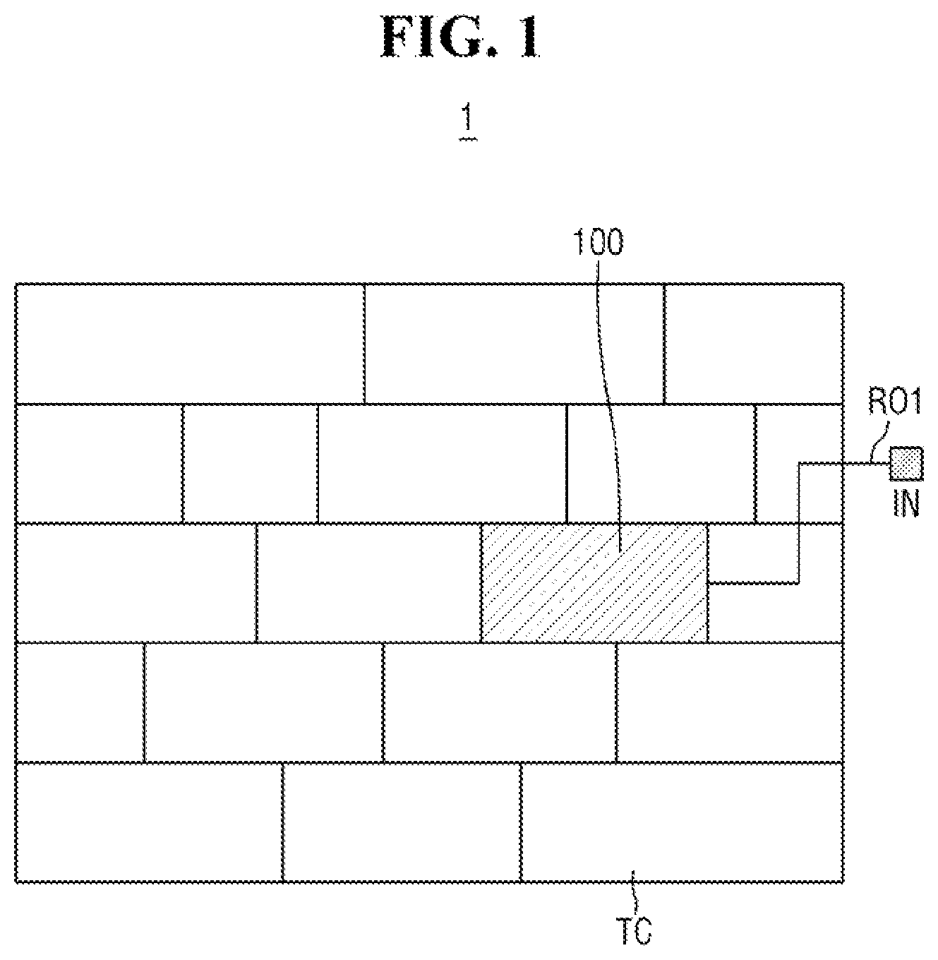
is a conceptual diagram of a semiconductor device according to some embodiments.
is a circuit diagram of a diode buffer cell of .
is a circuit diagram of a diode of .
is a layout of a diode buffer cell of .
is a layout of a region I of .
is a layout of a region II of .
is a cross-sectional view taken along line A-A′ of .
illustrates a connection relationship between wirings in a layout of .
illustrates a semiconductor device according to some embodiments.
is a circuit diagram of a diode buffer cell of a semiconductor device according to some embodiments.
illustrates a layout of a semiconductor device diode buffer cell according to some embodiments.
illustrates a layout of a region I of .
is a circuit diagram of a diode buffer cell of a semiconductor device according to some embodiments.
illustrates a layout of a diode buffer cell of a semiconductor device according to some embodiments.
illustrates a layout of a region I of .
DETAILED DESCRIPTION
Hereinafter, embodiments based on the technical idea of the present disclosure will be described with reference to the accompanying drawings.
is a conceptual diagram of a semiconductor device according to some embodiments.
Referring to , in some embodiments, a semiconductor device 1 includes a plurality of cells. At least one of the plurality of cells in the semiconductor device 1 is a diode buffer cell 100 . That is, the semiconductor device 1 includes at least one diode buffer cell 100 .
In some embodiments, the diode buffer cell 100 includes a buffer that stores data and a diode that prevents an antenna effect. That is, in the semiconductor device 1 according to a present embodiment, the buffer cell and the diode cell are not implemented by being separated into separate cells, but rather the buffer and the diode are integrated and implemented in a single cell.
In some embodiments, a routing wiring RO 1 connects an input terminal IN to which an input signal is provided and the diode buffer cell 100 .
Further, in some embodiments, the semiconductor device 1 includes at least one tap cell Tc. The tap cell TC may be spaced apart from the diode buffer cell 100 , as shown, or may be placed adjacent to the diode buffer cell 100 .
In some embodiments, the tap cell TC grounds a substrate placed in the diode buffer cell 100 . That is to say, if a substrate is placed over the diode buffer cell 100 and the tap cell TC, the substrate is grounded inside the tap cell TC, which is located outside the diode buffer cell 100 , rather than inside the diode buffer cell 100 . A substrate placed in the diode buffer cell 100 may also be grounded due to such a tap cell TC.
Hereinafter, the diode buffer cell 100 according to some embodiments will be described referring to to 8 .
is a circuit diagram of a diode buffer cell of . is a circuit diagram of a diode of . is a layout of a diode buffer cell of . is a layout of a region I of . is a layout of a region II of . is a cross-sectional view taken along line A-A′ of . illustrates a connection relationship between wirings in a layout of .
First, referring to , in some embodiments, the diode buffer cell 100 includes a diode 110 and a buffer 120 .
In some embodiments, the buffer 120 includes a first inverter that includes a transistor P 1 and a transistor N 1 , and a second inverter that includes a transistor P 2 and a transistor N 2 . However, embodiments are not limited thereto, and in other embodiments, the buffer can include more inverters than those shown.
In some embodiments, the sizes of the transistor P 2 and the transistor N 2 are greater than the sizes of the transistor P 1 and the transistor N 1 . Therefore, the drive strength of the second inverter is greater than the drive strength of the first inverter.
In some embodiments, the diode 110 is placed to prevent an antenna effect. The operation of a diode will be more specifically described below.
Referring to to 8 , in some embodiments, active regions ACT 1 and ACT 2 are formed on the substrate SUB inside the diode buffer cell 100 .
The substrate SUB may be bulk silicon or SOI (silicon-on-insulator). Alternatively, the substrate SUB may be a silicon substrate or may include other substances, such as silicon germanium, SGOI (silicon germanium on insulator), indium antimonide, lead tellurium compounds, indium arsenide, phosphide indium, gallium arsenide or gallium antimonide. However, embodiments of the technical idea of the present disclosure are not limited thereto.
In some embodiments, the active region ACT 1 and the active region ACT 2 are separated from each other in a second direction DR 2 .
In some embodiments, each of the active region ACT 1 and the active region ACT 2 protrudes from the substrate SUB in a third direction perpendicular to a first direction DR 1 that crosses the second direction DR 2 and the second direction DR 2 . Each of the active region ACT 1 and the active region ACT 2 is defined by an element isolation region. For example, the element isolation region is disposed on an element isolation trench formed between the active region ACT 1 and the active region ACT 2 .
In some embodiments, a first fin type pattern that intersects the active region ACT 1 and extends in the first direction DR 1 is disposed on the active region ACT 1 . The first fin type pattern protrudes from the active region ACT 1 in the third direction.
Further, in some embodiments, a second fin type pattern that intersects the active region ACT 2 and extends in the first direction DR 1 is disposed on the active region ACT 2 . The second fin type pattern protrudes from the active region Act 2 in the third direction.
In some embodiments, gate wirings G 1 to G 9 and dummy gate wirings DG 1 to DG 3 extend in the second direction DR 2 on the active region ACT 1 and the active region ACT 2 . The respective gate wirings G 1 to G 9 and the dummy gate wirings DG 1 to DG 3 are separated from each other in the first direction DR 1 .
In some embodiments, the gate wirings G 1 to G 9 include a conductor. The gate wiring G 1 to G 9 include, for example, at least one of titanium nitride (TiN), tantalum carbide (TaC), tantalum nitride (TaN), titanium silicon nitride (TiSiN), tantalum silicon nitride (TaSiN), tantalum titanium nitride (TaTiN), titanium aluminum nitride (TiAlN), tantalum aluminum nitride (TaAlN), tungsten nitride (WN), ruthenium (Ru), titanium aluminum (TiAl), titanium aluminum carbonitride (TiAlC—N), titanium aluminum carbide (TiAlC), titanium carbide (TiC), tantalum carbonitride (TaCN), tungsten (W), aluminum (Al), copper (Cu), cobalt (Co), titanium (Ti), tantalum (Ta), nickel (Ni), platinum (Pt), nickel platinum (Ni—Pt), niobium (Nb), niobium nitride (NbN), niobium carbide (NbC), molybdenum (Mo), molybdenum nitride (MoN), molybdenum carbide (MoC), tungsten carbide (WC), rhodium (Rh), palladium (Pd), iridium (Ir), osmium (Os), silver (Ag), gold (Au), zinc (Zn), or vanadium (V), or combinations thereof. The gate wirings G 1 to G 9 may include a conductive metal oxide, a conductive metal oxynitride, etc., and may include an oxidized form of the above-mentioned substances.
In some embodiments, the dummy gate wirings DG 1 to DG 3 include different substances from the gate wirings G 1 to G 9 . In some embodiments, the dummy gate wiring DG 1 to DG 3 may include polysilicon or an insulator, however, embodiments are not limited thereto.
In addition, in some embodiments, the dummy gate wirings DG 1 to DG 3 include the same substances as the gate wirings G 1 to G 9 .
In some embodiments, the dummy gate wirings DG 1 to DG 3 do not function as gate electrodes of the transistor, unlike the gate wirings G 1 to G 9 .
Referring to , in some embodiments, a gate insulating film G 1 is disposed below the gate wirings G 1 to G 9 and the dummy gate wirings DG 1 to DG 3 . The gate insulating film G 1 includes, for example, at least one of silicon oxide, silicon oxynitride, silicon nitride or a high dielectric constant material that has a higher dielectric constant than silicon oxide. The high dielectric constant materials include, for example, at least one of hafnium oxide, hafnium silicon oxide, hafnium aluminum oxide, lanthanum oxide, lanthanum aluminum oxide, zirconium oxide, zirconium silicon oxide, tantalum oxide, titanium oxide, barium strontium titanium oxide, barium titanium oxide, strontium titanium oxide, yttrium oxide, aluminum oxide, lead scandium tantalum oxide or lead zinc niobate.
In some embodiments, the gate insulating film G 1 extends to the top along the side wall of a spacer SP disposed on the side surfaces of the gate wirings G 1 to G 9 and the dummy gate wirings DG 1 to DG 3 .
In some embodiments, the spacer SP include, for example, at least one of silicon nitride (SiN), silicon oxynitride (SiON), silicon oxide (SiO 2 ), silicon carbonitride (SiCN), silicon oxycarbonitride (SiOCN), silicon boronitride (SiBN), silicon oxyboronitride (SiOBN), or silicone oxycarbide (SiOC), or combinations thereof. In some embodiments, the spacer SP has an L shape.
Referring to to 8 , impurity regions SD 10 to SD 19 are disposed in the active region ACT 1 , and impurity regions SD 20 to SD 29 are disposed in the active region ACT 2 . The impurity regions SD 10 to SD 19 and SD 20 to SD 29 function as a source or drain of a transistor.
In some embodiments, the active region ACIl includes n-type impurities, and the impurity regions SD 10 to SD 19 include p-type impurities or impurities that prevent diffusion of p-type impurities. As a result, the gate wirings G 1 to G 9 and the impurity regions SD 10 to SD 19 form a plurality of PMOS transistors. The impurity regions SD 10 to SD 19 include, for example, at least one of B, C, In, Ga, or Al, or a combination thereof, however, embodiments are not limited thereto.
In some embodiments, the active region ACT 2 includes p-type impurities, and the impurity regions SD 20 to SD 29 include n-type impurities or an impurity that prevents diffusion of n-type impurities. As a result, the gate wirings G 1 to G 9 and the impurity regions SD 20 to SD 29 form a plurality of NMOS transistors. The impurity regions SD 20 to SD 29 include, for example, at least one of P. Sb, or As, or a combination thereof, however, embodiments are not limited thereto.
shows an embodiment in which the impurity regions SD 10 to SD 19 and the impurity regions SD 20 to SD 29 are a single film, however, embodiments of the technical idea of the present disclosure are not limited thereto. In other embodiments, the impurity regions SD 10 to SD 19 and the impurity regions SD 20 to SD 29 are formed of multi-layer films that contain impurities of different concentrations from each other.
In some embodiments, a wiring M 11 extends in the first direction DR 1 . A power supply voltage VDD is transmitted to the wiring M 11 .
In some embodiments, the wiring M 11 is connected to the impurity regions SD 10 , SD 11 , SD 12 , SD 13 , SD 15 , SD 17 , and SD 19 . Specifically, the wiring M 11 is connected to the impurity region SD 10 through a contact CT 11 , connected to the impurity region SD 11 through a contact CT 12 , and connected to the impurity region SD 12 through a contact CT 13 . Further, the wiring M 11 is connected to the impurity region SD 13 through a contact CT 14 , connected to the impurity region SD 15 through a contact CT 15 , connected to the impurity region SD 17 through a contact CT 16 , and connected to the impurity region SD 19 through the contact CT 17 . Accordingly, the power supply voltage VDD may be applied to the impurity regions SD 10 , SD 11 , SD 12 , SD 13 , SD 15 , SD 17 , and SD 19 through the wiring MI I.
In some embodiments, a wiring M 12 extends in the first direction DR 1 . The wiring M 12 is grounded GND.
In some embodiments, the wiring M 12 is connected to the impurity regions SD 23 , SD 25 , SD 27 , and SD 29 . Specifically, the wiring M 12 is connected to the impurity region SD 23 through a contact CT 51 , connected to the impurity region SD 25 through a contact CT 52 , connected to the impurity region SD 27 through a contact CT 53 , and connected to the impurity region SD 29 through a contact CT 54 . Therefore, the impurity regions SD 23 , SD 25 , SD 27 , and SD 29 are grounded through the wiring M 12 .
On the other hand, in some embodiments, the impurity regions SD 20 , SD 21 and SD 22 are not connected to the wiring M 12 . That is, the impurity regions SD 20 , SD 21 and SD 22 are not grounded through the wiring M 12 .
In some embodiments, a wiring M 13 is connected to an input terminal IN. Accordingly, an input signal can be transmitted from the input terminal IN through the wiring M 13 .
In some embodiments, the wiring M 13 is placed higher than the gate wirings G 1 to G 9 and the dummy gate wirings DG 1 to DG 3 . Specifically, the wiring M 13 extends in the first direction DR 1 , and overlaps the gate electrodes G 1 to G 4 and the dummy gate electrodes DG 1 and DG 2 .
In some embodiments, the wiring M 13 is connected to the gate wiring G 2 , the gate wiring G 3 , and the gate wiring G 4 . Specifically, the wiring M 13 is connected to the gate wiring G 2 through a contact CT 31 , connected to the gate wiring G 3 through a contact CT 32 , and connected to the gate wiring G 4 through a contact. CT 33 .
In some embodiments, a wiring M 4 is connected to the impurity regions SD 20 , SD 21 and SD 22 . Specifically, the wiring M 14 is connected to the impurity region SD 20 through a contact CT 41 , connected to the impurity region SD 21 through a contact CT 42 , and connected to the impurity region SD 22 through a contact CT 43 .
In some embodiments, the wiring M 14 is placed at substantially the same height as the wiring M 13 . That is, the wiring M 14 is placed higher than the gate wirings G 1 to G 9 and the dummy gate wirings DG to DG 3 . Specifically, the wiring M 14 extends in the first direction DR 1 , and overlaps the gate electrodes G 1 to G 3 and the dummy gate electrode DG 1 .
In some embodiments, a wiring M 15 connects the impurity region SD 14 and the impurity region SD 24 with the gate wirings G 6 , G 7 , and G 8 . Specifically, the wiring M 15 is connected to the impurity region SD 14 through a contact CT 21 , connected to the impurity region SD 24 through a contact CT 44 , connected to the gate wiring G 6 through a contact CT 34 , connected to the gate wiring G 7 through a contact CT 35 , and connected to the gate wiring G 7 through a contact CT 36 . The wiring M 15 transmits the output of the aforementioned first inverter to the second inverter.
In some embodiments, a wiring M 16 connects the impurity region SD 16 , the impurity region SD 18 , the impurity region SD 26 , and the impurity region SD 28 to the wiring M 22 . Specifically, the wiring M 16 is connected to the impurity region SD 16 through a contact CT 22 , connected to the impurity region SD 18 through a contact CT 23 , connected to the impurity region SD 26 through a contact CT 42 , connected to the impurity region SD 28 through a contact CT 42 , and connected to the wiring M 22 through a via V 3 . The wiring M 16 transmits the output of the aforementioned second inverter to an output terminal OUT connected to the wiring M 22 .
In some embodiments, the wiring M 13 , the wiring M 15 and the wiring M 16 are placed at substantially the same height.
In some embodiments, the wiring M 22 is placed higher than the wiring M 13 , the wiring M 15 and the wiring M 16 . The wiring M 22 is connected to the output terminal OUT.
In some embodiments, a wiring M 21 is placed higher than the wiring M 13 and the wiring M 14 . The wiring M 21 extends in the second direction DR 2 . The wiring M 21 is connected to the wiring M 13 by a via V 1 and is connected to the wiring M 14 by a via V 2 .
In some embodiments, an interlayer insulating film ILD is disposed between the wirings, contacts and vias. The interlayer insulating film ILD includes, for example, at least one of silicon oxide, silicon oxynitride or a low dielectric constant (low-k) material that has a lower dielectric constant than silicon oxide, however, embodiments are not limited thereto.
In some embodiments, a diode 110 is disposed in the first region I, and a buffer 120 is disposed in the second region II
In some embodiments, the buffer 120 includes a first inverter that includes the gate wiring G 4 and the impurity region SD 13 , SD 14 , SD 23 , and SD 24 , and a second inverter that includes the gate wirings G 6 , G 7 , and G 8 and the impurity regions SD 15 to SD 18 and SD 25 to 28 . In a present embodiment, since the drive strength of the second inverter is greater than the drive strength of the first inverter, a width W 2 of the wiring M 16 in the second direction DR 2 is greater than a width W 1 of the wiring M 15 in the second direction DR 2 .
In some embodiments, the first region I and the second region II are divided into two dummy gate wirings DG 1 and DG 2 . An isolation region DF that divides the first region I and the second region II is disposed below each of the two dummy gate wirings DG 1 and DG 2 .
Although the drawing shows an example in which two dummy gate wirings DG 1 and DG 2 are placed between the first region I and the second region II, embodiments are not limited thereto. In some embodiments, one dummy gate wiring and the isolation region are disposed between the first region I and the second region II to divide the first region I and the second region II.
Referring to , 5 and 7 , in some embodiments, the substrate SUB in which the active region ACT 2 is placed is grounded by tap cell TC as described above. Further, in the diode buffer cell 100 , the active region ACT 2 , and the impurity regions SD 20 , SD 21 , and SD 22 are not grounded. Accordingly, the p-type active region ACT 2 and the n-type impurity regions SD 20 , SD 21 , and SD 22 function as the diode. That is to say, since the active region ACT 2 , the substrate SUB, and the impurity regions SD 20 , SD 21 , and SD 22 function as a diode between the wirings M 13 , an antenna effect in which charge accumulates in the wiring M 13 and other wirings connected to the wiring M 13 from the substrate SUB is prevented.
illustrates an effect of a semiconductor device according to some embodiments.
Specifically, illustrates a semiconductor device 99 in which a buffer cell BC and a diode cell DC are separated. As described above, the diode cell DC to the buffer cell BC should be connected to eliminate the antenna effect. However, as shown, when the buffer cell BC and the diode cell DC are placed separately, a plurality of routing wirings RO 2 and RO 3 are needed, which increases the complexity of the design.
However, in a present embodiment, since the p-type active region ACT 2 and the n-type impurity regions SD 20 , SD 21 , and SD 22 placed between the substrate SUB and the wiring M 13 are used as a diode to embody both the diode and the buffer in a single cell, a semiconductor device can be provided with easy routing and improved product reliability.
Hereinafter, a diode buffer cell of a semiconductor device according to some embodiments will be described referring to to 12 .
is a circuit diagram of the diode buffer cell of a semiconductor device according to some embodiments. illustrates a layout of a semiconductor device diode buffer cell according to some embodiments. illustrates a layout of a region I of .
Hereinafter, repeated description of features described above will be omitted and differences will be mainly described.
Referring to to 12 , in some embodiments, a diode buffer cell 200 includes a diode 210 and a buffer 220 .
In a present embodiment, the wiring M 13 of the diode buffer cell 200 is not connected to the gate wiring G 2 and the gate wiring G 3 .
In some embodiments, although the wiring M 13 is connected to the gate wiring G 2 through the contact CT 31 , and connected to the gate wiring G 3 through the contact CT 32 in an above-described embodiment, the contacts CT 31 and CT 32 described above are not present in an embodiment of to 12 . Accordingly, the gate wiring G 2 and the gate wiring G 3 floats by not being connected to the wiring M 13 . Accordingly, an input capacitance is reduced.
Hereinafter, a diode buffer cell of a semiconductor device according to some embodiments will be described referring to 15 .
is a circuit diagram of a diode buffer cell of a semiconductor device according to some embodiments. illustrates a layout of a diode buffer cell of a semiconductor device according to some embodiments. illustrates a layout of a region I of .
Hereinafter, repeated description of the features described above will be omitted and differences will be mainly described.
Referring to to 15 , in some embodiments, a diode buffer cell 300 includes a diode 310 and a buffer 320 .
In some embodiments, the diode buffer cell 300 further includes a wiring M 17 connected to the impurity regions SD 10 , SD 11 , and SD 12 . That is, unlike an above-described embodiment, the impurity regions SD 10 , SD 11 , and SD 12 of the diode buffer cell 300 according to a present embodiment are not connected to the wiring M 11 that receives the power supply voltage VDD.
In some embodiments, the wiring M 17 is connected to the impurity region SD 10 through the contact CT 24 , connected to the impurity region SD 11 through the contact CT 25 , and connected to the impurity region SD 12 through the contact CT 26 .
In some embodiments, the wiring M 17 is disposed at substantially the same height as the wiring M 13 . That is, the wiring M 17 is disposed higher than the gate wirings G 1 to G 9 and the dummy gate wirings DG 1 to DG 3 . Specifically, the wiring M 17 extends in the first direction DR 1 , and overlaps the gate electrodes G 1 to G 3 and the dummy gate electrode DG 1 .
In some embodiments, the wiring M 21 are placed higher than the wiring M 13 , the wiring M 14 and the wiring M 17 . The wiring M 21 extends in the second direction DR 2 . The wiring M 21 is connected to the wiring M 13 by the vias V 1 , connected to the wiring M 14 by the via V 2 , and connected to the wiring M 17 by a via V 4 .
In some embodiments, the impurity regions SD 10 , SD 11 and SD 12 , and the impurity regions SD 20 , SD 21 and SD 22 are connected to each other by the wiring M 13 , the wiring M 21 , the wiring M 14 , and the wiring M 17 . Further, the impurity regions SD 10 , SD 11 , and SD 12 and the impurity regions SD 20 , SD 21 , and SD 22 are connected to the input terminal IN through the wiring M 13 .
In some embodiments, the wiring M 13 is not connected to the gate wiring G 2 and the gate wiring G 3 . Accordingly, the gate wiring G 2 and the gate wiring G 3 floats by not being connected to the wiring M 13 .
In concluding the detailed description, those skilled in the art will appreciate that many variations and modifications may be made to embodiments without substantially departing from the principles of the present disclosure. Therefore, disclosed embodiments of the disclosure are used in a generic and descriptive sense only and not for purposes of limitation.
Figures (14)
Citations
This patent cites (129)
- US5072286
- US5414292
- US6043699
- US6366113
- US6400206
- US6414359
- US6502229
- US6885609
- US6974978
- US7112996
- US7208979
- US7262651
- US7302663
- US7388410
- US7394155
- US7410843
- US7554361
- US7764475
- US7880501
- US7915691
- US7924604
- US8063415
- US8143653
- US8194371
- US8243403
- US8357955
- US8446175
- US8595661
- US8679911
- US8741763
- US8847329
- US9122832
- US9142556
- US9245081
- US9318607
- US9460259
- US9502351
- US9589955
- US9613714
- US9646711
- US9646960
- US9698056
- US9773772
- US9831877
- US9875791
- US10050032
- US10128255
- US10270430
- US10515943
- US10541237
- US10573634
- US10600785
- US10943923
- US11024620
- US11050424
- US11322443
- US11424251
- US11539206
- US11557582
- US11632101
- US2003/0200071
- US2004/0174201
- US2004/0207450
- US2005/0024088
- US2005/0138598
- US2006/0170052
- US2007/0001197
- US2007/0162880
- US2007/0241810
- US2008/0036522
- US2009/0026546
- US2009/0189670
- US2010/0187609
- US2010/0277622
- US2011/0025734
- US2012/0146988
- US2013/0026571
- US2013/0026572
- US2013/0329487
- US2014/0027918
- US2014/0217513
- US2014/0223395
- US2015/0014775
- US2016/0118090
- US2016/0285452
- US2017/0053696
- US2017/0093401
- US2017/0103699
- US2017/0125360
- US2017/0133367
- US2017/0170075
- US2017/0222649
- US2017/0294430
- US2017/0330614
- US2018/0108646
- US2018/0158811
- US2018/0166119
- US2018/0183414
- US2018/0294812
- US2018/0342494
- US2018/0342505
- US2019/0065659
- US2019/0067263
- US2019/0148407
- US2019/0198507
- US2019/0198529
- US2019/0214394
- US2019/0393205
- US2019/0393877
- US2020/0050731
- US2020/0051611
- US2020/0059228
- US2020/0075478
- US2020/0143876
- US2020/0144245
- US2020/0152627
- US2021/0104463
- US2021/0104611
- US2021/0225425
- US2022/0020738
- US2022/0084959
- US2022/0108989
- US2022/0238081
- US2022/0246623
- US2022/0270969
- US2022/0293584
- US2023/0027769
- US2023/0100170
- US10-2019-0076874