Multiple-reference-embedded Comparator and Comparison Method Thereof
Abstract
A multiple-reference-embedded comparator (MREC) circuit includes a tail current source circuit; an input transistor pair, coupled to the tail current source circuit, configured to receive differential input voltages and perform a first pre-amplification to generate first differential amplified voltages according to the differential input voltages; and a plurality of embedded reference (ER) branches, each coupled to the input transistor pair, each configured to perform a second pre-amplification to generate second differential amplified voltages according to the first differential amplified voltages, and to perform a discrete-time comparison to generate differential output voltages according to the second differential amplified voltages.
Claims (8)
1. A multiple-reference-embedded comparator (MREC) circuit, comprising: a tail current source circuit; an input transistor pair, coupled to the tail current source circuit, configured to receive differential input voltages and perform a first pre-amplification to generate first differential amplified voltages according to the differential input voltages; and a plurality of embedded reference (ER) circuits, each coupled to the input transistor pair, each configured to perform a second pre-amplification to generate second differential amplified voltages according to the first differential amplified voltages, and to perform a discrete-time comparison to generate differential output voltages according to the second differential amplified voltages; wherein each of the plurality of ER circuits comprises: an adjustor circuit, coupled to the input transistor pair, configured to perform the second pre-amplification to generate the second differential amplified voltages according to the first differential amplified voltages and differential bias voltages; and a latch circuit, coupled to the adjustor circuit, configured to perform the discrete-time comparison to generate the differential output voltages according to the second differential amplified voltages.
5. A comparison method for a multiple-reference-embedded comparator (MREC) circuit, comprising: utilizing an input transistor pair, coupled to a tail current source circuit, to perform a first pre-amplification to generate first differential amplified voltages according to differential input voltages; and utilizing each of a plurality of embedded reference (ER) circuits, each coupled to the input transistor pair, to perform a second pre-amplification to generate second differential amplified voltages according to the first differential amplified voltages, and to perform a discrete-time comparison to generate differential output voltages according to the second differential amplified voltages; wherein each of the plurality of ER circuits comprises: an adjustor circuit, coupled to the input transistor pair, configured to perform the second pre-amplification to generate the second differential amplified voltages according to the first differential amplified voltages and differential bias voltages; and a latch circuit, coupled to the adjustor circuit, configured to perform the discrete-time comparison to generate the differential output voltages according to the second differential amplified voltages.
Show 6 dependent claims
2. The MREC circuit of claim 1 , wherein the input transistor pair comprises: a first field-effect transistor, comprising a first drain, a first gate and a first source; and a second field-effect transistor, comprising a second drain, a second gate and a second source; wherein the first source and the second source are coupled to the tail current source circuit; the first gate and the second gate are configured to receive the differential input voltages; and the first drain and the second drain are coupled to the plurality of ER circuits to output the first differential amplified voltages.
3. The MREC circuit of claim 1 , wherein the adjustor circuit comprises: a third field-effect transistor, comprising a third drain, a third gate and a third source; and a fourth field-effect transistor, comprising a fourth drain, a fourth gate and a fourth source; wherein the third source and the fourth source receive the first differential amplified voltages respectively; the third gate and the fourth gate receive the differential bias voltages respectively; and the third drain and the third drain are coupled to the latch circuit to output the second differential amplified voltages.
4. The MREC circuit of claim 1 , wherein the latch circuit comprises: a fifth field-effect transistor, comprising a fifth drain, a fifth gate and a fifth source; a sixth field-effect transistor, comprising a sixth drain, a sixth gate and a sixth source; a seventh field-effect transistor, comprising a seventh drain, a seventh gate and a seventh source; and an eighth field-effect transistor, comprising an eighth drain, an eighth gate and an eighth source; wherein the fifth source and the sixth source receive the second differential amplified voltages respectively; the seventh source and the eighth source are coupled to a supply voltage; the fifth gate, the seventh gate, the sixth drain and the eight drain are coupled to a first output node; and the sixth gate, the eighth gate, the fifth drain and the seventh drain are coupled to a second output node; wherein the first output node and the second output node output the differential output voltages.
6. The comparison method of claim 5 , wherein the input transistor pair comprises: a first field-effect transistor, comprising a first drain, a first gate and a first source; and a second field-effect transistor, comprising a second drain, a second gate and a second source; wherein the first source and the second source are coupled to the tail current source circuit; the first gate and the second gate are configured to receive the differential input voltages; and the first drain and the second drain are coupled to the plurality of ER circuits to output the first differential amplified voltages.
7. The comparison method of claim 5 , wherein the adjustor circuit comprises: a third field-effect transistor, comprising a third drain, a third gate and a third source; and a fourth field-effect transistor, comprising a fourth drain, a fourth gate and a fourth source; wherein the third source and the fourth source receive the first differential amplified voltages respectively; the third gate and the fourth gate receive the differential bias voltages respectively; and the third drain and the third drain are coupled to the latch circuit to output the second differential amplified voltages.
8. The comparison method of claim 5 , wherein the latch circuit comprises: a fifth field-effect transistor, comprising a fifth drain, a fifth gate and a fifth source; a sixth field-effect transistor, comprising a sixth drain, a sixth gate and a sixth source; a seventh field-effect transistor, comprising a seventh drain, a seventh gate and a seventh source; and an eighth field-effect transistor, comprising an eighth drain, an eighth gate and an eighth source; wherein the fifth source and the sixth source receive the second differential amplified voltages respectively; the seventh source and the eighth source are coupled to a supply voltage; the fifth gate, the seventh gate, the sixth drain and the eight drain are coupled to a first output node; and the sixth gate, the eighth gate, the fifth drain and the seventh drain are coupled to a second output node; wherein the first output node and the second output node output the differential output voltages.
Full Description
Show full text →
BACKGROUND OF THE INVENTION
1. Field of the Invention
The present invention relates to a comparator circuit and a comparison method thereof, and more particularly, to a multiple-reference-embedded comparator circuit and a comparison method thereof.
2. Description of the Prior Art
Analog-to-digital converters (ADCs) typically require a large number of comparators to quickly complete data quantization and achieve a high-speed specification. However, the comparators may give rise to high power consumption and high circuitry cost. For example, a typical dynamic comparator includes a tail current source, an input differential pair and a latch. Thus, using multiple dynamic comparators (including multiple tail current sources, multiple input differential pairs and multiple latches) results in a substantial power consumption of the ADC and generates a great amount of heat that degrades ADC performance. In addition, a resistor ladder used to provide reference voltages to the dynamic comparators also results in a large power consumption. On the other hand, kickback errors and parasitic capacitances attributed to the input differential pair also degrade the ADC performance.
Therefore, how to improve the dynamic comparators to have a low power consumption and make the ADC to have high accuracy with a small circuit area has become one of the goals in the industry.
SUMMARY OF THE INVENTION
The present invention is to provide a multiple-reference-embedded comparator circuit and a comparison method with multiple references embedded.
The present invention provides a multiple-reference-embedded comparator (MREC) circuit, comprising a tail current source circuit; an input transistor pair, coupled to the tail current source circuit, configured to receive differential input voltages and perform a first pre-amplification to generate first differential amplified voltages according to the differential input voltages; and a plurality of embedded reference (ER) branches, each coupled to the input transistor pair, each configured to perform a second pre-amplification to generate second differential amplified voltages according to the first differential amplified voltages, and to perform a discrete-time comparison to generate differential output voltages according to the second differential amplified voltages.
The present invention provides a comparison method for a multiple-reference-embedded comparator (MREC) circuit, comprising utilizing an input transistor pair, coupled to a tail current source circuit, to perform a first pre-amplification to generate first differential amplified voltages according to differential input voltages; and utilizing each of a plurality of embedded reference (ER) branches, each coupled to the input transistor pair, to perform a second pre-amplification to generate second differential amplified voltages according to the first differential amplified voltages, and to perform a discrete-time comparison to generate differential output voltages according to the second differential amplified voltages.
These and other objectives of the present invention will no doubt become obvious to those of ordinary skill in the art after reading the following detailed description of the preferred embodiment that is illustrated in the various figures and drawings.
BRIEF DESCRIPTION OF THE DRAWINGS
is a schematic diagram of a multiple-reference-embedded comparator (MREC) circuit according to an embodiment of the present invention.
is a flow chart of a comparison method according to an embodiment of the present invention.
is a schematic diagram of a MREC circuit with a single ER branch according to an embodiment of the present invention.
is waveform diagrams of the first differential amplified voltages, the second differential amplified voltages, and the differential output voltages of the embodiment of the present invention.
is a schematic diagram of a MREC circuit with three ER branches according to an embodiment of the present invention.
is waveform diagrams of the first differential amplified voltages, the second differential amplified voltages of the three ER branches of the embodiment of the present invention.
DETAILED DESCRIPTION
Certain terms used throughout the description and following claims to refer to particular components. As one skilled in the art will appreciate, hardware manufacturers may refer to a component by different names. This document does not intend to distinguish between components that differ in name but not function. In the following description and in the claims, the terms “include” and “comprise” are utilized in an open-ended fashion, and thus should be interpreted to mean “include, but not limited to”. Also, the term “couple” is intended to mean either an indirect or direct electrical connection. Accordingly, if one device is coupled to another device, that connection may be through a direct electrical connection, or through an indirect electrical connection via other devices and connections.
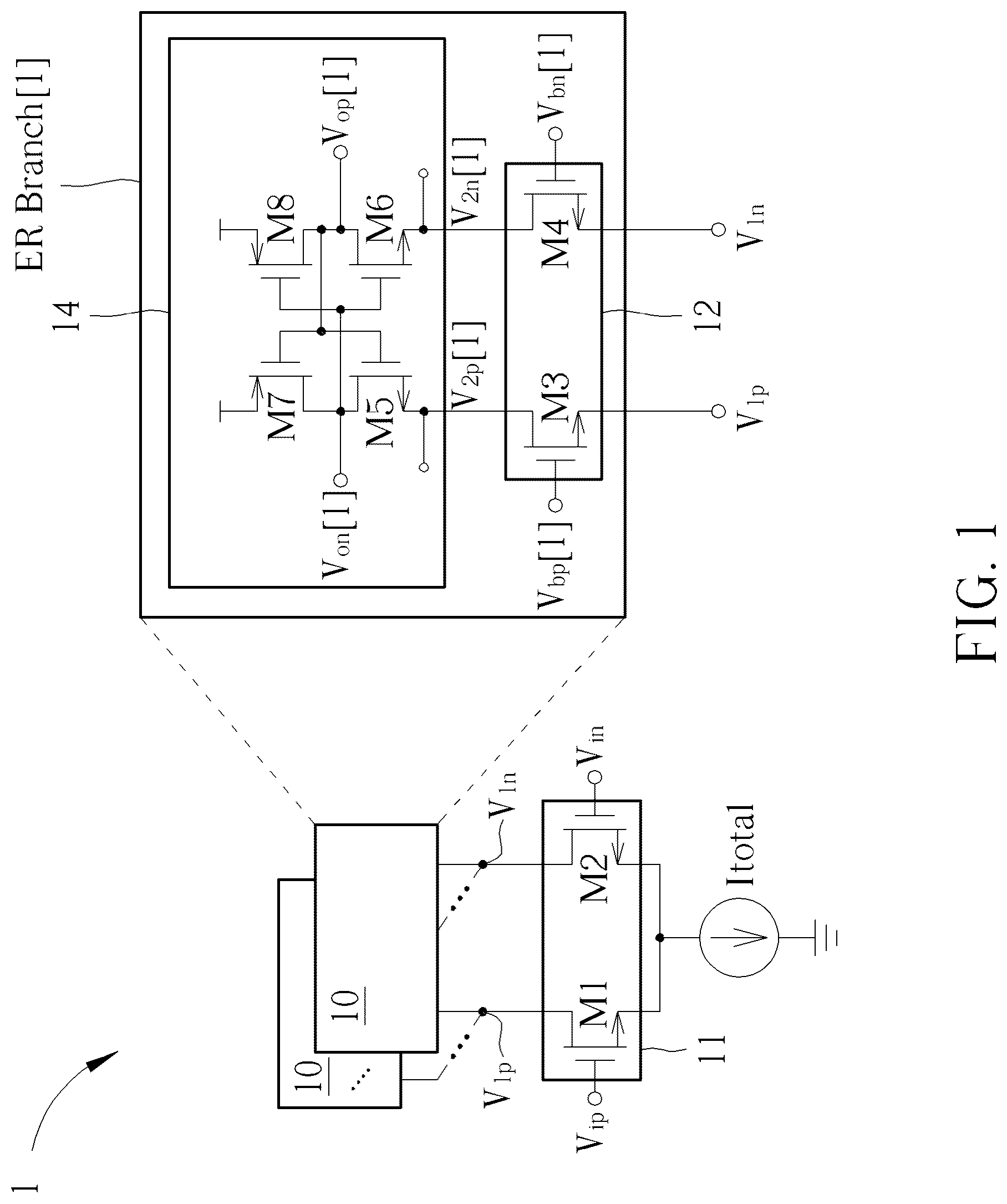
Please refer to . is a schematic diagram of a multiple-reference-embedded comparator (MREC) circuit 1 according to an embodiment of the present invention. The MREC circuit 1 includes a tail current source circuit I total , an input transistor pair 11 (M 1 +M 2 ), and a plurality of embedded reference (ER) branches 10 . The input transistor pair 11 is coupled to the tail current source circuit I total , and is configured to receive differential input voltages V ip and V in . Each of the plurality of ER branches 10 is coupled to the input transistor pair 11 , and is configured to generate and output differential output voltages V on and V op as a comparison result according to the differential input voltages V ip and V in . This allows n ER branches sharing the differential pair 11 and the tail current source I total to generate n comparison results, denoted as V op [ 1 ], V on [ 1 ] to V op [n], V on [n], where n≥2. For example, as shown in , a first ER branch of the ER branches generates and outputs a first comparison result as the differential output voltages V on [ 1 ] and V op [ 1 ].
In detail, a comparison method for the MREC circuit 1 may be summarized as a flow 2 , as shown in . It should be noted that the operations of the plurality of ER branches are similar, so only the first ER branch is described. The flow 2 includes the following steps:
Step S 200 : Perform a first pre-amplification.
Step S 202 : Perform a second pre-amplification.
Step S 204 : Perform a discrete-time comparison.
In step S 200 , the input transistor pair M 1 and M 2 receives the differential input voltages V ip and V in and performs the first pre-amplification PA 1 to generate first differential amplified voltages V ip and V in according to the differential input voltages V ip and V in .
In step S 202 , the first ER branch includes an adjustor 12 and a latch circuit 14 . The adjustor 12 is coupled between the input transistor pair 11 and the latch circuit 14 . The adjustor 12 receives the first differential amplified voltages V ip and V in and performs the second pre-amplification PA 2 to generate the second differential amplified voltages V 2p [ 1 ] and V 2n [ 1 ] according to the first differential amplified voltages V ip and V in and differential bias voltages V bp [ 1 ] and V bn [ 1 ].
In step S 204 , the latch circuit 14 receives the second differential amplified voltages V 2p [ 1 ] and V 2n [ 1 ] and performs the discrete-time comparison to generate the differential output voltages V op [ 1 ] and V on [ 1 ] as the first comparison result according to the second differential amplified voltages V 2p [ 1 ] and V 2n [ 1 ].
Specifically, as shown in , the input transistor pair 11 includes a first field-effect transistor M 1 , including a first drain, a first gate and a first source, and a second field-effect transistor M 2 , including a second drain, a second gate and a second source. The first source and the second source are coupled to the tail current source circuit I total ; the first gate and the second gate are configured to receive the differential input voltages V ip and V in ; and the first drain and the second drain are coupled to the plurality of ER branches to output the first differential amplified voltages V ip and V in .
On the other hand, the adjustor 12 includes a third field-effect transistor M 3 , including a third drain, a third gate and a third source, and a fourth field-effect transistor M 4 , including a fourth drain, a fourth gate and a fourth source. The third source and the fourth source receive the first differential amplified voltages V ip and V in , respectively; the third gate and the fourth gate receive the differential bias voltages V bp [ 1 ] and V on [ 1 ], respectively; and the third drain and the third drain are coupled to the latch circuit 14 to output the second differential amplified voltages V 2p [ 1 ] and V 2n [ 1 ].
Furthermore, the latch circuit 14 includes a fifth field-effect transistor M 5 , including a fifth drain, a fifth gate and a fifth source, a sixth field-effect transistor M 6 , including a sixth drain, a sixth gate and a sixth source, a seventh field-effect transistor M 7 , including a seventh drain, a seventh gate and a seventh source, and an eighth field-effect transistor M 8 , including an eighth drain, an eighth gate and an eighth source. The fifth source and the sixth source receive the second differential amplified voltages V 2p [ 1 ] and V 2n [ 1 ], respectively; the seventh source and the eighth source are coupled to a supply voltage V DD ; the fifth gate, the seventh gate, the sixth drain and the eight drain are coupled to a first output node; and the sixth gate, the eighth gate, the fifth drain and the seventh drain are coupled to a second output node. The first output node and the second output node output the differential output voltages V op [ 1 ] and V on [ 1 ], respectively.
It should be noted that the circuit schematic diagram of the above-mentioned ER branch is only an embodiment of the present invention, and those skilled in the art may make appropriate adjustments according to the circuit requirements. The following description only shows the symbols for the adjustor 12 and the latch circuit 14 to illustrate the operation of the comparison method. Please refer to and . is a schematic diagram of an MREC circuit 3 with a single ER branch (the adjustor 12 and the latch circuit 14 ) according to an embodiment of the present invention. shows waveform diagrams of the first differential amplified voltages V ip and V in , the second differential amplified voltages V 2p and V an , and the differential output voltages V op and V on of the embodiment of the present invention. As shown in and , when the tail current source (Mc) is turned on (Φ turns to high), the MREC circuit 3 starts to operate. The input transistor pair 11 receives the differential input voltages V ip and V in and performs the first pre-amplification PA 1 to generate first differential amplified voltages V ip and V in . The adjustor 12 receives differential bias voltages V bp and V on and the first differential amplified voltages V ip and V in to perform the second pre-amplification PA 2 to generate the second differential amplified voltages V 2p and V 2n . Specifically, for the first pre-amplification PA 1 , the first drain and the second drain of the input transistor pair M 1 and M 2 are discharged from the supply voltage V DD toward (V bp -V th ) and (V bn -V th ), respectively, so that the adjustor 12 is turned on, where V th is a threshold voltage of the transistors. For the second pre-amplification PA 2 , the third drain and the fourth drain of the adjustor 12 are discharged from the supply voltage V DD toward a voltage drop as the threshold voltage V th , so that the latch circuit 14 is turned on. The latch circuit 14 receives the second differential amplified voltages V 2p and V an to generate differential output voltages V op and V on as the comparison result.
Please refer to and . is a schematic diagram of an MREC circuit 4 with three ER branches (ER branch[ 1 ], ER branch[ 2 ] and ER branch[ 3 ]) according to an embodiment of the present invention. shows waveform diagrams of the first differential amplified voltages V ip and V in , the second differential amplified voltages of the three ER branches of the embodiment of the present invention. As shown in and , when the tail current source (Mc) is turned on (Φ turns to high), the MREC circuit 4 starts to operate. The input transistor pair M 1 and M 2 receives the differential input voltages V ip and V in and performs the first pre-amplification PA 1 to generate first differential amplified voltages V ip and V in . A first adjustor circuit Adj 1 of the ER branch [ 1 ] receives differential bias voltages V bp [ 1 ] and V on [ 1 ] and the first differential amplified voltages V ip and V in to perform the second pre-amplification PA 2 to generate second differential amplified voltages V 2p [ 1 ] and V 2n [ 1 ]. By the same mechanism, a second adjustor circuit Adj 2 of the ER branch[ 2 ] performs the second pre-amplification PA 2 to generate second differential amplified voltages V 2p [ 2 ] and V an [ 2 ], and a third adjustor circuit Adj 3 of the ER branch[ 3 ] performs the second pre-amplification PA 2 to generate second differential amplified voltages V 2p [ 3 ] and V an [ 3 ]. Latch circuits latch 1 , latch 2 and latch 3 generate differential output voltages as three comparison results accordingly. In short, as shown in and , for the first pre-amplification PA 1 , the first drain and the second drain of the input transistor pair M 1 and M 2 are discharged from the supply voltage V DD toward (V bp -V th ) and (V bn -V th ), respectively, so that the adjustors Adj 1 , Adj 2 and Adj 3 are turned on. On the other hand, for the second pre-amplification PA 2 , the third drain and the fourth drain of the adjustors Adj 1 , Adj 2 and Adj 3 are discharged from the supply voltage V DD toward a voltage drop as the threshold voltage V th , so that the latch circuits latch 1 , latch 2 and latch 3 are turned on, respectively. The latch circuits latch 1 , latch 2 and latch 3 receive second differential amplified voltages V 2p/2n [ 1 ], V 2p/2n [ 2 ] and V 2p/2n [ 3 ] to generate differential output voltages V op/on [ 1 ], V op/on [ 2 ] and V op/on [ 3 ] as the comparison results, respectively.
In summary, in the embodiment of the present invention, the plurality of ER branches share a tail current source and an input differential transistor pair performing the first pre-amplification to perform the plurality of the second pre-amplification and the plurality of the discrete-time comparison. Therefore, compared with the prior art, the MREC circuit of the present invention achieves a low power consumption, and occupies a smaller circuit area.
Those skilled in the art will readily observe that numerous modifications and alterations of the device and method may be made while retaining the teachings of the invention. Accordingly, the above disclosure should be construed as limited only by the metes and bounds of the appended claims.
Figures (5)
Citations
This patent cites (3)
- US10917100
- US2019/0277891
- US2024/0063765