Frequency Calibration Circuit and Method for Calibrating Oscillation Frequency of Controllable Oscillator
Abstract
A frequency calibration (FCAL) circuit and a method for calibrating an oscillation frequency of a controllable oscillator are provided. The FCAL circuit includes the controllable oscillator, a divider, a time-to-digital converter (TDC) and a calibration logic. The controllable oscillator generates a controllable oscillation clock according to a calibration code. The divider divides the oscillation frequency of the controllable oscillation clock by a predetermined divisor to generate a divided clock. The TDC converts a first period between first edges of a reference clock and the divided clock into a first period code and converts a second period between second edges of the reference clock and the divided clock into a second period code. The calibration logic compares the first period code and the second period code to generate a comparison result for determining whether the first period is greater or less than the second period, and accordingly controls the calibration code.
Claims (19)
1. A frequency calibration (FCAL) circuit, comprising: a controllable oscillator, configured to generate a controllable oscillation clock according to a calibration code, wherein an oscillation frequency of the controllable oscillation clock is controlled according to the calibration code; a divider, coupled to the controllable oscillator, configured to divide the oscillation frequency of the controllable oscillation clock by a predetermined divisor to generate a divided clock; a time-to-digital converter (TDC), coupled to the divider, configured to convert a first period between a first edge of a reference clock and a first edge of the divided clock into a first period code and convert a second period between a second edge of the reference clock and a second edge of the divided clock into a second period code; and a calibration logic, coupled to the controllable oscillator and the TDC, configured to compare the first period code and the second period code to generate a comparison result for determining whether the first period is greater or less than the second period, and control the calibration code according to the comparison result.
10. A method for calibrating an oscillation frequency of a controllable oscillator, comprising: utilizing the controllable oscillator to generate a controllable oscillation clock according to a calibration code, wherein the oscillation frequency of the controllable oscillation clock is controlled according to the calibration code; utilizing a divider to divide the oscillation frequency of the controllable oscillation clock by a predetermined divisor to generate a divided clock; utilizing a time-to-digital converter (TDC) to convert a first period between a first edge of a reference clock and a first edge of the divided clock into a first period code and convert a second period between a second edge of the reference clock and a second edge of the divided clock into a second period code; and utilizing a calibration logic to compare the first period code and the second period code to generate a comparison result for determining whether the first period is greater or less than the second period, and control the calibration code according to the comparison result.
Show 17 dependent claims
2. The FCAL circuit of claim 1 , wherein the calibration logic is configured to control the calibration code to make the second period code approach the first period code.
3. The FCAL circuit of claim 1 , wherein when the comparison result indicates that the second period is less than the first period, the calibration logic switches the calibration code to reduce the oscillation frequency of the controllable oscillation clock; and when the comparison result indicates that the second period is greater than the first period, the calibration logic switches the calibration code to increase the oscillation frequency of the controllable oscillation clock.
4. The FCAL circuit of claim 1 , wherein the first edge of the divided clock and the second edge of the divided clock are edges respectively following the first edge of the reference clock and the second edge of the reference clock.
5. The FCAL circuit of claim 1 , wherein the predetermined divisor is set according to a ratio of a target of the oscillation frequency of the controllable oscillation clock and a reference frequency of the reference clock.
6. The FCAL circuit of claim 1 , wherein the divider is a divided-by-N divider, and N represents the predetermined divisor which is a non-integer divisor.
7. The FCAL circuit of claim 6 , wherein the divided-by-N divider comprises: a divided-by-M divider, coupled to the controllable oscillator, configured to divide the oscillation frequency of the controllable oscillation clock by an integer divisor to generate a divided-by-integer clock, wherein M represents the integer divisor; and a controllable delay circuit, coupled to the divided-by-M divider, configured to apply a controllable delay to the divided-by-integer clock for generating the divided clock; wherein the integer divisor is controlled according to an integer portion of the predetermined divisor, and the controllable delay is controlled according to a fractional portion of the predetermined divisor.
8. The FCAL circuit of claim 7 , wherein the divided-by-N divider further comprises: a sigma-delta modulator, coupled to the divided-by-M divider and the controllable delay circuit, configured to generate an integer control signal according to the integer portion of the predetermined divisor for controlling the integer divisor and generate a fractional control signal according to the fractional portion of the predetermined divisor for controlling the controllable delay.
9. The FCAL circuit of claim 1 , wherein the TDC comprises: multiple delay elements, configured to generate multiple delayed reference clocks by applying different delays to the reference clock; and multiple phase detectors, respectively coupled to the multiple delay element, wherein any of the multiple phase detector is configured to detect whether the first edge of the divided clock leads or lags with respect to a first reference edge of a corresponding one of the multiple delayed reference clocks for generating one of multiple bits of the first period code, and detect whether the second edge of the divided clock leads or lags with respect to a second reference edge of the corresponding one of the multiple delayed reference clocks for generating one of multiple bits of the second period code.
11. The method of claim 10 , wherein utilizing the calibration logic to compare the first period code and the second period code to generate the comparison result for determining whether the first period is greater or less than the second period and control the calibration code according to the comparison result comprises: utilizing the calibration logic to control the calibration code to make the second period code approach the first period code.
12. The method of claim 10 , wherein utilizing the calibration logic to compare the first period code and the second period code to generate the comparison result for determining whether the first period is greater or less than the second period and control the calibration code according to the comparison result comprises: in response to the comparison result indicating that the second period is less than the first period, utilizing the calibration logic to switch the calibration code to reduce the oscillation frequency of the controllable oscillation clock.
13. The method of claim 10 , wherein utilizing the calibration logic to compare the first period code and the second period code to generate the comparison result for determining whether the first period is greater or less than the second period and control the calibration code according to the comparison result comprises: in response to the comparison result indicating that the second period is greater than the first period, the calibration logic switches the calibration code to increase the oscillation frequency of the controllable oscillation clock.
14. The method of claim 10 , wherein the first edge of the divided clock and the second edge of the divided clock are edges respectively following the first edge of the reference clock and the second edge of the reference clock.
15. The method of claim 10 , wherein the predetermined divisor is set according to a ratio of a target of the oscillation frequency of the controllable oscillation clock and a reference frequency of the reference clock.
16. The method of claim 10 , wherein the divider is a divided-by-N divider, and N represents the predetermined divisor which is a non-integer divisor.
17. The method of claim 16 , wherein utilizing the divider to divide the oscillation frequency of the controllable oscillation clock by the predetermined divisor to generate the divided clock comprises: utilizing a divided-by-M divider to divide the oscillation frequency of the controllable oscillation clock by an integer divisor to generate a divided-by-integer clock, wherein M represents the integer divisor; and utilizing a controllable delay circuit to apply a controllable delay to the divided-by-integer clock for generating the divided clock; wherein the integer divisor is controlled according to an integer portion of the predetermined divisor, and the controllable delay is controlled according to a fractional portion of the predetermined divisor.
18. The method of claim 17 , wherein utilizing the divider to divide the oscillation frequency of the controllable oscillation clock by the predetermined divisor to generate the divided clock further comprises: utilizing a sigma-delta modulator to generate an integer control signal according to the integer portion of the predetermined divisor for controlling the integer divisor and generate a fractional control signal according to the fractional portion of the predetermined divisor for controlling the controllable delay.
19. The method of claim 10 , wherein utilizing the TDC to convert the first period between the first edge of the reference clock and the first edge of the divided clock into the first period code and convert the second period between the second edge of the reference clock and the second edge of the divided clock into the second period code comprises: utilizing multiple delay elements to generate multiple delayed reference clocks by applying different delays to the reference clock, wherein multiple phase detectors are respectively coupled to the multiple delay element; and utilizing any of the multiple phase detector to detect whether the first edge of the divided clock leads or lags with respect to a first reference edge of a corresponding one of the multiple delayed reference clocks for generating one of multiple bits of the first period code, and detect whether the second edge of the divided clock leads or lags with respect to a second reference edge of the corresponding one of the multiple delayed reference clocks for generating one of multiple bits of the second period code.
Full Description
Show full text →
CROSS REFERENCE TO RELATED APPLICATIONS
This application claims the benefit of U.S. Provisional Application No. 63/426,052, filed on Nov. 17, 2022. The content of the application is incorporated herein by reference.
BACKGROUND
The present invention is related to frequency calibration (FCAL), and more particularly, to an FCAL circuit and a method for calibrating an oscillation frequency of a controllable oscillator.
In Bluetooth Low Energy (BLE) applications, a frequency synthesizer (which may include a crystal oscillator and a phase locked loop) is periodically switched among a sleep mode, an idle mode and a receiving (RX) mode, and may enter a transmitting (TX) mode if needed (e.g. when a request of transmitting a packet is received). In the idle mode (which may be regarded as a transition phase from the sleep mode to the RX mode or a transition phase from the RX mode to the TX mode), the frequency synthesizer may perform FCAL and a phase locking operation for settling an output of the frequency synthesizer to a target frequency. In addition to the FCAL and the phase locking operation, operations of the idle mode may further include some setup tasks related to digital circuits. As a total time period of the idle mode is typically limited, if a time period of the FCAL is too long to allow the digital circuits to complete the setup tasks with a regular clock rate, an additional clock source with a clock rate greater than the regular clock rate will be required to make the digital circuits operate in a higher speed, and digital power consumption is therefore increased.
In another scenario, the frequency synthesizer may serve for different channels, and the FCAL and the phase locking operation mentioned above may be performed during the switching between the different channels, where the speed for completing the FCAL under this scenario is too strict to be achieved by an FCAL technique of a related art.
Thus, there is a need for a novel architecture of a FCAL circuit and an associated method, which can reduce a total time period of the FCAL without introducing any side effect or in a way that is less likely to introduce side effects.
SUMMARY
An objective of the present invention is to provide a frequency calibration (FCAL) circuit and a method for calibrating an oscillation frequency of a controllable oscillator, which can improve an accuracy of an FCAL operation under a predetermined time budget in comparison with the related art.
Another objective of the present invention is to provide an FCAL circuit and a method for calibrating an oscillation frequency of a controllable oscillator, which can reduce the total time period for calibrating the oscillation frequency to reach a predetermined accuracy without greatly increase additional costs.
At least one embodiment of the present invention provides an FCAL circuit. The FCAL circuit comprises a controllable oscillator, a divider, a time-to-digital converter (TDC) and a calibration logic, wherein the divider is coupled to the controllable oscillator, the TDC is coupled to the divider, and the calibration logic is coupled to the controllable oscillator and the TDC. The controllable oscillator is configured to generate a controllable oscillation clock according to a calibration code, wherein an oscillation frequency of the controllable oscillation clock is controlled according to the calibration code. The divider is configured to divide the oscillation frequency of the controllable oscillation clock by a predetermined divisor to generate a divided clock. The TDC is configured to convert a first period between a first edge of a reference clock and a first edge of the divided clock into a first period code and convert a second period between a second edge of the reference clock and a second edge of the divided clock into a second period code. The calibration logic is configured to compare the first period code and the second period code to generate a comparison result for determining whether the first period is greater or less than the second period, and control the calibration code according to the comparison result.
At least one embodiment of the present invention provides a method for calibrating an oscillation frequency of a controllable oscillator. The method comprises: utilizing the controllable oscillator to generate a controllable oscillation clock according to a calibration code, wherein the oscillation frequency of the controllable oscillation clock is controlled according to the calibration code; utilizing a divider to divide the oscillation frequency of the controllable oscillation clock by a predetermined divisor to generate a divided clock; utilizing a TDC to convert a first period between a first edge of a reference clock and a first edge of the divided clock into a first period code and convert a second period between a second edge of the reference clock and a second edge of the divided clock into a second period code; and utilizing a calibration logic to compare the first period code and the second period code to generate a comparison result for determining whether the first period is greater or less than the second period, and control the calibration code according to the comparison result.
The FCAL circuit and the method provided by the embodiments of the present invention substantially obtain information of a fractional part of a detected number of cycles within a gating window specified by the reference clock. In comparison with detecting the integer part of the detected number of cycles within the gating window, the present invention can greatly improve the resolution of FCAL, and thereby greatly reduce the time for calibrating the oscillation frequency.
These and other objectives of the present invention will no doubt become obvious to those of ordinary skill in the art after reading the following detailed description of the preferred embodiment that is illustrated in the various figures and drawings.
BRIEF DESCRIPTION OF THE DRAWINGS
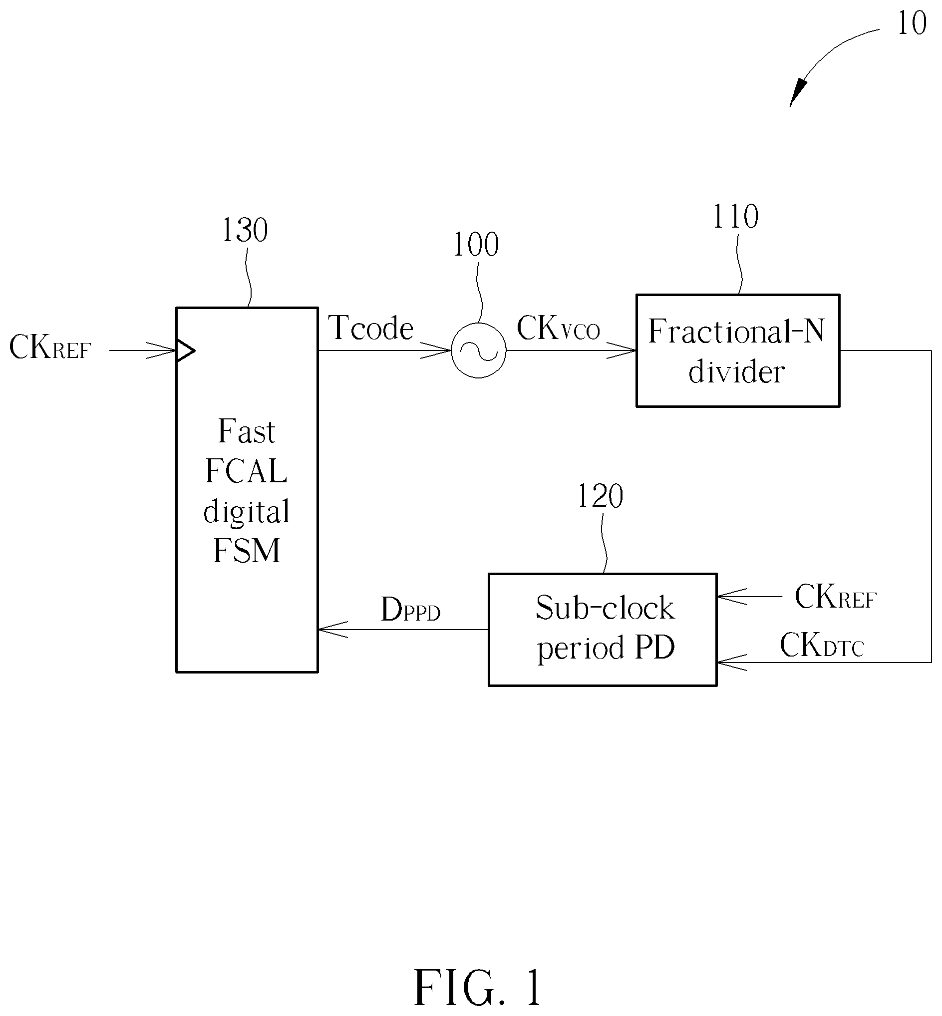
is a diagram illustrating a frequency calibration circuit according to an embodiment of the present invention.
is a diagram illustrating some signals shown in according to an embodiment of the present invention.
is a diagram illustrating detailed implementation of the frequency calibration circuit shown in according to an embodiment of the present invention.
is a diagram illustrating an example of a sub-clock period phase detector according to an embodiment of the present invention.
is a diagram illustrating operations of the sub-clock period phase detector shown in according to an embodiment of the present invention.
is a diagram illustrating a working flow of a method for calibrating an oscillation frequency of a controllable oscillator according to an embodiment of the present invention.
DETAILED DESCRIPTION
Certain terms are used throughout the following description and claims, which refer to particular components. As one skilled in the art will appreciate, electronic equipment manufacturers may refer to a component by different names. This document does not intend to distinguish between components that differ in name but not in function. In the following description and in the claims, the terms “include” and “comprise” are used in an open-ended fashion, and thus should be interpreted to mean “include, but not limited to . . . ”. Also, the term “couple” is intended to mean either an indirect or direct electrical connection. Accordingly, if one device is coupled to another device, that connection may be through a direct electrical connection, or through an indirect electrical connection via other devices and connections.
is a diagram illustrating a frequency calibration (FCAL) circuit 10 according to an embodiment of the present invention. As shown in , the FCAL circuit 10 may comprise a controllable oscillator such as a voltage controlled oscillator (VCO) 100 , a divider such as a fractional-N divider 110 , a time-to-digital converter (TDC) such as a sub-clock period phase detector (PD) 120 , and a calibration logic such as a fast FCAL digital finite state machine (FSM) 130 , where the fractional-N divider 110 is coupled to the VCO 100 , the sub-clock period PD 120 is coupled to the fractional-N divider 110 , and the fast FCAL digital FSM 130 is coupled to the VCO 100 and the sub-clock period PD 120 . In this embodiment, the VCO 100 is configured to generate a controllable oscillation clock such as a VCO clock CK VCO according to a calibration code Tcode, wherein an oscillation frequency of the VCO clock CK VCO is controlled according to the calibration code Tcode. The fractional-N divider 110 is configured to divide the oscillation frequency of the VCO clock CK VCO by a predetermined divisor to generate a divided clock CK DTC . The sub-clock period PD 120 is configured to convert a first period between a first edge of a reference clock CK REF (which may be received from a crystal oscillator) and a first edge of the divided clock CK DTC into a first period code and convert a second period between a second edge of the reference clock CK REF and a second edge of the divided clock CK DTC into a second period code. For example, the sub-clock period PD 120 may generate a period code D PPD according to the reference clock CK REF and the divided clock CK DTC , where the period code D PPD output at a first time point (e.g. at which the sub-clock period PD 120 performs a time-to-digital conversion upon the first period) may represent the first period code, and the period code D PPD output at a second time point (e.g. at which the sub-clock period PD 120 performs the time-to-digital conversion upon the second period) may represent the second period code. The fast FCAL digital FSM 130 is configured to compare the first period code and the second period code to generate a comparison result for determining whether the first period is greater or less than the second period, and control the calibration code Tcode according to the comparison result.
In this embodiment, the predetermined divisor is set according to a ratio of a target of the oscillation frequency of the VCO clock CK VCO and a reference frequency of the reference clock CK REF . For example, the predetermined divisor may be set as a calculation result of dividing the target of the oscillation frequency of the VCO clock CK VCO by the reference frequency of the reference clock CK REF . More particularly, the divider may be a divided-by-N divider such as the fractional-N divider 110 , where N may represent the predetermined divisor which is a non-integer divisor. It should be noted that the divider implemented with the fractional-N divider 110 is for illustrative purposes only, and is not meant to be a limitation of the present invention. In some embodiment, the divider may be implemented to have an integer divisor (e.g. the predetermined divisor is set to be an integer) if the target of the oscillation frequency of the VCO clock CK VCO is integer times the reference frequency of the reference clock CK REF .
is a diagram illustrating some signals such as the reference clock CK REF , the VCO clock CK REF and the divided clock CK DTC shown in according to an embodiment of the present invention. As the reference frequency of the reference clock CK REF is known and constant, a gating window specified with a certain number of cycles of the reference clock CK REF may be taken as a reference time period, and a number of cycles of the VCO clock CK VCO within the reference time period can be counted in order to determine whether the VCO clock CK VCO is too fast or too slow. A typical counter circuit is limited to obtain an integer portion of the number of cycles of the VCO clock CK VCO within the reference time period only, however. If the detection of the number of cycles of the VCO clock CK VCO within the reference time period is performed by the typical counter circuit only, a width of the gating window (i.e. a length of the reference time period) may need to be increased in order to achieve sufficient resolution of FCAL, and a total time for completing the FCAL of the oscillation frequency may be greatly increase.
In this embodiment, a starting time point (which is indicated by a first dashed line shown in ) of the gating window is specified by the first edge of the reference clock CK REF (e.g. a second rising edge of the reference clock CK REF shown in ), and an ending time point (which is indicated by a second dashed line shown in ) of the gating window is specified by the second edge of the reference clock CK REF (e.g. a sixth rising edge of the reference clock CK REF shown in ), where the first edge of the divided clock CK DTC and the second edge of the divided clock are edges (e.g. rising edges) respectively following the first edge of the reference clock CK REF and the second edge of the reference clock CK REF . For example, the first edge of the divided clock CK DTC may be a first rising edge after the starting time point of the gating window, and the second edge of the divided clock CK DTC may be a first rising edge after the ending time point of the gating window. Thus, a period T 1 shown in may be an example of the first period, and a period T 2 shown in may be an example of the second period.
As the predetermined divisor is set according to the ratio of the target of the oscillation frequency of the VCO clock CK VCO and the reference frequency of the reference clock CK REF , a divided frequency of the divided clock CK DTC is expected to be identical to the reference frequency of the reference clock CK REF when the oscillation frequency of the VCO clock CK VCO meets the target, and a time period between the first edge of the divided clock CK DTC and the second edge of the divided clock CK DTC is expected to be identical to a time period between the first edge of the reference clock CK REF and the second edge of the reference clock CK RE F. In particular, when the oscillation frequency of the VCO clock CK VCO meets the target, the When the oscillation frequency of the VCO clock CK VCO is greater than the target (i.e. the VCO clock CK VCO is too fast), the period T 2 may be less the period T 1 . When the oscillation frequency of the VCO clock CK VCO is less than the target (i.e. the VCO clock CK VCO is too slow), the period T 2 may be greater the period T 1 . Thus, the fast FCAL digital FSM 130 is configured to control the calibration code Tcode to make the second period code approach the first period code during the FCAL. For example, when the comparison result indicates that the period T 2 is less than the period T 1 , the fast FCAL digital FSM 130 may switch the calibration code Tcode to reduce the oscillation frequency of the VCO clock CK VCO . When the comparison result indicates that the period T 2 is greater than the period T 1 , the fast FCAL digital FSM 130 may switch the calibration code Tcode to increase the oscillation frequency of the VCO clock CK VCO .
is a diagram illustrating detailed implementation of the FCAL circuit 10 shown in according to an embodiment of the present invention. As shown in , the fractional-N divider 110 may comprise a divided-by-M divider 111 (labeled “/M” in for brevity), a controllable delay circuit 112 and a sigma-delta modulator (SDM) 113 , where the divided-by-M divider 111 is coupled to the VCO 100 , the controllable delay circuit 112 is coupled to the divided-by-M divider 111 , and the SDM 113 is coupled to the divided-by-M divider 111 and the controllable delay circuit 112 . In this embodiment, the divided-by-M divider 111 is configured to divide the oscillation frequency of the VCO clock CK VCO by an integer divisor to generate a divided-by-integer clock CK DIV , wherein M represents the integer divisor. The controllable delay circuit 112 may be a digital-to-time converter (DTC) or a voltage controlled delay line (VCDL), where the controllable delay circuit 112 is configured to apply a controllable delay to the divided-by-integer clock CK DIV for generating the divided clock CK DTC . More particularly, the integer divisor is controlled according to an integer portion of the predetermined divisor (e.g. an integer portion of N), and the controllable delay is controlled according to a fractional portion of the predetermined divisor (e.g. a fractional portion of N). In this embodiment, the SDM 113 is configured to generate an integer control signal IntN according to the integer portion of the predetermined divisor for controlling the integer divisor (i.e. M) and generate a fractional control signal FracN according to the fractional portion of the predetermined divisor for controlling the controllable delay. By applying the controllable delay to the divided-by-integer clock CK DIV , the divided clock CK DTC output from the controllable delay circuit 112 may be equivalent to a divided-by-N result of the VCO clock CK VCO .
In addition, the sub-clock period PD 120 may comprise multiple delay elements and multiple phase detectors such as K bang-bang phase detectors (BBPDs) PD 0 , PD 1 , PD 2 , . . . and PDK, where K may be an integer. The multiple delay elements is configured to generate multiple delayed reference clocks such as CK REF1 , CK REF2 , . . . and CK REFK by applying different delays such as T, (2×T), . . . and (K×T) to the reference clock CK REF , where T may represent a unit delay. For example, the delayed reference clock CK REF1 may have the delay of T relative to the reference clock CK REF , the delayed reference clock CK REF2 may have the delay of (2×T) relative to the reference clock CK REF , and the rest may be deduced by analogy, where the delayed reference clock CK REFK may have the delay of (K×T) relative to the reference clock CK REF .
When generating the first period code, the BBPD PD 0 is configured to detect whether the first edge of the divided clock CK DTC leads or lags with respect to a first reference edge of the reference clock CK REF (e.g. the first edge of the reference clock CK REF mentioned above) for generating a first bit of the first period code such as an output D 0 of the BBPD PD 0 at the first time point (e.g. at which the sub-clock period PD 120 performs the time-to-digital conversion upon the first period). The BBPD PD 1 is configured to detect whether the first edge of the divided clock CK DTC leads or lags with respect to a first reference edge of the reference clock CK REF1 (e.g. a delayed-by-T edge of the first edge of the reference clock CK REF ) for generating a second bit of multiple bits of the first period code such as an output D 1 of the BBPD PD 1 at the first time point. The BBPD PD 2 is configured to detect whether the first edge of the divided clock CK DTC leads or lags with respect to a first reference edge of the reference clock CK REF2 (e.g. a delayed-by-(2×T) edge of the first edge of the reference clock CK REF ) for generating a third bit of the multiple bits of the first period code such as an output D 2 of the BBPD PD 2 at the first time point. The reset may be deduced by analogy, where the BBPD PDK is configured to detect whether the first edge of the divided clock CK DTC leads or lags with respect to a first reference edge of the reference clock CK REFK (e.g. a delayed-by-(K×T) edge of the first edge of the reference clock CK REF ) for generating a (K+1) th bit of the multiple bits of the first period code such as an output DK of the BBPD PDK at the first time point.
When generating the second period code, the BBPD PD 0 is configured to detect whether the second edge of the divided clock CK DTC leads or lags with respect to a second reference edge of the reference clock CK REF (e.g. the second edge of the reference clock CK REF mentioned above) for generating a first bit of multiple bits of the second period code such as the output D 0 of the BBPD PD 0 at the second time point (e.g. at which the sub-clock period PD 120 performs the time-to-digital conversion upon the second period). The BBPD PD 1 is configured to detect whether the second edge of the divided clock CK DTC leads or lags with respect to a second reference edge of the reference clock CK REF1 (e.g. a delayed-by-T edge of the second edge of the reference clock CK REF ) for generating a second bit of the multiple bits of the second period code such as the output D 1 of the BBPD PD 1 at the second time point. The BBPD PD 2 is configured to detect whether the second edge of the divided clock CK DTC leads or lags with respect to a second reference edge of the reference clock CK REF2 (e.g. a delayed-by-(2×T) edge of the second edge of the reference clock CK REF ) for generating a third bit of the multiple bits of the second period code such as the output D 2 of the BBPD PD 2 at the second time point. The reset may be deduced by analogy, where the BBPD PDK is configured to detect whether the second edge of the divided clock CK DTC leads or lags with respect to a second reference edge of the reference clock CK REFK (e.g. a delayed-by-(K×T) edge of the second edge of the reference clock CK REF ) for generating a (K+1) th bit of the multiple bits of the second period code such as the output DK of the BBPD PDK at the second time point.
is a diagram illustrating an example of the sub-clock period phase detector 120 shown in according to an embodiment of the present invention, where takes an 11-bit architecture as an example (i.e. K=10). The multiple delay elements may comprise delay elements DL 1 , DL 2 , . . . and DL 10 , where each of the delay elements DL 1 , DL 2 , . . . and DL 10 are configured to apply a delay of 100 picoseconds (ps), that is, T=100 ps. In this embodiment, D-type flip-flops (DFFs) DFF 0 , DFF 1 , DFF 2 , . . . and DFF 10 may be examples of the multiple phase detectors mentioned above. In this embodiment, the sub-clock period phase detector 120 may further comprise AND gates 121 and 122 configured for controlling enablement of the time-to-digital conversion. For example, when an enablement control signal EN is “0”, the time-to-digital conversion may be disabled. When the enablement control signal EN is “1”, the reference clock CK REF may be output from the AND gate 121 , and the divided clock CK D IV may be output from the AND gate 122 . The enablement control signal EN may be set according to the gating window for controlling time points of performing the time-to-digital conversion upon the first period and the second period, but the present invention is not limited thereto.
In this embodiment, the delay elements DL 1 , DL 2 , . . . and DL 10 are connected in series. A signal X 0 may represent the reference clock CK REF without being delayed by any of the delay elements DL 1 , DL 2 , . . . and DL 10 , a signal X 1 may represent a delayed-by-(100 ps) signal of the reference clock CK REF (e.g. delayed by the delay element DL 1 ), a signal X 2 may represent a delayed-by-(200 ps) signal of the reference clock CK REF (e.g. delayed by the delay elements DL 1 and DL 2 ), and the reset may be deduced by analogy, where a signal X 10 may represent a delayed-by-(1000 ps) signal of the reference clock CK REF (e.g. delayed by the delay elements DL 1 , DL 2 , . . . and DL 10 ). The DFF DFF 0 may utilize a data input terminal (which is labeled “D” on the DFF DFF 0 shown in ) to receive the signal X 0 , utilize a clock input terminal (which is illustrated by a triangle on the DFF DFF 0 shown in ) to receive the divided clock CK DTC from the AND gate 122 , and utilize a data output terminal (which is labeled “Q” on the DFF DFF 0 shown in ) to generate the output D 0 . The DFF DFF 1 may utilize a data input terminal (which is labeled “D” on the DFF DFF 1 shown in ) to receive the signal X 1 , utilize a clock input terminal (which is illustrated by a triangle on the DFF DFF 1 shown in ) to receive the divided clock CK DTC from the AND gate 122 , and utilize a data output terminal (which is labeled “Q” on the DFF DFF 1 shown in ) to generate the output D 1 . The DFF DFF 2 may utilize a data input terminal (which is labeled “D” on the DFF DFF 2 shown in ) to receive the signal X 2 , utilize a clock input terminal (which is illustrated by a triangle on the DFF DFF 2 shown in ) to receive the divided clock CK DTC from the AND gate 122 , and utilize a data output terminal (which is labeled “Q” on the DFF DFF 2 shown in ) to generate the output D 2 . The rest may be deduced by analogy, where the DFF DFF 10 may utilize a data input terminal (which is labeled “D” on the DFF DFF 10 shown in ) to receive the signal X 10 , utilize a clock input terminal (which is illustrated by a triangle on the DFF DFF 10 shown in ) to receive the divided clock CK DTC from the AND gate 122 , and utilize a data output terminal (which is labeled “Q” on the DFF DFF 10 shown in ) to generate the output D 10 .
is a diagram illustrating operations of the sub-clock period phase detector 120 shown in according to an embodiment of the present invention. As shown in , the signals X 1 , X 2 , . . . and X 0 may have delayed edges of 100 ps, 200 ps, . . . and 1000 ps (labeled “100p”, “200p”, . . . and “1000p” in for brevity) relative to a reference edge (e.g. the first reference edge or the second reference edge mentioned above) of the reference clock CK REF (such as the signal X 0 ), respectively. In this embodiment, the period code D PPD may be expresses as a 11-bit signal such as {D 10 , D 9 , D 8 , D 7 , D 6 , D 5 , D 4 , D 3 , D 2 , D 1 , D 0 }. Regarding the time-to-digital conversion of the first period such as T 1 , the output D 0 may indicate whether the first period T 1 is greater than 0, the output D 1 may indicate whether the first period T 1 is greater than 100 ps, the output D 2 may indicate whether the first period T 1 is greater than 200 ps, and the rest may be deduced by analogy, where the output D 9 may indicate whether the first period T 1 is greater than 900 ps, and the output D 10 may indicate whether the first period T 1 is greater than 1000 ps. Regarding the time-to-digital conversion of the second period such as T 2 , the output D 0 may indicate whether the second period T 2 is greater than 0, the output D 1 may indicate whether the second period T 2 is greater than 100 ps, the output D 2 may indicate whether the second period T 2 is greater than 200 ps, and the rest may be deduced by analogy, where the output D 9 may indicate whether the second period T 2 is greater than 900 ps, and the output D 10 may indicate whether the second period T 2 is greater than 1000 ps.
In the embodiment of , an arrow on a row labeled “CK DTC (T 1 )” may illustrate an example of the first edge of the divided clock CK DIV , and arrows on a row labeled “CK DTC (T 2 )” may illustrate examples of the second edge of the divided clock CKDIV Different results of the second period T 2 are shown in together for better comprehension, and these results does not occurs at a same time in practice. Assume that the first period T 1 falls in an interval from 500 ps to 600 ps as show in , and the first period code such as the period code D PPD at the first time point may be {00000111111}. If the oscillation frequency of the VCO clock CK VCO is greater than the target and makes the second period T 2 be less than 500 ps (which means the VCO clock CK VCO is too fast), the second period code such as the period code D PPD at the second time point may be less than {00000111111} (labeled “DPPD<00000111111” in for better comprehension). If the oscillation frequency of the VCO clock CK VCO is less than the target and makes the second period T 2 be greater than 600 ps (which means the VCO clock CK VCO is too slow), the second period code such as the period code DPPD at the second time point may be greater than {00000111111} (labeled “DPPD>00000111111” in for better comprehension). Thus, the fast FCAL digital FSM 130 may compare the period code D PPD output at the second time point (which corresponds to the second period T 2 ) with the period code D PPD output at the first time point (which corresponds to the first period T 1 ) for determining whether the VCO clock CK VCO is too fast or too slow, and accordingly control (e.g. switch) the calibration code Tcode, in order to make the second period T 2 approach the first period T 2 (i.e. making the oscillation frequency of the VCO clock CK VCO approach the target).
is a diagram illustrating a working flow of a method for calibrating an oscillation frequency of a controllable oscillator according to an embodiment of the present invention, where the method is applicable to a FCAL circuit such as the FCAL circuit 10 shown in , and the VCO 100 may be an example of the controllable oscillator. It should be note that the working flow shown in is for illustrative purposes only, and is not meant to be a limitation of the present invention. For example, one or more steps may be added, deleted or modified in the working flow shown in . In addition, if an overall result is not changed, these steps do not have to be executed in the exact order shown in .
In Step S 610 , the FCAL circuit may utilize the controllable oscillator (e.g. the VCO 100 shown in ) to generate a controllable oscillation clock according to a calibration code, wherein the oscillation frequency of the controllable oscillation clock is controlled according to the calibration code.
In Step S 620 , the FCAL circuit may utilize a divider (e.g. the fractional-N divider 110 shown in ) to divide the oscillation frequency of the controllable oscillation clock by a predetermined divisor to generate a divided clock.
In Step S 630 , the FCAL circuit may utilize a TDC (e.g. the sub-clock period PD 120 shown in ) to convert a first period between a first edge of a reference clock and a first edge of the divided clock into a first period code and convert a second period between a second edge of the reference clock and a second edge of the divided clock into a second period code.
In Step S 640 , the FCAL circuit may utilize a calibration logic (e.g. the fast FCAL digital FSM 130 shown in ) to compare the first period code and the second period code to generate a comparison result for determining whether the first period is greater or less than the second period, and control the calibration code according to the comparison result.
It should be noted that even though the present invention performs the time-to-digital conversion upon the first period and the second period for generating the first period code and the second period code, the present invention merely needs to determine whether the second period code is greater than the first period code (e.g. whether the second period is greater than the first period) for determining whether the VCO clock CK VCO is too fast or too slow, where absolute precision of the time-to-digital conversion does not affect the comparison of the first period and the second period. Thus, performance of the circuit for performing the time-to-digital conversion is not strict and is easy to be implemented (e.g. calibration of the time-to-digital conversion is not required). In addition, comparing the first period and the second period can be regarded as utilizing the information of the fractional portion of the number of cycles of the VCO clock CK VCO within the gating window, which greatly improve the resolution of determining whether the VCO clock CK VCO is too fast or too slow in comparison with utilizing the integer portion of the number of cycles of the VCO clock CK VCO only. More particularly, the resolution of determining whether the VCO clock CK VCO is too fast or too slow may be improved by reducing the unit delay T mentioned above without increasing the width of the gating window. Thus, the resolution of the FCAL can be greatly improved without increasing an overall time for completing the FCAL. In some embodiment, the overall time for making the oscillation frequency achieve target accuracy may be greatly reduced.
To summarize, the FCAL circuit and the method provided by the embodiments of the present invention can compare the first period and the second period for determining whether the oscillation frequency is greater or less than the target, which greatly improve an overall efficiency (e.g. speed and resolution) of the FCAL. In addition, the embodiments of the present invention will not greatly increase additional costs. Thus, the present invention can improve an overall efficiency of the FCAL without introducing any side effect or in a way that is less likely to introduce side effects.
Those skilled in the art will readily observe that numerous modifications and alterations of the device and method may be made while retaining the teachings of the invention. Accordingly, the above disclosure should be construed as limited only by the metes and bounds of the appended claims.
Figures (6)
Citations
This patent cites (3)
- US8193963
- US11646743
- US2023/0170915