Abstract
A relaxation oscillator includes a start-up circuit. During the start-up period of the relaxation oscillator, two output signals from the relaxation oscillator are controlled to be complementary signals by the start-up circuit according to a control signal. Consequently, the relaxation oscillator can be started up successfully. The relaxation oscillator can generate periodic square wave signals. Moreover, during the start-up period of the relaxation oscillator, the generation of the deadlock situation can be avoided.
Claims (12)
1. A relaxation oscillator, comprising: a voltage-controlled current circuit receiving a first supply voltage, and comprising a first current path, a second current path, a third current path and a fourth current path, wherein the first current path is coupled to a first node, the second current path is coupled to a second node, the third current path is coupled to a third node, the fourth current path is coupled to a fourth node, and a voltage at the second node is a first output signal of the relaxation oscillator; a first transistor, wherein a first drain/source terminal of the first transistor is connected with the second node, a second drain/source terminal of the first transistor is connected with a fifth node, and a gate terminal of the first transistor is connected with the first node; a second transistor, wherein a first drain/source terminal of the second transistor is connected with the third node, a second drain/source terminal of the second transistor is connected with the fifth node, and a gate terminal of the second transistor is connected with the fourth node; a third transistor, wherein a first drain/source terminal of the third transistor is connected with the first node, a second drain/source terminal of the third transistor is connected with the fifth node, and a gate terminal of the third transistor is connected with the third node; a fourth transistor, wherein a first drain/source terminal of the fourth transistor is connected with the fourth node, a second drain/source terminal of the fourth transistor is connected with the fifth node, and a gate terminal of the fourth transistor is connected with the second node; a first capacitor connected between the first node and the fifth node; a second capacitor connected between the fourth node and the fifth node, wherein the fifth node receives a second supply voltage; a latching circuit wherein a first terminal of the latching circuit is connected with the second node, a second terminal of the latching circuit is connected with the third node, and a third terminal of the latching circuit is connected with the fifth node; a combinational logic circuit receiving a control signal, and generating a first signal and a second signal; a fifth transistor, wherein a first drain/source terminal of the fifth transistor is connected with the second node, a second drain/source terminal of the fifth transistor is connected with the fifth node, and a gate terminal of the fifth transistor receives the second signal; a sixth transistor, wherein a first drain/source terminal of the sixth transistor is connected with the third node, a second drain/source terminal of the sixth transistor is connected with the fifth node, and a gate terminal of the sixth transistor receives the first signal; a seventh transistor, wherein a first drain/source terminal of the seventh transistor is connected with the first node, a second drain/source terminal of the seventh transistor is connected with the fifth node, and a gate terminal of the seventh transistor receives the second signal; and an eighth transistor, wherein a first drain/source terminal of the eighth transistor is connected with the fourth node, a second drain/source terminal of the eighth transistor is connected with the fifth node, and a gate terminal of the eighth transistor receives the second signal, wherein when the control signal is inactivated, the relaxation oscillator is not in a normal working mode, wherein when the control signal is activated, the relaxation oscillator is in the normal working mode.
Show 11 dependent claims
2. The relaxation oscillator as claimed in claim 1 , wherein a voltage at the third node is a second output signal of the relaxation oscillator.
3. The relaxation oscillator as claimed in claim 1 , wherein the combinational logic circuit comprises: a NOT gate, wherein an input terminal of the NOT gate receives the control signal, and an output terminal of the NOT gate generates the first signal; a delay element, wherein an input terminal of the delay element is connected with the output terminal of the NOT gate; and an OR gate, wherein a first input the terminal of the OR gate is connected with an output terminal of the delay element, a second input terminal of the OR gate is connected with the output terminal of the OR gate, and an output terminal of the OR gate generates the second signal.
4. The relaxation oscillator as claimed in claim 1 , wherein when the control signal is activated, the sixth transistor is turned off, and the fifth transistor, the seventh transistor and the eighth transistor are turned on, wherein after the control signal has been activated for a delay time, the fifth transistor, the sixth transistor, the seventh transistor and the eighth transistor are turned off, so that the relaxation oscillator is in the normal working mode, wherein when the control signal is inactivated, the fifth transistor, the sixth transistor, the seventh transistor and the eighth transistor are turned on, so that the relaxation oscillator is disabled.
5. The relaxation oscillator as claimed in claim 1 , wherein the first current path of the voltage-controlled current circuit is directly connected with the first node, the second current path of the voltage-controlled current circuit is directly connected with the second node, the third current path of the voltage-controlled current circuit is directly connected with the third node, and the fourth current path of the voltage-controlled current circuit is directly connected with the fourth node.
6. The relaxation oscillator as claimed in claim 1 , wherein the relaxation oscillator further comprises: a ninth transistor, wherein a first drain/source terminal of the ninth transistor is connected with the second current path, a second drain/source terminal of the ninth transistor is connected with the second node, and a gate terminal of the ninth transistor receives the second signal; a tenth transistor, wherein a first drain/source terminal of the tenth transistor is connected with the third current path, a second drain/source terminal of the tenth transistor is connected with the third node, and a gate terminal of the tenth transistor receives the first signal; an eleventh transistor, wherein a first drain/source terminal of the eleventh transistor is connected with the first current path, a second drain/source terminal of the eleventh transistor is connected with the first node, and a gate terminal of the tenth transistor receives the second signal; and a twelfth transistor, wherein a first drain/source terminal of the twelfth transistor is connected with the fourth transistor, a second drain/source terminal of the twelfth transistor is connected with the fourth node, and a gate terminal of the twelfth transistor receives the second signal.
7. The relaxation oscillator as claimed in claim 6 , wherein when the control signal is activated, the tenth transistor is turned on, and the ninth transistor, the eleventh transistor and the twelfth transistor are turned off, wherein after the control signal has been activated for a delay time, the ninth transistor, the tenth transistor, the eleventh transistor and the twelfth transistor are turned on, wherein when the control signal is inactivated, the ninth transistor, the tenth transistor, the eleventh transistor and the twelfth transistor are turned off.
8. The relaxation oscillator as claimed in claim 1 , wherein the voltage-controlled current circuit comprises: a ninth transistor, wherein a first drain/source terminal of the ninth transistor receives the first supply voltage, a second drain/source terminal of the ninth transistor is the first current path, and a gate terminal of the ninth transistor receives a bias voltage; a tenth transistor, wherein a first drain/source terminal of the tenth transistor receives the first supply voltage, a second drain/source terminal of the tenth transistor is the second current path, and a gate terminal of the tenth transistor receives the bias voltage; an eleventh transistor, wherein a first drain/source terminal of the eleventh transistor receives the first supply voltage, a second drain/source terminal of the eleventh transistor is the third current path, and a gate terminal of the tenth transistor receives the bias voltage; and a twelfth transistor, wherein a first drain/source terminal of the twelfth transistor receives the first supply voltage, a second drain/source terminal of the twelfth transistor is the fourth current path, and a gate terminal of the twelfth transistor receives the bias voltage.
9. The relaxation oscillator as claimed in claim 1 , wherein the voltage-controlled current circuit comprises: a ninth transistor, wherein a first drain/source terminal of the ninth transistor receives the first supply voltage, and a gate terminal of the ninth transistor receives a first bias voltage; a tenth transistor, wherein a first drain/source terminal of the tenth transistor receives the first supply voltage, and a gate terminal of the tenth transistor receives the first bias voltage; an eleventh transistor, wherein a first drain/source terminal of the eleventh transistor receives the first supply voltage, and a gate terminal of the eleventh transistor receives the first bias voltage; a twelfth transistor, wherein a first drain/source terminal of the twelfth transistor receives the first supply voltage, and a gate terminal of the twelfth transistor receives the first bias voltage; a thirteenth transistor, wherein a first drain/source terminal of the thirteenth transistor is connected with a second drain/source terminal of the ninth transistor, a second drain/source terminal of the thirteenth transistor is the first current path, and a gate terminal of the thirteenth transistor receives a second bias voltage; a fourteenth transistor, wherein a first drain/source terminal of the fourteenth transistor is connected with a second drain/source terminal of the tenth transistor, a second drain/source terminal of the fourteenth transistor is the second current path, and a gate terminal of the fourteenth transistor receives the second bias voltage; a fifteenth transistor, wherein a first drain/source terminal of the fifteenth transistor is connected with a second drain/source terminal of the eleventh transistor, a second drain/source terminal of the fifteenth transistor is the third current path, and a gate terminal of the fifteenth transistor receives the second bias voltage; and a sixteenth transistor, wherein a first drain/source terminal of the sixteenth transistor is connected with a second drain/source terminal of the twelfth transistor, a second drain/source terminal of the sixteenth transistor is the fourth current path, and a gate terminal of the sixteenth transistor receives the second bias voltage.
10. The relaxation oscillator as claimed in claim 1 , wherein the latching circuit comprises: a ninth transistor, wherein a first drain/source terminal of the ninth transistor is connected with the second node, a second drain/source terminal of the ninth transistor is connected with the fifth node, and a gate terminal of the ninth transistor is connected with the third node; and a tenth transistor, wherein a first drain/source terminal of the tenth transistor is connected with the third node, a second drain/source terminal of the tenth transistor is connected with the fifth node, and a gate terminal of the tenth transistor is connected with the second node.
11. The relaxation oscillator as claimed in claim 10 , wherein the latching circuit further comprises: a first resistor connected between the second node and the fifth node; and a second resistor connected between the third node and the fifth node.
12. The relaxation oscillator as claimed in claim 1 , wherein the latching circuit further comprises: a first NOT gate, wherein the first NOT gate receives the first supply voltage and the second supply voltage, an input terminal of the first NOT gate is connected with the second node, and an output terminal of the first NOT gate is connected with the third node; and a second NOT gate, wherein the second NOT gate receives the first supply voltage and the second supply voltage, an input terminal of the second NOT gate is connected with the third node, and an output terminal of the second NOT gate is connected with the second node.
Full Description
Show full text →
This application claims the benefit of Taiwan Patent Application No. 112112866, filed Apr. 6, 2023, the subject matter of which is incorporated herein by reference.
FIELD OF THE INVENTION
The present invention relates to an oscillating circuit, and more particularly to a relaxation oscillator.
BACKGROUND OF THE INVENTION
As known, a relaxation oscillator is an oscillating circuit for generating a non-sinusoidal periodic signal. For example, the non-sinusoidal periodic signal is a square wave signal or a sawtooth signal.
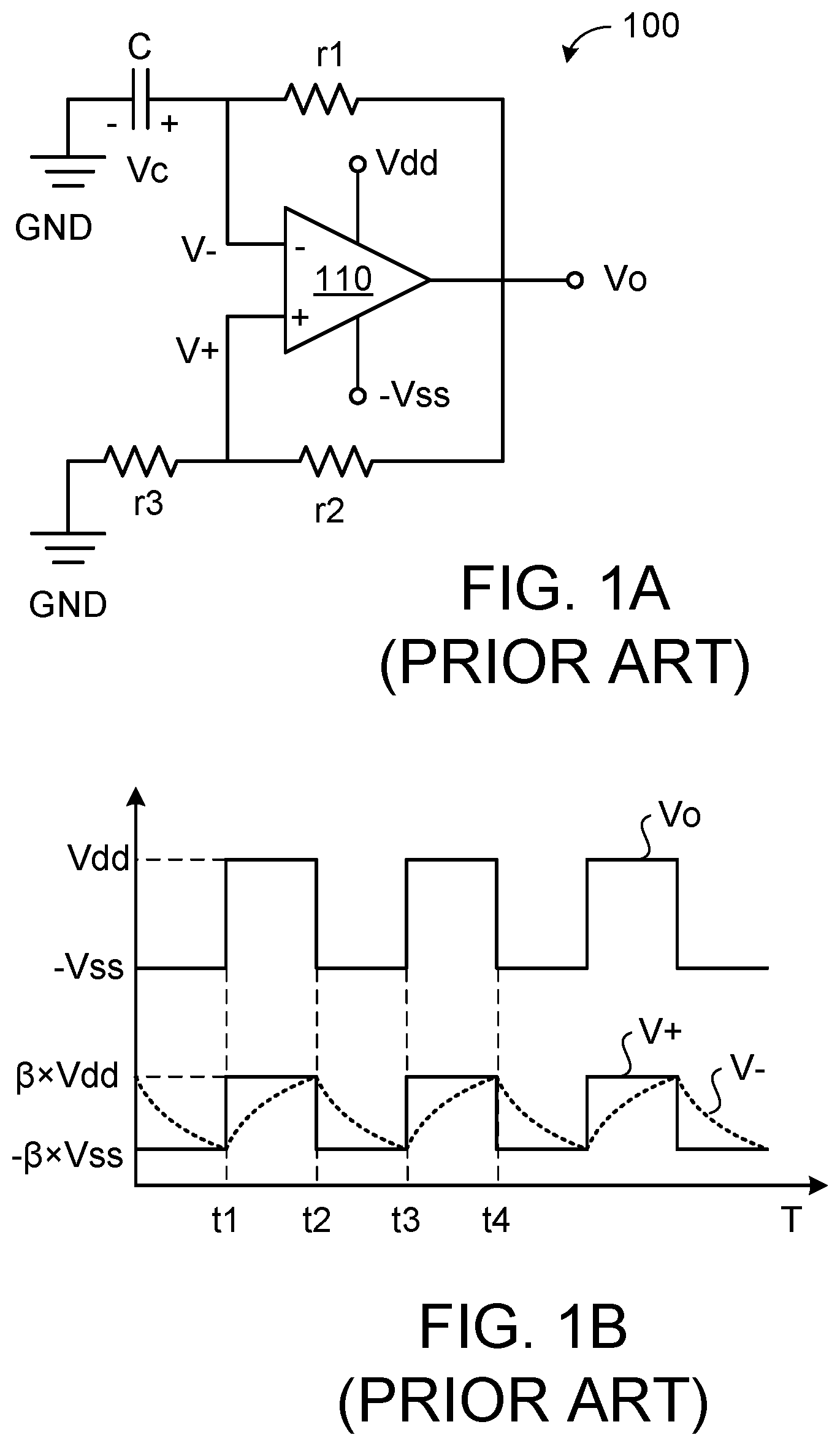
A is a schematic circuit diagram illustrating the circuitry structure of a conventional relaxation oscillator. B is a schematic timing waveform diagram illustrating associated signals of the conventional relaxation oscillator.
The relaxation oscillator 100 comprises an operational amplifier 110 , a capacitor C, and three resistors r 1 , r 2 and r 3 . The operational amplifier 110 is connected with two voltage sources. Consequently, the operational amplifier 110 receives a first supply voltage Vdd and a second supply voltage −Vss from the two voltage sources, respectively. The first supply voltage Vdd is a positive voltage. The second supply voltage −Vss is a negative voltage.
The resistor r 1 is connected between a negative input terminal of the operational amplifier 110 and an output terminal of the operational amplifier 110 . The capacitor C is connected between the negative input terminal of the operational amplifier 110 and a ground terminal GND. The resistor r 2 is connected between a positive input terminal of the operational amplifier 110 and the output terminal of the operational amplifier 110 . The resistor r 3 is connected between the positive input terminal of the operational amplifier 110 and the ground terminal GND. The voltage at the negative input terminal of the operational amplifier 110 is V−. The voltage at the positive input terminal of the operational amplifier 110 is V+. The voltage at the output terminal of the operational amplifier 110 is Vo. The voltage Vc of the capacitor C is equal to the voltage at the negative input terminal of the operational amplifier 110 . That is Vc=V−.
Please refer to A and 1 B . The resistor r 2 and the resistor r 3 are collaboratively formed as a voltage divider. It is assumed that [r 3 /(r 2 +r 3 )]=β, wherein β is greater than zero, and β is less than 1. Consequently, the relationship between the voltage V+ at the positive input terminal of the operational amplifier 110 and the voltage Vo at the output terminal of the operational amplifier 110 may be expressed as: V+=β×Vo. Consequently, if the voltage Vo at the output terminal is the first supply voltage Vdd, the voltage V+ at the positive input terminal of the operational amplifier 110 may be expressed as V+=β×Vdd. Moreover, if the voltage Vo at the output terminal of the operational amplifier 110 is the second supply voltage −Vss, the voltage V+ at the positive input terminal of the operational amplifier 110 may be expressed as V+=−β×Vss.
Please refer to B . At the time point t 1 , the voltage V− at the negative input terminal of the operational amplifier 110 is lower than the voltage V+ at the positive input terminal of the operational amplifier 110 . In addition, the voltage Vo at the output terminal of the operational amplifier 110 is switched from the second supply voltage −Vss to the first supply voltage Vdd, and the voltage V+ at the positive input terminal of the operational amplifier 110 is switched to (β×Vdd). Meanwhile, the capacitor C starts to be charged from (−β×Vss).
At the time point t 2 , the capacitor C is charged to (β×Vdd). Consequently, the voltage V− at the negative input terminal of the operational amplifier 110 is higher than the voltage V+ at the positive input terminal of the operational amplifier 110 . In addition, the voltage Vo at the output terminal of the operational amplifier 110 is switched from the first supply voltage Vdd to the second supply voltage −Vss, and the voltage V+ at the positive input terminal of the operational amplifier 110 is switched to (−β×Vss). Meanwhile, the capacitor C starts to be discharged from (β×Vdd).
Similarly, at the time point t 3 , the voltage Vo at the output terminal of the operational amplifier 110 is switched from the second supply voltage −Vss to the first supply voltage Vdd. Meanwhile, the capacitor C starts to be charged from (−β×Vss).
Similarly, at the time point t 4 , the voltage Vo at the output terminal of the operational amplifier 110 is switched from the first supply voltage Vdd to the second supply voltage −Vss. Meanwhile, the capacitor C starts to be discharged from (β×Vdd).
The rest may be deduced by analogy. The voltage Vo at the output terminal of the operational amplifier 110 is alternately switched between the first supply voltage Vdd and the second supply voltage −Vss. Consequently, in the relaxation oscillator 100 , the output terminal of the operational amplifier 110 can generate a periodic square wave signal.
SUMMARY OF THE INVENTION
An embodiment of the present invention provides a relaxation oscillator. The relaxation oscillator includes a voltage-controlled current circuit, a first transistor, a second transistor, a third transistor, a fourth transistor, a first capacitor, a second capacitor, a latching circuit, a combinational logic circuit, a fifth transistor, a sixth transistor, a seventh transistor and an eighth transistor. The voltage-controlled current circuit receives a first supply voltage. The voltage-controlled current circuit includes a first current path, a second current path, a third current path and a fourth current path. The first current path is coupled to a first node. The second current path is coupled to a second node. The third current path is coupled to a third node. The fourth current path is coupled to a fourth node. A voltage at the second node is a first output signal of the relaxation oscillator. A first drain/source terminal of the first transistor is connected with the second node. A second drain/source terminal of the first transistor is connected with a fifth node. A gate terminal of the first transistor is connected with the first node. A first drain/source terminal of the second transistor is connected with the third node. A second drain/source terminal of the second transistor is connected with the fifth node. A gate terminal of the second transistor is connected with the fourth node. A first drain/source terminal of the third transistor is connected with the first node. A second drain/source terminal of the third transistor is connected with the fifth node. A gate terminal of the third transistor is connected with the third node. A first drain/source terminal of the fourth transistor is connected with the fourth node. A second drain/source terminal of the fourth transistor is connected with the fifth node. A gate terminal of the fourth transistor is connected with the second node. A first capacitor is connected between the first node and the fifth node. A second capacitor is connected between the first node and the fifth node. The fifth node receives a second supply voltage. A first terminal of the latching circuit is connected with the second node. A second terminal of the latching circuit is connected with the third node. A third terminal of the latching circuit is connected with the fifth node. A combinational logic circuit receives a control signal and generates a first signal and a second signal. A first drain/source terminal of the fifth transistor is connected with the second node. A second drain/source terminal of the fifth transistor is connected with the fifth node. A gate terminal of the fifth transistor receives the second signal. A first drain/source terminal of the sixth transistor is connected with the third node. A second drain/source terminal of the sixth transistor is connected with the fifth node. A gate terminal of the sixth transistor receives the first signal. A first drain/source terminal of the seventh transistor is connected with the first node. A second drain/source terminal of the seventh transistor is connected with the fifth node. A gate terminal of the seventh transistor receives the second signal. A first drain/source terminal of the eighth transistor is connected with the fourth node. A second drain/source terminal of the eighth transistor is connected with the fifth node. A gate terminal of the eighth transistor receives the second signal. When the control signal is inactivated, the relaxation oscillator is not in the normal working mode. When the control signal is activated, the relaxation oscillator is in the normal working mode.
Numerous objects, features and advantages of the present invention will be readily apparent upon a reading of the following detailed description of embodiments of the present invention when taken in conjunction with the accompanying drawings. However, the drawings employed herein are for the purpose of descriptions and should not be regarded as limiting.
BRIEF DESCRIPTION OF THE DRAWINGS
The above objects and advantages of the present invention will become more readily apparent to those ordinarily skilled in the art after reviewing the following detailed description and accompanying drawings, in which:
A (prior art) is a schematic circuit diagram illustrating the circuitry structure of a conventional relaxation oscillator;
B (prior art) is a schematic timing waveform diagram illustrating associated signals of the conventional relaxation oscillator;
A is a schematic circuit diagram illustrating the circuitry structure of a relaxation oscillator according to a first embodiment of the present invention;
B is a schematic timing waveform diagram illustrating associated signals of the relaxation oscillator as shown in A and in a normal working mode;
C is a state diagram of the relaxation oscillator as shown in A and in a normal working mode;
is a schematic timing waveform diagram illustrating associated signals of the relaxation oscillator of the first embodiment during a start-up period;
A is a schematic circuit diagram illustrating the circuitry structure of a relaxation oscillator according to a second embodiment of the present invention;
B is a schematic timing waveform diagram illustrating associated signals of the relaxation oscillator according to the second embodiment of the present invention;
is a schematic circuit diagram illustrating the circuitry structure of a relaxation oscillator according to a third embodiment of the present invention;
is a schematic circuit diagram illustrating a variant example of the voltage-controlled current circuit in the relaxation oscillator of the present invention; and
A and 7 B are schematic circuit diagrams illustrating two examples of the latching circuit in the relaxation oscillator of the present invention.
DETAILED DESCRIPTION OF PREFERRED EMBODIMENTS
The present invention provides a relaxation oscillator with a novel circuitry structure. A is a schematic circuit diagram illustrating the circuitry structure of a relaxation oscillator according to a first embodiment of the present invention. As shown in A , the relaxation oscillator 200 comprises a voltage-controlled current circuit 210 , a latching circuit 220 , plural transistors M 1 ˜M 4 , and plural capacitors C 1 and C 2 . The transistors M 1 ˜M 4 are n-type transistors.
The voltage-controlled current circuit 210 receives a first supply voltage Vdd. For example, the first supply voltage Vdd is 5V. The voltage-controlled current circuit 210 comprises four current paths. The first current path is coupled to a node a. The second current path is coupled to a node b. The third current path is coupled to a node c. The fourth current path is coupled to a node d. In the relaxation oscillator 200 of the first embodiment, the four current paths are directly connected to the corresponding nodes. It is noted that numerous modifications and alterations may be made while retaining the teachings of the invention. For example, in some other embodiments, the four current paths are coupled to the corresponding nodes via other elements.
The first drain/source terminal of the transistor M 1 is connected with the node b. The second drain/source terminal of the transistor M 1 is connected with a node e. The gate terminal of the transistor M 1 is connected with the node a. The first drain/source terminal of the transistor M 2 is connected with the node c. The second drain/source terminal of the transistor M 2 is connected with the node e. The gate terminal of the transistor M 2 is connected with the node d. The first drain/source terminal of the transistor M 3 is connected with the node a. The second drain/source terminal of the transistor is connected with the node e. The gate terminal of the transistor M 3 is connected with the node c. The first drain/source terminal of the transistor M 4 is connected with the node d. The second drain/source terminal of the transistor M 4 is connected with the node e. The gate terminal of the transistor M 4 is connected with the node b.
In this embodiment, the voltage at the node b is used as a first output signal Out 1 of the relaxation oscillator 200 , and the voltage at the node c is used as a second output signal Out 2 of the relaxation oscillator 200 . It is noted that numerous modifications and alterations may be made while retaining the teachings of the invention. For example, in some other embodiments, the relaxation oscillator 200 has a single output signal only. That is, the voltage at the node b or the voltage at the node c is used as the output signal.
The capacitor C 1 is connected between the node a and the node e. The voltage difference between the node a and the node e is the voltage Vc 1 of the capacitor C 1 . The capacitor C 2 is connected between the node d and the node e. The voltage difference between the node d and the node e is the voltage Vc 2 of the capacitor C 2 . Moreover, the node e receives the second supply voltage Vss. For example, the second supply voltage Vss is a ground voltage (0V).
The voltage-controlled current circuit 210 comprises plural transistors Ma˜Md. In addition, the transistors Ma˜Md are p-type transistors. The first drain/source terminal of the transistor Ma receives the first supply voltage Vdd. The second drain/source terminal of the transistor Ma is connected with the first current path. The gate terminal of the transistor Ma receives a bias voltage Vbias. The first drain/source terminal of the transistor Mb receives the first supply voltage Vdd. The second drain/source terminal of the transistor Mb is connected with the second current path. The gate terminal of the transistor Mb receives the bias voltage Vbias. The first drain/source terminal of the transistor Mc receives the first supply voltage Vdd. The second drain/source terminal of the transistor Mc is connected with the third current path. The gate terminal of the transistor Mc receives the bias voltage Vbias. The first drain/source terminal of the transistor Md receives the first supply voltage Vdd. The second drain/source terminal of the transistor Md is connected with the fourth current path. The gate terminal of the transistor Md receives the bias voltage Vbias.
According to the bias voltage Vbias, the magnitudes of the currents outputted from the four current paths can be adjusted by the voltage-controlled current circuit 210 . In addition, the magnitudes of the currents outputted from the four current paths are in proportion to the sizes of the corresponding transistors M 1 ˜M 4 , respectively. For example, the transistors Ma˜Md have the same size. In case that the current Ia is outputted from the first output path according to the bias voltage Vbias, the magnitude of each of the currents outputted from the second, third and fourth current path is equal to the magnitude of the current Ia.
The latching circuit 220 comprises two transistors Mx and My. The transistors Mx and My are n-type transistors. The first drain/source terminal of the transistor Mx is connected with the node b. The second drain/source terminal of the transistor Mx is connected with the node e. The gate terminal of the transistor Mx is connected with the node c. The first drain/source terminal of the transistor My is connected with the node c. The second drain/source terminal of the transistor My is connected with the node e. The gate terminal of the transistor My is connected with the node b.
In case that the first output signal Out 1 is in a high voltage level state Hi and the second output signal Out 2 is in a low voltage level state Lo, it is regarded that the latching circuit 220 is in a first state. Whereas, in case that the first output signal Ou 1 is in the low voltage level state Lo and the second output signal Out 2 is in the high voltage level state Hi, it is regarded that the latching circuit 220 is in a second state. For example, the voltage level in the high voltage level state Hi is the first supply voltage Vdd, and the voltage level in the low voltage level state Lo is the second supply voltage Vss.
B is a schematic timing waveform diagram illustrating associated signals of the relaxation oscillator as shown in A and in a normal working mode.
At the time point t 1 , the voltage Vc 2 of the capacitor C 2 is charged to V th2 , wherein V th2 is a threshold voltage of the transistor M 2 . Consequently, the transistor M 2 is turned on, the voltage at the node c (i.e., the second output signal Out 2 ) is in the low voltage level state Lo, the transistor Mx is turned off, the voltage at the node b (i.e., the first output signal Out 1 ) is in the high voltage level state Hi, and the transistor My is turned on. Meanwhile, the latching circuit 220 is switched to the first state.
In the time interval between the time point t 1 and the time point t 2 , the first output signal Out 1 is in the high voltage level state Hi. Consequently, the transistor M 4 is turned on, the capacitor C 2 starts to be discharged from Vth 2 , and the voltage Vc 2 of the capacitor C 2 starts to drop. Moreover, since the second output signal Out 2 is in the low voltage level state Lo, the transistor M 3 is turned off, the capacitor C 1 starts to be charged, and the voltage Vc 1 of the capacitor C 1 starts to rise. Meanwhile, the transistors M 1 and M 2 are turned off, and the latching circuit 220 is maintained in the first state.
At the time point t 2 , the voltage Vc 1 of the capacitor C 1 is charged to V th1 , wherein V th1 is a threshold voltage of the transistor M 1 . Consequently, the transistor M 1 is turned on, the voltage at the node b (i.e., the first output signal Out 1 ) is in the low voltage level state Lo, the transistor My is turned off, the voltage at the node c (i.e., the second output signal Out 2 ) is in the high voltage level state Hi, and the transistor Mx is turned on. Meanwhile, the latching circuit 220 is switched to the second state.
In the time interval between the time point t 2 and the time point t 3 , the first output signal Out 1 is in the low voltage level state Lo. Consequently, the transistor M 4 is turned off, the capacitor C 2 starts to be charged, and the voltage Vc 2 of the capacitor C 2 starts to rise. Moreover, since the second output signal Out 2 is in the high voltage level state Hi, the transistor M 1 is turned on, the capacitor C 1 starts to be discharged from the V th1 , and the voltage Vc 1 of the capacitor C 1 starts to drop. Meanwhile, the transistors M 1 and M 2 are turned off, and the latching circuit 220 is maintained in the second state.
Similarly, at the time point t 3 , the voltage Vc 2 of the capacitor C 2 is charged to V th2 . Consequently, the transistor M 2 is turned on, the transistor My is turned on, the voltage at the node c (i.e., the second output signal Out 2 ) is in the low voltage level state Lo, the transistor Mx is turned off, and the voltage at the node b (i.e., the first output signal Out 1 ) is in the high voltage level state Hi. Meanwhile, the latching circuit 220 is switched to the first state.
Similarly, at the time point t 4 , the voltage Vc 1 of the capacitor C 1 is charged to V th1 . Consequently, the transistor M 1 is turned on, the transistor My is turned off, the voltage at the node c (i.e., the second output signal Out 2 ) is in the high voltage level state Hi, the transistor Mx is turned on, and the voltage at the node b (i.e., the first output signal Out 1 ) is in the low voltage level state Lo. Meanwhile, the latching circuit 220 is switched to the second state. The rest may be deduced by analogy.
Consequently, the first output signal Out 1 and the second output signal Out 2 outputted from the relaxation oscillator 200 are complementary to each other. In addition, the first output signal Out 1 and the second output signal Out 2 are periodic square wave signals.
C is a state diagram of the relaxation oscillator as shown in A and in a normal working mode.
In the first state of the latching circuit 220 , the first output signal Out 1 is in the high voltage level state Hi, and the second output signal Out 2 is in the low voltage level state Lo. Then, the capacitor C 1 starts to be charged, and the capacitor C 2 starts to be discharged. Consequently, the transistors M 1 and M 2 are turned off.
When the voltage Vc 1 of the capacitor C 1 is charged to V th1 , the transistor M 1 is turned on, and the transistor M 2 is maintained in the off state. Meanwhile, the latching circuit 220 is switched to second state. In the second state, the first output signal Out 1 is in the low voltage level state Lo, and the second output signal Out 2 is in the high voltage level state Hi. Then, the capacitor C 1 starts to be discharged, and the capacitor C 2 starts to be charged. Consequently, the transistors M 1 and M 2 are turned off.
When the voltage Vc 2 of the capacitor C 2 is charged to V th2 , the transistor M 2 is turned on, and the transistor M 1 is maintained in the off state. Meanwhile, the latching circuit 220 is switched to the first state. In the first state, the first output signal Out 1 is in the high voltage level state Hi, and the second output signal Out 2 is in the low voltage level state Lo.
The rest may be deduced by analogy. Consequently, the operation state of the latching circuit 220 is switched between the first state and the second state.
The operation period T of the relaxation oscillator 200 may be determined according to the current Ia of the voltage-controlled current circuit 210 , the capacitance of the capacitor C 1 , the capacitance of the capacitor C 2 , the threshold voltage V th1 of the transistor M 1 and the threshold voltage V th2 of the transistor M 2 . For example, in case that the sizes of the transistors Ma˜Md in the voltage-controlled current circuit 210 are identical, each of the four current paths generate the current Ia.
In the time interval between the time point t 1 and the time point t 2 (i.e., T 12 ), the accumulated charges Q in the capacitor C 1 may be expressed as: Q=Ia×T 12 =c 1 ×V th1 . Consequently, T 12 =(c 1 ×V th1 )/Ia. Similarly, T 23 =(c 2 ×V th2 )/Ia. In the above formulae, c 1 is the capacitance of the capacitor C 1 , and the c 2 is the capacitance of the capacitor C 2 . Consequently, the operation period T of the relaxation oscillator 200 may be expressed as: T=T 12 +T 23 .
However, when the relaxation oscillator 200 of the first embodiment is started up, a deadlock situation may be generated. The reason why the deadlock situation is generated will be described as follows.
is a schematic timing waveform diagram illustrating associated signals of the relaxation oscillator of the first embodiment during a start-up period.
At the time point t 0 , the relaxation oscillator 200 receives electric power, and the relaxation oscillator 200 is started up. For example, the first supply voltage Vdd is 5V, and the second supply voltage Vss is the ground voltage (0V). Consequently, after the time point t 0 , the first power source Vdd gradually rises, and the second supply voltage Vss is maintained in the ground voltage (0V).
At the time point t 1 , the voltage Vc 1 of the capacitor C 1 and the voltage Vc 2 of the capacitor C 2 start to rise simultaneously. Since the voltage Vc 1 of the capacitor C 1 and the voltage Vc 2 of the capacitor C 2 are not high enough to turn on the transistors M 1 and M 2 , the first output signal Out 1 and the second output signal Out 2 may be regraded to be in the high voltage level state.
At the time point t 2 , both of the transistors M 1 and M 2 are turned on and both of the transistors Mx and My are turned off according to the voltage Vc 1 of the capacitor C 1 and the voltage Vc 2 of the capacitor C 2 . Consequently, each of the first output signal Out 1 and the second output signal Out 2 is switched to the low voltage level state. Meanwhile, the voltage Vc 1 of the capacitor C 1 and the voltage Vc 2 of the capacitor C 2 continuously rise. Under this circumstance, each of the first output signal Out 1 and the second output signal Out 2 is maintained in the low voltage level state. Since the periodic square wave signal cannot be generated, the deadlock situation of the relaxation oscillator 200 occurs.
While the relaxation oscillator 200 of the first embodiment is started up, the voltage Vc 1 of the capacitor C 1 and the voltage Vc 2 of the capacitor C 2 rise simultaneously. Consequently, the first output signal Out 1 and the second output signal Out 2 cannot be formed as the complementary periodic square wave signals. That is, during the start-up period of the relaxation oscillator 200 , the deadlock situation is possibly generated. In the deadlock situation, the relaxation oscillator 200 cannot be operated normally.
In order to avoid the generation of the deadlock situation, the relaxation oscillator needs to be modified. For example, the relaxation oscillator is additionally equipped with a start-up circuit composed of electronic components, and the start-up circuit is controlled by a control signal Ctr.
A is a schematic circuit diagram illustrating the circuitry structure of a relaxation oscillator according to a second embodiment of the present invention. In comparison with the relaxation oscillator of the first embodiment, the relaxation oscillator 400 of this embodiment further comprises a combinational logic circuit 410 and plural transistors M 5 ˜M 8 . The transistors M 5 ˜M 8 are n-type transistors. The circuitry structures of the voltage-controlled current circuit 210 and the latching circuit 220 in the relaxation oscillator 400 of this embodiment are identical to those of the first embodiment, and not redundantly described herein. The connection relationships between the transistors M 1 ˜M 4 , the capacitor C 1 , the capacitor C 2 and associated components are also identical to those of the first embodiment.
The combinational logic circuit 410 comprises a NOT gate 412 , a delay element 416 and an OR gate 418 . The input terminal of the NOT gate 412 receives the control signal Ctrl. The output terminal of the NOT gate 412 generates a first signal S 1 . That is, the control signal Ctrl and the first signal S 1 are complementary to each other. Moreover, the input terminal of the delay element 416 is connected with the output terminal of the NOT gate 412 . The two input terminals of the OR gate 418 are connected with the output terminal of the NOT gate 412 and the output terminal of the delay element 416 , respectively. The output terminal of the OR gate 418 generates a second signal S 2 .
The first drain/source terminal of the transistor M 5 is connected with the node b. The second drain/source terminal of the transistor M 5 is connected with the node e. The gate terminal of the transistor M 5 receives the second signal S 2 . The first drain/source terminal of the transistor M 6 is connected with the node c. The second drain/source terminal of the transistor M 6 is connected with the node e. The gate terminal of the transistor M 6 receives the first signal S 1 . The first drain/source terminal of the transistor M 7 is connected with the node a. The second drain/source terminal of the transistor M 7 is connected with the node e. The gate terminal of the transistor M 7 receives the second signal S 2 . The first drain/source terminal of the transistor M 8 is connected with the node d. The second drain/source terminal of the transistor M 8 is connected with the node e. The gate terminal of the transistor M 8 receives the second signal S 2 .
B is a schematic timing waveform diagram illustrating associated signals of the relaxation oscillator according to the second embodiment of the present invention.
The relationship between the control signal Ctrl, the first signal S 1 and the second signal S 2 of the combinational logic circuit 410 will be described as follows.
Before the time point tb, the control signal Ctrl is inactivated, and the control signal Ctrl is in the low voltage level state Lo. At the time point tb, the control signal Ctrl is activated. Consequently, the control signal Ctrl is switched from the low voltage level state Lo to the high voltage level state Hi, and the first signal S 1 is switched from the high voltage level state Hi to the low voltage Level state Lo.
The second signal S 2 is delayed by the delay element 416 and the OR gate 418 . After a delay time T D , i.e., at the time point tc, the second signal S 2 is switched from the high voltage level state Hi to the low voltage level state Lo.
At the time point tg, the control signal Ctrl is switched from the high voltage level state Hi to the low voltage level state Lo. In addition, both of the first signal S 1 and the second signal S 2 are switched from the low voltage level state Lo to the high voltage level state Hi.
When the control signal Ctrl is inactivated, the transistors M 5 ˜M 8 are turned on according to the first signal S 1 and the second signal S 2 . Consequently, the relaxation oscillator 400 is not in the normal working mode. When the control signal Ctrl is activated, the transistors M 5 ˜M 8 are turned off according to the first signal S 1 and the second signal S 2 . Consequently, the relaxation oscillator 400 is in the normal working mode. The operations of the combinational logic circuit 410 and the transistors M 5 ˜M 8 according to the control signal Ctrl will be described in more details as follows.
In this embodiment, the transistor M 6 is controlled by the first signal S 1 , and the transistors M 5 , M 7 and M 8 are controlled by the second signal S 2 . Consequently, at the time point tb, when the control signal Ctrl is activated, the transistor M 6 is turned off. After the delay time T D (i.e., at the time point tc), the transistors M 5 , M 7 and M 8 are turned off. That is, after the time point tc, the transistors M 5 ˜M 8 are turned off. Consequently, the normal operations of the relaxation oscillator 400 are not affected by the transistors M 5 ˜M 8 . Moreover, at the time point tg, the control signal Ctrl is inactivated, and the transistors M 5 ˜M 8 are turned on simultaneously. Consequently, the relaxation oscillator 400 is disabled.
Please refer to B again. At the time point ta, the relaxation oscillator 400 receives electric power, and the relaxation oscillator 400 is started up. Since the control signal Ctrl is inactivated, the transistors M 5 ˜M 8 are turned on. In addition, the voltage Vc 1 of the capacitor C 1 , the voltage Vc 2 of the capacitor C 2 , the first output signal Out 1 and the second output signal Out 2 are maintained in the low voltage level state Lo, and the transistors M 1 ˜M 4 are turned off. Consequently, the relaxation oscillator 400 cannot be operated normally.
At the time point tb, the control signal Ctrl is activated. Under this circumstance, the transistor M 6 is turned off. Consequently, the second output signal Out 2 is switched to the high voltage level state Hi. Since the transistors M 5 , M 7 and M 8 are still turned on, the voltage Vc 1 of the capacitor C 1 , the voltage Vc 2 of the capacitor C 2 and the first output signal Out 1 are maintained in the low voltage level state Lo.
After the delay time T D (i.e., at the time point tc), the transistors M 5 , M 7 and M 8 are turned off. Meanwhile, since the first output signal Out 1 is in the low voltage level state Lo and the second output signal Out 2 is in the high voltage level state Hi, the transistor M 4 is turned off and the transistor M 3 is turned on. Consequently, the capacitor C 2 starts to be charged, and the voltage Vc 2 of the capacitor C 2 starts to rise. The voltage Vc 1 of the capacitor C 1 is maintained in the low voltage level state.
At the time point td, the voltage Vc 2 of the capacitor C 2 is charged to V th2 . Consequently, the transistor M 2 is turned on, the voltage at the node c (i.e., the second output signal Out 2 ) is in the low voltage level state Lo, the transistor Mx is turned off, the voltage at the node b (i.e., the first output signal Out 1 ) is in the high voltage level state Hi, and the transistor My is turned on. Meanwhile, the latching circuit 220 is switched to the first state.
In the time interval between the time point td and the time point te, the first output signal Out 1 is in the high voltage level state Hi. Consequently, the transistor M 4 is turned on, the capacitor C 2 starts to be discharged from V th2 , and the voltage Vc 2 of the capacitor C 2 starts to drop. Moreover, since the second output signal Out 2 is in the low voltage level state Lo, the transistor M 3 is turned off, the capacitor C 1 starts to be charged, and the voltage Vc 1 of the capacitor C 1 starts to rise. Meanwhile, the transistors M 1 and M 2 are turned off, and the latching circuit 220 is maintained in the first state.
At the time point te, the voltage Vc 1 of the capacitor C 1 is charged to V th1 . Consequently, the transistor M 1 is turned on, the voltage at the node b (i.e., the first output signal Out 1 ) is in the low voltage level state Lo, the transistor My is turned off, the voltage at the node c (i.e., the second output signal Out 2 ) is in the high voltage level state Hi, and the transistor Mx is turned on. Meanwhile, the latching circuit 220 is switched to the second state.
In the time interval between the time point te and the time point tf, the first output signal Out 1 is in the low voltage level state Lo. Consequently, the transistor M 4 is turned off, the capacitor C 2 starts to be charged, and the voltage Vc 2 of the capacitor C 2 starts to rise. Moreover, since the second output signal Out 2 is in the high voltage level state Hi, the transistor M 1 is turned on, the capacitor C 1 starts to be discharged from the V th1 , and the voltage Vc 1 of the capacitor C 1 starts to drop. Meanwhile, the transistors M 1 and M 2 are turned off, and the latching circuit 220 is maintained in the second state.
Similarly, at the time point tf, the voltage Vc 2 of the capacitor C 2 is charged to V th2 . Consequently, the transistor M 2 is turned on, the transistor My is turned on, the voltage at the node c (i.e., the second output signal Out 2 ) is in the low voltage level state Lo, the transistor Mx is turned off, and the voltage at the node b (i.e., the first output signal Out 1 ) is in the high voltage level state Hi. Meanwhile, the latching circuit 220 is switched to the first state.
As mentioned above, in the time interval between the time point tb and the time point tc, the first output signal Out 1 is controlled to be in the low voltage level state Lo and the second output signal Out 2 is controlled to be in the high voltage level state Hi by the relaxation oscillator 400 . That is, the first output signal Out 1 and the second output signal Out 2 are complementary to each other. Consequently, after the time point tc, the relaxation oscillator 400 starts to be operated normally, and the generation of the deadlock situation is avoided.
Moreover, at the time point tg, the control signal Ctrl is inactivated, and the transistors M 5 ˜M 8 are turned on simultaneously. Consequently, the first output signal Out 1 and the second output signal Out 2 are switched to the low voltage level state Lo simultaneously. Under this circumstance, the glitch of the first output signal Out 1 or the second output signal Out 2 will not be generated.
Similarly, at the time point th, the control signal Ctrl is activated again. In the time interval between the time point th and the time point ti, the first output signal Out 1 is controlled to be in the low voltage level state Lo and the second output signal Out 2 is controlled to be in the high voltage level state Hi by the relaxation oscillator 400 . After the time point ti, the relaxation oscillator 400 starts to be operated normally.
As mentioned above, the relaxation oscillator 400 of the present invention is equipped with the combinational logic circuit 410 and the transistors M 5 ˜M 8 . The combinational logic circuit 410 and the transistors M 5 ˜M 8 are collaboratively formed as a start-up circuit. Consequently, during the start-up period of the relaxation oscillator 400 , the generation of the deadlock situation is avoided.
is a schematic circuit diagram illustrating the circuitry structure of a relaxation oscillator according to a third embodiment of the present invention. In comparison with the relaxation oscillator 400 of the second embodiment, the relaxation oscillator 500 of the third embodiment further comprises transistors M 9 ˜M 11 . The transistor M 11 is coupled to the node a through the first current path. The transistor M 9 is coupled to the node b through the second current path. The transistor M 10 is coupled to the node c through the third current path. The transistor M 12 is coupled to the node d through the fourth current path.
The first drain/source terminal of the transistor M 11 is connected with the first current path. The second drain/source terminal of the transistor M 11 is connected with the node a. The gate terminal of the transistor M 11 receives the second signal S 2 . The first drain/source terminal of the transistor M 9 is connected with the second current path. The second drain/source terminal of the transistor M 9 is connected with the node b. The gate terminal of the transistor M 11 receives the second signal S 2 . The first drain/source terminal of the transistor M 10 is connected with the third current path. The second drain/source terminal of the transistor M 10 is connected with the node c. The gate terminal of the transistor M 10 receives the first signal S 1 . The first drain/source terminal of the transistor M 12 is connected with the fourth current path. The second drain/source terminal of the transistor M 12 is connected with the node d. The gate terminal of the transistor M 12 is connected with the second signal S 2 .
The transistors M 9 ˜M 12 are p-type transistors. Consequently, when the control signal Ctrl is activated, the transistor M 10 is turned on, and the transistors M 9 , M 11 and M 12 are turned off. After the control signal Ctrl has been activated for a delay time, the transistors M 9 ˜M 12 are turned on. When the control signal Ctrl is inactivated, the transistors M 9 ˜M 12 are turned off.
That is, before the relaxation oscillator 500 is operated normally, the transistor M 11 is turned off according to the second signal S 2 . Consequently, no leakage current is generated in the first current path. The transistor M 9 is turned off according to the second signal S 2 . Consequently, no leakage current is generated in the second current path. The transistor M 10 is turned off according to the first signal S 1 . Consequently, no leakage current is generated in the third current path. The transistor M 12 is turned off according to the second signal S 2 . Consequently, no leakage current is generated in the fourth current path. Moreover, when the relaxation oscillator 500 is operated normally, the transistors M 9 ˜M 12 are turned on.
As mentioned above, the relaxation oscillator 500 of the third embodiment is additionally equipped with the transistors M 9 ˜M 12 . Consequently, the generation of the leakage current by the relaxation oscillator 500 will be avoided. The operations of the relaxation oscillator 500 of the third embodiment before the normal working mode and after the normal working mode are similar to the operations of the relaxation oscillator 400 of the second embodiment, and not redundantly described herein.
Moreover, the circuitry structures of the voltage-controlled current circuit 210 and the latching circuit 220 are not restricted. The voltage-controlled current circuit 210 and the latching circuit 220 with other circuitry structures can be applied to the relaxation oscillators 200 , 400 and 500 of the present invention.
is a schematic circuit diagram illustrating a variant example of the voltage-controlled current circuit in the relaxation oscillator of the present invention. In this embodiment, the voltage-controlled current circuit 610 comprises transistors Ma 1 ˜Md 1 and Ma 2 ˜Md 2 . The transistors Ma 1 ˜Md 1 and Ma 2 ˜Md 2 are p-type transistors.
The first drain/source terminal of the transistor Ma 1 receives a first supply voltage Vdd. The gate terminal of the transistor Ma 1 receives the first bias voltage Vbias 1 . The first drain/source terminal of the transistor Mb 1 receives the first supply voltage Vdd. The gate terminal of the transistor Mb 1 receives the first bias voltage Vbias 1 . The first drain/source terminal of the transistor Mc 1 receives the first supply voltage Vdd. The gate terminal of the transistor Mc 1 receives the first bias voltage Vbias 1 . The first drain/source terminal of the transistor Md 1 receives the first supply voltage Vdd. The gate terminal of the transistor Md 1 receives the first bias voltage Vbias 1 .
The first drain/source terminal of the transistor Ma 2 is connected with the second drain/source terminal of the transistor Ma 1 . The second drain/source terminal of the transistor Ma 2 is the first current path. The gate terminal of the transistor Ma 2 receives a second bias voltage Vbias 2 . The first drain/source terminal of the transistor Mb 2 is connected with the second drain/source terminal of the transistor Mb 1 . The second drain/source terminal of the transistor Mb 2 is the second current path. The gate terminal of the transistor Mb 2 receives the second bias voltage Vbias 2 . The first drain/source terminal of the transistor Mc 2 is connected with the second drain/source terminal of the transistor Mc 1 . The second drain/source terminal of the transistor Mc 2 is the third current path. The gate terminal of the transistor Mc 2 receives the second bias voltage Vbias 2 . The first drain/source terminal of the transistor Md 2 is connected with the second drain/source terminal of the transistor Md 1 . The second drain/source terminal of the transistor Md 2 is the fourth current path. The gate terminal of the transistor Md 2 receives the second bias voltage Vbias 2 .
By providing the first bias voltage Vbias 1 and the second bias voltage Vbias 2 , the currents in the first current path, the second current path, the third current path and the fourth current path flow to the node a, the node b, the node c and the node d, respectively. In an embodiment, the first current path, the second current path, the third current path and the fourth current path are respectively and directly connected to the node a, the node b, the node c and the node d. Alternatively, in some other embodiments, the first current path, the second current path, the third current path and the fourth current path are coupled to the node a, the node b, the node c and the node d through the transistors M 9 ˜M 12 , respectively.
A and 7 B are schematic circuit diagrams illustrating two examples of the latching circuit in the relaxation oscillator of the present invention.
As shown in A , the latching circuit 710 comprises two transistors Mx and My and two resistors Rx and Ry. The first drain/source terminal of the transistor Mx is connected with the node b. The second drain/source terminal of the transistor Mx is connected with the node e. The gate terminal of the transistor Mx is connected with the node c. The first drain/source terminal of the transistor My is connected with the node c. The second drain/source terminal of the transistor My is connected with the node e. The gate terminal of the transistor My is connected with the node b. The resistor Rx is connected between the node b and the node e. The resistor Ry is connected between the node c and the node e. Since the latching circuit 710 is additionally equipped with the resistors Rx and Ry, the high voltage level and the low voltage level can be adjusted, and the operating speed of the latching circuit 710 can be increased.
As shown in B , the latching circuit 720 comprises two NOT gates 722 and 724 . The NOT gates 722 and 724 receive the first supply voltage Vdd and the second supply voltage Vss. The input terminal of the NOT gate 722 is connected with the node b. The output terminal of the NOT gate 722 is connected with the node c. The input terminal of the NOT gate 724 is connected with the node c. The output terminal of the NOT gate 724 is connected with the node b. Consequently, the voltage at the node b is the first output signal Out 1 , and the voltage at the node c is the second output signal Out 2 .
In the above embodiment, the combinational logic circuit 410 comprises the NOT gate 412 , the delay element 416 and the OR gate. The components of the combinational logic circuit are not restricted as long as the combinational logic circuit is capable of generating the signals with the signal sequence identical to that of the technology of the present invention.
From the above descriptions, the relaxation oscillator of the present invention is equipped with the combinational logic circuit. Due to the combinational logic circuit, the relaxation oscillator can be started up successfully. Consequently, during the start-up period of the relaxation oscillator, the generation of the deadlock situation can be avoided.
While the invention has been described in terms of what is presently considered to be the most practical and preferred embodiments, it is to be understood that the invention needs not be limited to the disclosed embodiment. On the contrary, it is intended to cover various modifications and similar arrangements included within the spirit and scope of the appended claims which are to be accorded with the broadest interpretation so as to encompass all such modifications and similar structures.
Figures (7)
Citations
This patent cites (4)
- US2005/0253661
- US2006/0097813
- US2014/0354364
- USWO-2009070940