Abstract
Disclosed is an RC oscillator comprising: a bias circuit, generating first and second bias currents, and outputting a charging current proportional to a total bias current that is the sum of the first and second bias currents, wherein the ratio of the first bias current to the second bias current has a positive temperature coefficient; and an oscillation circuit, for periodically charging a capacitor using the charging current output by the bias circuit, and using a voltage across a resistor through which the second bias current or a current proportional thereto flows as a reference voltage to compare with a charging voltage on the capacitor, so as to obtain a periodically oscillating clock signal. Thus, the present disclosure can compensate the positive temperature coefficient of the subsequent delay and realize the RC oscillator with low temperature drift by making the charging time of the capacitor have a negative temperature coefficient.
Claims (17)
1. An RC oscillator comprising: a bias circuit, configured to generate a first bias current and a second bias current, and output a charging current proportional to a total bias current that is the sum of the first bias current and the second bias current, wherein the ratio of the first bias current to the second bias current has a positive temperature coefficient; and an oscillation circuit, configured to periodically charge a capacitor using the charging current output by the bias circuit, and use a voltage across a resistor through which the second bias current or a current proportional thereto flows as a reference voltage to compare with a charging voltage on the capacitor, so as to obtain a periodically oscillating clock signal; wherein, the bias circuit comprises: a first bias current module, comprising a first bias resistor, a first transistor and a second transistor, and configured to generate the first bias current having a positive temperature coefficient or a current proportional to the first bias current on the first bias resistor, wherein a voltage across the first bias resistor is equal to a difference between gate-source voltages of the first transistor and the second transistor, and a second bias current module, comprising a second bias resistor and a fourth transistor, and configured to generate the second bias current having a negative temperature coefficient or a current proportional to the second bias current on the second bias resistor, wherein a voltage across the second bias resistor is equal to a gate-source voltage of the fourth transistor; wherein, the first bias current module outputs the first bias current to the second bias current module, and the second bias current module adds the first bias current and the second bias current to generate the total bias current.
Show 16 dependent claims
2. The RC oscillator according to claim 1 , wherein, the first bias current module further comprises: a first current mirror and a third transistor, wherein, the first bias resistor, the first transistor and the second transistor are coupled to the first current mirror, and the first transistor and the second transistor have a channel type opposite to that of transistors of the first current mirror, and wherein, the third transistor forms a second current mirror with a transistor in the first current mirror, the first transistor or the second transistor, wherein a third bias current is generated on the first bias resistor, and the third transistor outputs a current proportional to the third bias current as the first bias current.
3. The RC oscillator according to claim 1 , wherein, the second bias current module further comprises: a third current mirror, wherein, the second bias resistor and the fourth transistor are respectively coupled to two branches of the third current mirror, and the fourth transistor has a channel type opposite to that of transistors of the third current mirror so as to generate the second bias current on the second bias resistor.
4. The RC oscillator according to claim 3 , wherein, the first bias current module further comprises a third transistor for outputting the first bias current, wherein, the third transistor is coupled in parallel with the second bias resistor to one branch of the third current mirror, such that the fourth transistor coupled to the other branch of the third current mirror generates the total bias current.
5. The RC oscillator according to claim 1 , wherein, the first transistor and the second transistor are respectively a first NMOS transistor and a second NMOS transistor, and the fourth transistor is a fourth NMOS transistor, the first bias current module further includes: a first PMOS current mirror and a third NMOS transistor, wherein, the first bias resistor, the first NMOS transistor and the second NMOS transistor are coupled to the first PMOS current mirror, wherein a voltage across the first bias resistor is equal to a difference between gate-source voltages of the first NMOS transistor and the second NMOS transistor, and wherein, the third NMOS transistor forms a second current mirror with the first NMOS transistor or the second NMOS transistor, wherein a third bias current is generated on the first bias resistor, and the third NMOS transistor outputs a current proportional to the third bias current as the first bias current; and the second bias current module further includes: a third PMOS current mirror, wherein, the second bias resistor and the fourth NMOS transistor are respectively coupled to two branches of the third PMOS current mirror, wherein a voltage across the second bias resistor is equal to a gate-source voltage of the fourth NMOS transistor, so as to generate the second bias current on the second bias resistor, wherein, the second bias resistor and the third NMOS transistor are coupled in parallel to one branch of the third PMOS current mirror, such that the fourth NMOS transistor coupled to the other branch of the third PMOS current mirror generates the total bias current; and the bias circuit further includes a fifth PMOS transistor, for forming a fourth current mirror with a transistor in the third PMOS current mirror, and outputting the charging current proportional to the total bias current.
6. The RC oscillator according to claim 1 , wherein, the oscillation circuit comprises: a capacitor charging/discharging module, configured to use the clock signal to control on or off of a switch coupled to the capacitor, so as to alternately discharge the capacitor to the ground potential and charge the capacitor with the charging current, a comparison module, configured to compare a charging voltage on the capacitor with the reference voltage, so as to output a comparison signal as a comparison result, and a clock signal generating module, configured to shape the comparison signal into the clock signal.
7. The RC oscillator according to claim 6 , wherein, the comparison module comprises: at least one current comparator using the total bias current as a bias current.
8. The RC oscillator according to claim 5 , wherein, the oscillation circuit comprises: a capacitor charging/discharging module, configured to use the clock signal to control on or off of a switch coupled to the capacitor, so as to alternately discharge the capacitor to the ground potential and charge the capacitor with the charging current, a comparison module, configured to compare a charging voltage on the capacitor with the reference voltage, so as to output a comparison signal as a comparison result, and a clock signal generating module, configured to shape the comparison signal into the clock signal.
9. The RC oscillator according to claim 8 , wherein, the comparison module comprises a comparator, wherein the comparator uses the total bias current as a bias current such that a flipping voltage of the comparator is equal to the gate-source voltage of the fourth NMOS transistor.
10. The RC oscillator according to claim 9 , wherein, the comparator comprises: a sixth PMOS transistor, for forming a fifth current mirror with a transistor in the third PMOS current mirror, and outputting the total bias current, and a seventh NMOS transistor matched with the fourth NMOS transistor, wherein the drain of the seventh NMOS transistor is coupled to the drain of the sixth PMOS transistor, the source thereof is grounded, and the gate thereof is coupled to the drain of the fifth PMOS transistor, thereby outputting the comparison signal from the drain of the seventh NMOS transistor.
11. The RC oscillator according to claim 9 , wherein, the capacitor charging/discharging module comprises: the capacitor and a second capacitor, a first switch coupled in parallel with the capacitor and a second switch coupled between the capacitor and the drain of the fifth PMOS transistor, and a third switch coupled in parallel with the second capacitor and a fourth switch coupled between the second capacitor and the drain of the fifth PMOS transistor, wherein the first to fourth switches are respectively controlled by the clock signal or its inverted signal, such that the second switch and the third switch are turned on when the first switch and the fourth switch are turned off, and the first switch and the fourth switch are turned on when the second switch and the third switch are turned off.
12. The RC oscillator according to claim 9 , wherein, the clock signal generating module comprises: an inverter, for inverting the comparison signal, and a D flip-flop, whose data input terminal is coupled to its inverting output terminal, whose clock input terminal is coupled to an output terminal of the inverter, and whose output terminals respectively output the clock signal and its inverted signal.
13. The RC oscillator according to claim 8 , wherein, the comparison module comprises: a first comparator and a second comparator, wherein both the first comparator and the second comparator use the total bias current as a bias current, such that flipping voltages of the first comparator and the second comparator are equal to the gate-source voltage of the fourth NMOS transistor.
14. The RC oscillator according to claim 13 , wherein, the first comparator includes: a sixth PMOS transistor, for forming a fifth current mirror with a transistor in the third PMOS current mirror, and outputting the total bias current, and a seventh NMOS transistor matched with the fourth NMOS transistor, wherein the drain of the seventh NMOS transistor is coupled to the drain of the sixth PMOS transistor, the source thereof is grounded, and the gate thereof is coupled to the charging voltage on the capacitor, thereby outputting a first comparison signal from the drain of the seventh NMOS transistor, and wherein the second comparator includes: an eighth PMOS transistor, for forming a sixth current mirror with a transistor in the third PMOS current mirror, and outputting the total bias current, and a ninth NMOS transistor matched with the fourth NMOS transistor, wherein the drain of the ninth NMOS transistor is coupled to the drain of the eighth PMOS transistor, the source thereof is grounded, and the gate thereof is coupled to the charging voltage on a second capacitor, thereby outputting a second comparison signal from the drain of the ninth NMOS transistor.
15. The RC oscillator according to claim 13 , wherein, the capacitor charging/discharging module comprises: the capacitor and a second capacitor, a first switch coupled in parallel with the first capacitor and a second switch coupled between the capacitor and the drain of the fifth PMOS transistor, and a third switch coupled in parallel with the second capacitor and a fourth switch coupled between the second capacitor and the drain of the fifth PMOS transistor, wherein the first to fourth switches are respectively controlled by the clock signal or its inverted signal, such that the second switch and the third switch are turned on when the first switch and the fourth switch are turned off, and the first switch and the fourth switch are turned on when the second switch and the third switch are turned off.
16. The RC oscillator according to claim 14 , wherein, the clock signal generating module comprises: a first inverter and a second inverter, for respectively inverting the first comparison signal and the second comparison signal, and a RS flip-flop, whose input terminals are respectively coupled to the output terminals of the first inverter and the second inverter, and which outputs the clock signal and its inverted signal.
17. The RC oscillator according to claim 1 , wherein the resistance values of the first bias resistor and the second bias resistor do not vary with temperature.
Full Description
Show full text →
CROSS-REFERENCE TO RELATED APPLICATIONS
This application claims priority to Chinese patent application No. 202211709872.6 filed on Dec. 29, 2022, the disclosure of which is incorporated herein by reference in its entirety and for all purposes.
TECHNICAL FIELD
The disclosure herein relates to the field of integrated circuits, and in particular, to an RC oscillator.
BACKGROUND
On-chip RC oscillators have a wide range of applications in biomedical, MCU, wireless sensing and other fields due to their advantages of low cost, low power consumption and the like. The oscillation frequency of the existing RC oscillators is related to the delay of the internal comparator and digital logic circuit. However, the delay is greatly affected by the temperature, resulting in a large difference in frequency at different temperatures, which may affect the overall function and performance of the chip.
Therefore, an RC oscillator with low temperature drift is required.
SUMMARY
According to an aspect of the present disclosure, an RC oscillator is provided, comprising: a bias circuit, configured to generate a first bias current and a second bias current, and output a charging current proportional to a total bias current that is the sum of the first bias current and the second bias current, wherein the ratio of the first bias current to the second bias current has a positive temperature coefficient; and an oscillation circuit, configured to periodically charge a capacitor using the charging current output by the bias circuit, and use a voltage across a resistor through which the second bias current or a current proportional thereto flows as a reference voltage to compare with a charging voltage on the capacitor, so as to obtain a periodically oscillating clock signal.
BRIEF DESCRIPTION OF FIGURES
The above and other objects, features and advantages of the present disclosure will become more apparent from the more detailed description of the exemplary embodiments of the present disclosure taken in conjunction with the accompanying drawings, wherein the same reference numerals generally refer to the same parts in exemplary embodiments of the present disclosure.
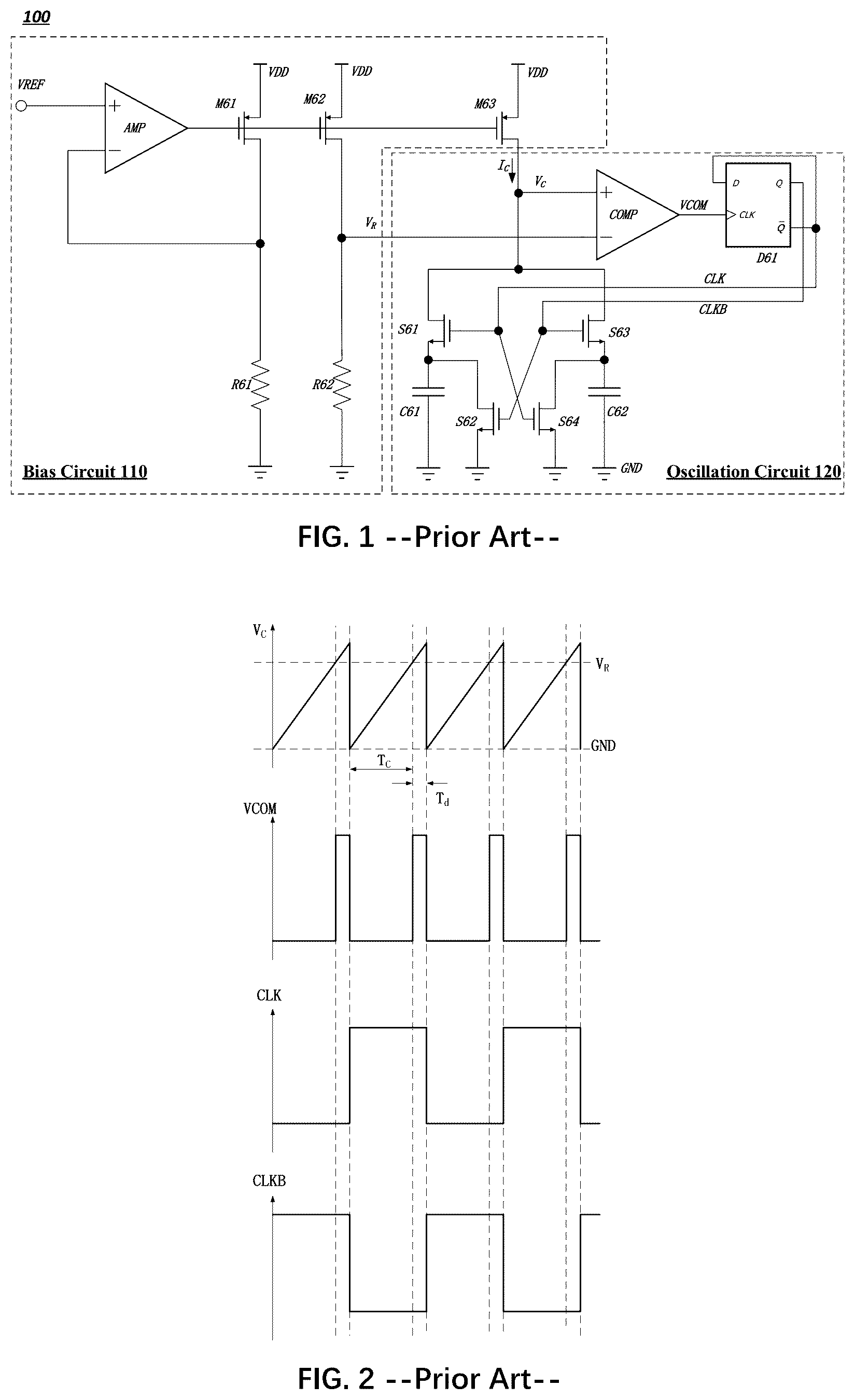
shows a schematic diagram of the composition of a typical RC oscillator.
shows some waveform examples of voltages and signals in a typical RC oscillator.
A and B respectively show schematic diagrams of the composition of an RC oscillator according to some embodiments of the present disclosure.
shows some waveform examples of voltages and signals in an RC oscillator according to an embodiment of the present disclosure.
A and B respectively show schematic diagrams of the composition of a first bias current module according to some embodiments of the present disclosure.
shows a schematic diagram of the composition of a second bias current module according to an embodiment of the present disclosure.
DETAILED DESCRIPTION
Some embodiments of the present disclosure will be described in more detail below with reference to the accompanying drawings. Although the embodiments of the present disclosure are shown in the drawings, it should be understood that the present disclosure may be embodied in various forms and should not be limited to the embodiments set forth herein. Rather, these embodiments are provided so that this disclosure will be thorough and complete, and will fully convey the scope of the disclosure to those skilled in the art.
shows a schematic diagram of the composition of a typical RC oscillator.
As shown in , the RC oscillator 100 includes a bias circuit 110 and an oscillation circuit 120 , wherein the bias circuit 110 provides the oscillation circuit 120 with a charging current I C for charging the capacitor and a reference voltage V R as a comparison reference, and the oscillation circuit 120 uses the clock signal and its inverse signal to control the periodic charging and discharging of the capacitor, compares the charging voltage on the capacitor with the reference voltage V R , and shapes the periodic oscillating signal which is the comparison result, so as to obtain the clock signal CLK with proper waveform and duty cycle.
Specifically, the bias circuit 110 includes an amplifier AMP, resistors R 61 , R 62 , and PMOS transistors M 61 , M 62 , M 63 . The operating way of the bias circuit 110 is: using the reference voltage VREF to generate a bias current=VREF/R 1 on the resistor R 61 (where R 1 is the resistance value of R 61 ), using the PMOS current mirror composed of transistors M 61 /M 62 to replicate the bias current so as to flow through the resistor R 62 , thereby generating a reference voltage V R =VREF*R 2 /R 1 (where R 2 is the resistance value of R 62 ) across the resistor R 62 , and using the PMOS current mirror consisting of transistors M 61 /M 63 to replicate the bias current as a charging current I C which is supplied to the oscillation circuit 120 . Thus I C =VREF/R 1 .
The oscillation circuit 120 includes capacitors C 61 , C 62 , switches S 61 , S 62 , S 63 , S 64 , a comparator COMP and a D flip-flop D 61 . The capacitors C 61 and C 62 have the same capacitance value C, and the switches S 61 -S 64 are all NMOS transistors. The switches S 61 and S 63 are respectively connected between the terminal of the aforementioned current mirror outputting the charging current I C and the capacitor C 61 or C 62 , and the switches S 62 and S 64 are respectively connected in parallel with the capacitor C 61 or C 62 . The clock signal CLK outputted by the D flip-flop is connected to the control terminals of the switches S 61 and S 64 , and the inverted clock signal CLKB outputted by the D flip-flop is connected to the control terminals of the switches S 62 and S 63 . Therefore, the clock signal CLK and its inverted signal CLKB can control the switches S 61 , S 64 and switches S 62 , S 63 to be turned on and off alternately, thereby controlling the capacitors C 61 and C 62 to be charged and discharged alternately. The comparator COMP compares the charging voltage V C on the capacitor C 61 or C 62 with the reference voltage V R provided by the bias circuit 110 , and outputs a comparison signal VCOM as a comparison result to the clock input terminal of the D flip-flop D 61 . The inverted output terminal Q of the D flip-flop D 61 is connected to the data input terminal D, such that the output signal CLK and its inverted signal CLKB are flipped at the rising edge of the clock input signal (i.e., the comparison signal VCOM).
shows the waveform examples of some key voltages and signals in this typical RC oscillator 100 .
The operating process of the oscillation circuit 120 will be described below with reference to and .
When the output CLK of the D flip-flop D 61 is at low level and the inverted output CLKB is at high level, the switches S 61 and S 64 are turned off, and the switches S 62 and S 63 are turned on. The capacitor C 61 is pulled down (discharged) to the ground potential GND, and the charging current I C charges the capacitor C 62 . At this time, V C is equal to the charging voltage on the capacitor C 62 , that is, the ramp signal of V C shown in , and its slope is I C /C. As shown in , the charging voltage V C on the capacitor C 62 exceeds the reference voltage V R after the time T C has elapsed. Therefore, the comparison signal VCOM outputted by the comparator COMP becomes high level, so that the output CLK of the D flip-flop D 61 and the inverted output CLKB all flip, that is, CLK becomes high level, and CLKB becomes low level. At this time, the switches S 61 and S 64 are turned on, and the switches S 62 and S 63 are turned off. V C is pulled down to the initial voltage GND of the capacitor C 61 at this time, and the charging current I C starts to charge the capacitor C 61 . The output VCOM of the comparator COMP becomes low level, and then becomes high level again when the charging voltage V C on the capacitor C 61 exceeds the reference voltage V R after the time T C passes again, and the outputs of the D flip-flop D 61 flips again, that is, CLK becomes low level, CLKB becomes high level. Then the oscillation circuit 120 repeats the above process continuously.
Please note that, as shown in , after the charging voltage V C exceeds the reference voltage V R , due to the total delay T d existing in the following comparator COMP, D flip-flop D 61 and switches S 61 -S 64 , etc., after the total delay T d , flipping all the above signals and discharging the capacitor are completed, and the charging period of the capacitor is restarted. That is, the oscillation period is 2(T C +T d ).
As shown in , T C is equal to V R divided by the slope I C /C, and as mentioned earlier, V R =VREF*R 2 /R 1 , I C =VREF/R 1 , from which T C =R 2 C can be deduced.
Therefore, the expression of the oscillation frequency (also can be said to be the clock frequency of the output clock signal) is
f = 1 2 R 2 C + 2 T d ( 1 )
It can be seen from the formula (1) that, the clock frequency is not only related to the time constant R 2 C, but also related to the total logic delay T d of the comparator, the D flip-flop and the switches. However, T d is usually very sensitive to temperature, and as the temperature rises, T d becomes larger and the clock frequency decreases. That is to say, the total logic delay T d has a positive temperature coefficient, so that the clock frequency exhibits a large temperature dependence in the entire temperature range.
In view of this, the present disclosure proposes an improved RC oscillator, which makes the charging time T C of the capacitor have a suitable negative temperature coefficient by properly setting two bias currents, thereby compensating for the positive temperature coefficient of the total logic delay T d , reducing the temperature sensitivity of the clock frequency.
Specifically, the bias circuit of the RC oscillator according to the present disclosure may generate two different bias currents (such as I a , I b described later), and output a current proportional to the sum of the two bias currents as the charging current of the capacitor in the oscillation circuit. Furthermore, the oscillation circuit according to the disclosure may use the voltage across the resistor through which one (I b ) of the two bias currents or a current proportional thereto flows, as a reference voltage for comparison with the charging voltage on the capacitor. According to the previous discussion, it can be known that, the charging time T C of the capacitor is equal to the comparison reference voltage divided by the rising slope of the charging voltage, and the slope is the ratio of the charging current to the capacitance value, thus it can be deduced that, the T C according to the present disclosure is not only related to the product of the resistance value and the capacitance value, but also is inversely proportional to the ratio (I a /I b ) of the two bias currents generated by the bias circuit (see formula (11) below). Therefore, the present disclosure compensates the positive temperature coefficient of the logic delay T d of the subsequent circuits, by setting the ratio of the two bias currents to have a positive temperature coefficient such that the charging time T C of the capacitor has a negative temperature coefficient, for example, by properly adjusting the circuit parameters so as to implement the ratio (I a /I b ) of the two bias currents to compensate for the positive temperature coefficient of T d and reduce the temperature sensitivity of the clock frequency.
Some exemplary embodiments of the present disclosure will be described below with reference to the accompanying drawings.
A and B respectively show schematic diagrams of the composition of an RC oscillator according to some embodiments of the present disclosure. As shown in A and B , the RC oscillator 300 or 300 ′ includes a bias circuit 310 and an oscillation circuit 320 or 320 ′, respectively. The difference between A and B lies in the implementation of the oscillation circuit, but the bias circuit 310 in the two is the same. The following describes the bias circuit 310 by taking A as an example.
The bias circuit 310 generates a first bias current I a and a second bias current I b , and outputs a charging current I L proportional (N times) to the total bias current I s (=I a +I b ), wherein, as will be described later in detail, I a /I b has a positive temperature coefficient.
In some embodiments, the bias circuit 310 may include a first bias current module and a second bias current module for generating two different bias currents. For example, a first bias current with a positive temperature coefficient and a second bias current with a negative temperature coefficient may be generated such that the ratio of the first bias current to the second bias current has a positive temperature coefficient.
In some embodiments, the first bias current module may use a difference between gate-source voltages of two transistors to generate a bias current on a first bias resistor. The second bias current module may use a gate-source voltage of one transistor to generate another bias current on a second bias resistor.
Another current addition module may be used to add the two bias currents to obtain the total bias current; or alternatively, as shown in A , the bias current I a generated by the first bias current module 311 may be outputted to the second bias current module 312 which also has a current addition function and adds the first bias current I a and the second bias current I b to generate the total bias current I s .
In some embodiments, the first bias current module may include: a first current mirror, as well as a first bias resistor, a first transistor and a second transistor all coupled to the first current mirror. The channel type of the first transistor and the second transistor is opposite to that of the transistors of the first current mirror, and the voltage across the first bias resistor is equal to the difference between the gate-source voltages of the first transistor and the second transistor, so as to generate a third bias current on the first bias resistor. The first bias current module may further include a third transistor, configured to form a second current mirror with the transistor in the first current mirror, the first transistor, or the second transistor, so as to output a current proportional to the third bias current as the first bias current. For example, the first current mirror or the second current mirror may be a NMOS current mirror or a PMOS current mirror. For example, the first current mirror or the second current mirror may be a cascode current mirror or other suitable current mirror.
In some embodiments, the second bias current module may include: a third current mirror, and a second bias resistor and a fourth transistor respectively coupled to two branches of the third current mirror. The channel type of the fourth transistor is opposite to that of the transistors of the third current mirror, and the voltage across the second bias resistor is equal to the gate-source voltage of the fourth transistor, thereby generating the second bias current on the second bias resistor. In addition, in some embodiments, the transistor outputting the first bias current in the first bias current module may also be coupled in parallel with the above-mentioned second bias resistor to a branch of the third current mirror such that the fourth transistor coupled to the other branch of the third current mirror generates the total bias current. That is, the second bias current module also has the function of current addition. For example, the third current mirror may be an NMOS current mirror or a PMOS current mirror. For example, the third current mirror may be a cascode current mirror or other suitable current mirror.
Certainly, those skilled in the art understand that, the bias circuit of the present disclosure is not limited to the above-mentioned bias current generation method, and the first bias current module and the second bias current module are not limited to the circuit structure shown in A , either. Rather, variations thereof are included, such as the structures shown in subsequent A- 5 B and 6 .
The operation of the bias circuit 310 according to the present disclosure will be described in detail below by taking the circuit structure of A as an example.
The first bias current module 311 includes PMOS transistors M 0 and M 1 constituting a current mirror, as well as NMOS transistors M 7 , M 9 and a bias resistor R 1 coupled to two branches of the current mirror. The sources of the NMOS transistors M 7 and M 9 are both grounded, and their gates are respectively connected to the two ends of the bias resistor R 1 . That is to say, the current I p flowing through the bias resistor R 1 is equal to the ratio of the difference between gate-source voltages of the NMOS transistors M 9 and M 7 to the resistance value R 1 of the resistor R 1 . Equal currents I p respectively flow through the two branches of the current mirror M 0 /M 1 , that is, the current I p is also the drain current of the NMOS transistors M 7 and M 9 , from which it can be deduced that:
I p = 2 μ n C ox ( W L ) 9 * 1 R S 2 ( 1 - 1 K ) 2 ( 2 )
•
• where, μ n is the electron mobility, C ox is the capacitance value of the gate oxide layer per unit area, K is the ratio of the width-to-length ratios of the transistor M 7 and the transistor M 9 , that is, K=(W/L) 7 /(W/L) 9 . μ n has a negative temperature coefficient, the capacitance value is slightly affected by temperature, and the bias resistor R 1 may be composed of two resistors with opposite temperature coefficients such that the temperature coefficient of its total resistance value R S is close to 0 (that is, the resistance value R S of the bias resistor R 1 does not change with temperature), thus the bias current I p has a positive temperature coefficient.
The first bias current module 311 also includes an NMOS transistor M 10 forming a current mirror with the transistor M 9 , which replicates the bias current I p at a certain ratio M, so as to obtain the first bias current I a as follows:
I a = 2 μ n C ox ( W L ) 9 * M R S 2 ( 1 - 1 K ) 2 ( 3 )
Since the bias current I p has a positive temperature coefficient, the first bias current I a also has a positive temperature coefficient.
As shown in A , the second bias current module 312 includes PMOS transistors M 2 and M 3 constituting a current mirror, and a bias resistor R 2 and an NMOS transistor M 11 respectively coupled to two branches of the PMOS current mirror. The source of the NMOS transistor M 11 is grounded, its gate is coupled to one end of the bias resistor R 2 , and the other end of the bias resistor R 2 is grounded. Therefore, the gate-source voltage V GS11 of the NMOS transistor M 11 is equal to the voltage across the bias resistor R 2 , in other words, the gate-source voltage of the NMOS transistor M 11 generates the following second bias current I b on the bias resistor R 2 :
I b = V GS 11 R ( 4 )
•
• where R is the resistance value of the bias resistor R 2 . Similar to the aforementioned bias resistor R 1 , the bias resistor R 2 may also be composed of two resistors with opposite temperature coefficients, such that the temperature coefficient of the resistance value R is close to 0 (that is, the resistance value R of the bias resistor R 2 does not change with temperature). Thus the temperature coefficient of I b is determined by V GS11 which usually has a negative temperature coefficient.
In combination with the foregoing, the first bias current I a has a positive temperature coefficient, and the second bias current I b has a negative temperature coefficient. Combining with the derivation of formulas (12) to (15) below, it can be known that, the ratio I a /I b of the first bias current I a to the second bias current I b also has a positive temperature coefficient.
The second bias current module 312 in A also includes an NMOS transistor M 8 , which is provided for the normal operation of the bias circuit.
In addition, the second bias current module 312 also has a current addition function, wherein the bias resistor R 2 and the transistor M 10 outputting the first bias current I a in the first bias current module 311 are coupled in parallel to a branch of the current mirror, such that the branch current of the current mirror is the total bias current I s as the sum of the two bias currents as follows:
I s = I a + I b ( 5 )
The current mirror replicates this total bias current I s to the other branch, so the drain current of transistor M 11 is also I s , thus:
I s = 1 2 μ n C ox ( W L ) 11 ( V GS 11 - V TH ) 2 ( 6 )
Wherein, (W/L) 11 is the width-to-length ratio of the transistor M 11 , and V TH is the threshold voltage of the transistor M 11 .
In addition, the bias circuit 310 also includes a PMOS transistor M 6 that forms a current mirror with the transistors in the current mirror in the second bias current module 312 , which replicates the total bias current at a certain ratio N, and thus the charging current of the capacitor is obtained as follows:
I L = N * I s ( 7 )
The oscillation circuit will be discussed below taking A and B as examples respectively.
In some embodiments, the oscillation circuit includes a capacitor charging/discharging module, a comparing module and a clock signal generating module, such as those shown in A and B .
The capacitor charging/discharging module is configured to use a clock signal to control the on-off of the switch coupled to the capacitor, so as to alternately discharge the capacitor to the ground potential and charge the capacitor with the charging current I L provided by the bias circuit. In some embodiments, the capacitor charging/discharging module 321 as shown in A (which is the same as the structure of the two capacitors S 62 and S 64 and their control switches S 61 -S 64 used in the aforementioned ), or the capacitor charging/discharging module 321 ′ as shown in B may be adopted, which both can control two symmetrical capacitors to charge and discharge alternately. Of course, those skilled in the art can understand that, only one capacitor and its control switches may be used as required, to realize the function of the capacitor charging/discharging module.
The comparison module is configured to compare the charging voltage on the capacitor in the capacitor charging/discharging module with the reference voltage provided by the bias circuit, so as to output a comparison signal as a comparison result. In some embodiments, the comparison module may include at least one current comparator, which uses the total bias current generated by the bias circuit as the bias current. For example, the comparison module 322 in A includes one current comparator, while the comparison module 322 ′ in B includes two current comparators which both use the total bias current I s as the bias current, so that the flipping voltages of these comparators both are equal to the gate-source voltage V GS11 of the NMOS transistor M 11 , that is, the voltage across the second bias resistor R 2 . In some embodiments, a voltage comparator COMP as shown in may be adopted to implement the comparison function. Of course, those skilled in the art can understand that one or two comparators can be set as required to realize the comparison function.
The clock signal generation module is configured to shape the comparison signal output by the comparison module into a clock signal. In some embodiments, the clock signal generation module 323 (including an inverter for inverting the comparison signal and a D flip-flop) as shown in A may be used to implement the shaping function to obtain a clock signal with a suitable waveform and duty cycle. In some embodiments, the clock signal generating module 323 ′ (including two inverters and a RS flip-flop) as shown in B , or the D flip-flop D 61 as shown in may be used to realize the shaping function to obtain a clock signal with a suitable waveform and duty cycle. Of course, those skilled in the art can understand that any other suitable shaping circuit can be used as required to realize the shaping function.
The operation of the oscillation circuit 320 according to the present disclosure will be described in detail below by taking the circuit structure of A as an example.
As shown in A , the oscillation circuit 320 includes a capacitor charging/discharging module 321 , a comparing module 322 and a clock signal generating module 323 .
The capacitor charging/discharging module 321 includes a first capacitor C 0 and a second capacitor C 1 , and switches M 14 -M 17 respectively coupled to the capacitors C 0 and C 1 . Capacitors C 0 and C 1 have the same capacitance value and are matched (i.e., have the same design, such as structure, size, etc.). Here the switches M 14 -M 17 are all NMOS transistors. The gate terminals of the transistors M 14 -M 17 are respectively connected to the subsequently generated non-overlapping clock signal CLK and its inverted signal CLKB, so that turning on or off of each switch is controlled by the clock signal CLK or its inverted signal CLKB. Specifically, when the clock signal CLK is at a low level, the switch M 14 coupled between the first capacitor C 0 and the drain of the transistor M 6 and the switch M 17 connected in parallel with the second capacitor C 1 are turned on, and the switch M 15 coupled between the second capacitor C 1 and the drain of the transistor M 6 and the switch M 16 connected in parallel with the first capacitor C 0 are turned off, so that the first capacitor C 0 is charged by the charging current I L and the second capacitor C 1 is discharged to ground level. On the contrary, when the clock signal CLK is at a high level, the switches M 14 and M 17 are turned off, and the switches M 15 and M 16 are turned on, so that the first capacitor C 0 is discharged to the ground level and the second capacitor C 1 is charged by the charging current I L . In fact, the capacitor charging/discharging module 321 in A has the same structure as the aforementioned two capacitors S 62 and S 64 and their control switches S 61 -S 64 used in the , whose operating process in details may refer to the previous and related descriptions.
The comparison module 322 includes a comparator (also called an inverter) composed of a PMOS transistor M 5 and an NMOS transistor M 13 . The PMOS transistor M 5 and the PMOS transistor M 2 form a current mirror, so as to output the total bias current I s as the bias current of the comparator, and the flipping voltage of the comparator is equal to the gate-source voltage V GS11 of the NMOS transistor M 11 . The NMOS transistor M 13 is matched with the NMOS transistor M 11 , its drain is coupled to the drain of the transistor M 5 , its source is grounded, and its gate is coupled to the charging voltage Vcap on the capacitor (which is also the drain of the PMOS transistor M 6 ), thereby outputting the comparison signal Vcom from the drain of the NMOS transistor M 13 .
The comparator may be regarded as a current comparator, which compares the bias current (that is, the total bias current I s ) with the drain current of the transistor M 13 . The output Vcom is high when the drain current of the transistor M 13 is less than the bias current, and the output toggles when the two are equal. The ratio of the width-to-length ratios of the PMOS transistors M 5 and M 2 are 1:1 and the two PMOS transistors are matched, and the ratio of the width-to-length ratios of the NMOS transistors M 13 and M 11 are also 1:1 and the two NMOS transistors are matched. The bias current (i.e., the total bias current I s ) is equal to the drain current of the transistor M 11 , therefore, the comparison between the drain current of the transistor M 13 and the bias current is equivalent to the comparison between the gate-source voltage (that is, the charging voltage Vcap) of the transistor M 13 and the gate-source voltage V GS11 of the transistor M 11 after the bias circuit 310 works stably. In other words, the comparator compares the gate-source voltage V GS11 (=I b *R, as mentioned above) of the transistor M 11 as a reference voltage with the charging voltage Vcap on the capacitor, thereby outputting a comparison signal Vcom.
The clock signal generation module 323 includes an inverter INV 4 and a D flip-flop. The inverter INV 4 inverts the comparison signal Vcom output by the comparison module 322 so as to invert the negative pulse of Vcom into a positive pulse. The waveform of Vcom after passing through the inverter INV 4 is the same as that of VCOM in , and the operation of the subsequent D flip-flop is also the same as that in and . Similar to , the data input terminal of the D flip-flop is coupled to its inverting output terminal, the clock input terminal of the D flip-flop is coupled to the output terminal of the inverter, and the output terminals of the D flip-flop respectively output clock signals CLK and its inverted signal CLKB.
In short, the oscillation circuit 320 of A has a structure similar to that of above, except that the voltage comparator is replaced by a current comparator and its subsequent inverter. Therefore, the operating principle and process of the oscillation circuit 320 of A is similar to that described above in conjunction with and , and will not be repeated here.
The operation of the oscillation circuit 320 ′ according to the present disclosure will be described in detail below by taking the circuit structure of B as an example.
As shown in B , the oscillation circuit 320 ′ includes a capacitor charging/discharging module 321 ′, a comparing module 322 ′ and a clock signal generating module 3231 .
The capacitor charging/discharging module 321 ′ includes a first capacitor C 0 and a second capacitor C 1 , and switches M 14 -M 17 respectively coupled to the capacitors C 0 and C 1 . Capacitors C 0 and C 1 have the same capacitance value and are matched (i.e., have the same design, such as structure, size, etc.). Here switches M 14 and M 15 are PMOS transistors, and M 16 and M 17 are NMOS transistors. The gate terminals of the transistors M 14 -M 17 are respectively connected to the subsequently generated non-overlapping clock signal CLK and its inverted signal CLKB, so that turning on or off of each switch is controlled by the clock signal CLK or its inverted signal CLKB. Specifically, when the clock signal CLK is at a high level, the switch M 14 coupled between the first capacitor C 0 and the drain of the transistor M 6 and the switch M 17 connected in parallel with the second capacitor C 1 are turned on, and the switch M 15 between the second capacitor C 1 and the drain of the transistor M 6 and the switch M 16 connected in parallel with the first capacitor C 0 are turned off, so that the first capacitor C 0 is charged by the charging current I L and the second capacitor C 1 is discharged to ground level. On the contrary, when the clock signal CLK is at a low level, the switches M 14 and M 17 are turned off, and the switches M 15 and M 16 are turned on, so that the first capacitor C 0 is discharged to the ground level and the second capacitor C 1 is charged by the charging current I L .
The comparison module 322 ′ includes a first comparator composed of a PMOS transistor M 5 and an NMOS transistor M 13 , and a second comparator composed of a PMOS transistor M 4 and an NMOS transistor M 12 . The PMOS transistors M 4 and M 5 respectively form current mirrors with the PMOS transistor M 2 , and both output the total bias current I s as the bias currents of the two comparators, so that the flipping voltages of the two comparators both are equal to the gate-source voltage V GS11 of the NMOS transistor M 11 . The NMOS transistor M 13 is matched with the NMOS transistor M 11 , its drain is coupled to the drain of the transistor M 5 , its source is grounded, and its gate is coupled to the charging voltage V 0 on the first capacitor C 0 , thereby outputting the first comparison signal V 2 from the drain of the transistor M 13 . The NMOS transistor M 12 is matched with the NMOS transistor M 11 , its drain is coupled to the drain of the transistor M 4 , its source is grounded, and its gate is coupled to the charging voltage V 1 on the second capacitor C 1 , thereby outputting the second comparison signal V 3 from the drain of the transistor M 12 .
These two comparators (also called inverters) may be regarded as current comparators, which compare the bias current (that is, the total bias current I s ) with the drain current of the transistor M 12 or M 13 . When the drain current of M 12 or M 13 is less than the bias current, the output V 3 or V 2 is at high level, and when the two are equal, the output flips. The ratio of the width-to-length ratios of the PMOS transistors M 4 , M 5 , and M 2 are 1:1:1 and these three PMOS transistors are matched, and the ratio of the width-to-length ratios of the NMOS transistors M 12 , M 13 , and M 11 are also 1:1:1 and these three NMOS transistors are matched. The bias current (that is, the total bias current I s ) is equal to the drain current of the transistor M 11 , so the comparison between the drain current of the transistor M 12 or M 13 and the bias current is equivalent to the comparison between the gate-source voltage (that is, the charging voltage V 1 or V 0 ) of the transistor M 12 or M 13 and the gate-source voltage V GS11 of the transistor M 11 after the bias circuit 310 works stably. In other words, the two comparators use the gate-source voltage V GS11 (=I b *R, as mentioned above) of the transistor M 11 as a reference voltage to compare with the charging voltage V 0 or V 1 on one of the two capacitors, thereby outputting the comparison signal V 2 or V 3 .
As mentioned above, the comparator structure in A or B is only an exemplary implementation, and the present disclosure is not limited thereto. For example, similar to the implementation in , the voltage across the bias resistor R 2 may be drawn out as the comparison reference of the voltage comparator, or alternatively, the second bias current I b or a current proportional to it may be drawn out to flow through another resistor and the voltage across the another resistor may be used as the comparison reference of the voltage comparator to compare with the charging voltage on the capacitor.
The clock signal generating module 323 includes two inverters INV 3 and INV 4 , and an RS flip-flop RS 1 . The two inverters INV 3 and INV 4 respectively invert the two comparison signals V 2 and V 3 output by the comparison module 322 so as to invert the negative pulses of V 2 and V 3 into positive pulses. The input terminals of the RS flip-flop RS 1 are respectively coupled to the output terminals of the two inverters, and the RS flip-flop RS 1 outputs the clock signal CLK and its inverted signal CLKB.
In short, the oscillation circuit 320 alternately charges and discharges the capacitors C 0 and C 1 to generate non-overlapping upward pulses at the nodes V 4 and V 5 respectively, so that the RS flip-flop RS 1 generates a pair of non-overlapping clock signals CLK and CLKB, and the clock signals CLK and CLKB are coupled to the control terminals of the switches for controlling the charging and discharging of the capacitors C 0 and C 1 , thereby controlling the charging and discharging of the capacitors.
shows an example of waveforms of some key voltages and signals in the RC oscillator 300 ′ according to an embodiment of the present disclosure.
The working process of the oscillation circuit 320 ′ will be described below with reference to B and .
After the entire RC oscillator 300 ′ is powered on, the bias circuit 310 works to generate bias currents I a , I b , I s , and output a charging current I L . At time t 0 , the outputs of the RS flip-flop RS 1 , i.e., CLK=0 and CLKB=1, so the switches M 15 and M 16 are turned on, and the switches M 14 and M 17 are turned off. The upper plate of the capacitor C 0 is grounded, and the voltage V 0 is pulled down to zero. The constant current source I L charges the capacitor C 1 linearly, and the voltage V 1 of the capacitor C 1 increases linearly. At time t 1 , the voltage V 1 increases to the flipping voltage V GS11 of the second comparator, and thus the output V 3 of the second comparator flips. After the total logic delay T d of the second comparator, the inverter INV 3 , and the RS flip-flop RS 1 , at time t 2 , the clock signal CLK is set to 1, and CLKB becomes 0. At this time, the switches M 14 and M 17 are turned on, and the switches M 15 and M 16 are turned off. The upper plate of the capacitor C 1 is grounded, and the voltage V 1 is pulled down to zero. The constant current source I L charges the capacitor C 0 linearly, and the voltage V 0 of the capacitor C 0 increases linearly. At time t 3 , the voltage V 0 increases to the flipping voltage V GS11 of the first comparator, and thus the output V 2 of the first comparator flips. After the total logic delay T d of the first comparator, the inverter INV 4 , and the RS flip-flop RS 1 , at time t 4 , the clock signal CLK is reset to 0, and CLKB becomes 1.
The above process from time t 0 to time t 4 constitutes an oscillation cycle of the oscillation circuit 320 ′, and then the circuit repeats the above process continuously. Therefore, the oscillation period T is equal to twice the sum of the charging time T C of the capacitor and the delay T d of the subsequent circuits, that is:
T = 2 ( T c + T d ) ( 8 )
The capacitor charging time from time t 0 to time t 1 is
T c = C * V GS 11 I L ( 9 )
•
• where C is the capacitance value of the capacitors C 0 and C 1 .
Combining the previous formula (9) with the previous formulas (5) and (7), the following is deduced:
T c = 1 N * CV GS 11 I a + I b ( 10 )
Combining the previous formulas (4) and (10), the following is deduced:
T c = 1 N * RC 1 + I a I b ( 11 )
As mentioned before, since the three parameters N, R, and C are little affected by temperature, the temperature coefficient of T C is negatively correlated with the temperature coefficient of the bias current ratio (I a /I b ). Since the temperature coefficient of I a /I b is positive, T C has a negative temperature coefficient, which can compensate the positive temperature coefficient of T d , thereby reducing the temperature drift of the RC oscillator.
A more detailed reasoning process for I a /I b having a positive temperature coefficient will be given below in conjunction with the previous discussion.
Combining the previous formulas (5) and (6), the following is deduced:
I a + I b = 1 2 μ n C ox ( W L ) 11 ( V GS 11 - V TH ) 2 ( 12 )
Combining the previous formulas (4) and (12), the following is deduced:
I a I b = μ n C ox ( W L ) 11 R 2 I a 1 + μ n C ox ( W L ) 11 RV TH + 1 + 2 μ n C ox ( W L ) 11 RV TH + 2 μ n C ox ( W L ) 11 R 2 I a ( 13 )
Let α=μ n C ox (W/L) 11 R 2 I a , and the following is deduced:
α = 2 M * ( W L ) 11 ( W L ) 9 * ( R R S ) 2 ( 1 - 1 K ) 2 ( 14 )
It can be known from the formula (14) that, α is the product of the ratio of the width to length ratios of the transistors and the ratio of the resistance values of the resistors, so a has nothing to do with temperature.
Combining the previous formulas (13) and (14), the following is deduced:
I a I b = α 1 + μ n C ox ( W L ) 11 RV TH + 1 + 2 μ n C ox ( W L ) 11 RV TH + 2 α ( 15 )
Since μ n and V TH have negative temperature coefficients, and the resistance value and the capacitance value are little affected by temperature as mentioned above, Ia/Ib has a positive temperature coefficient. Therefore, T C has a negative temperature coefficient as mentioned earlier. By adjusting the ratio of I a and I b properly, the positive temperature coefficient of T d can be compensated, so that the oscillation frequency exhibits low temperature drift characteristics in the entire temperature range.
A and B respectively show composition diagrams of some alternative implementations of the first bias current module 311 in A according to some embodiments of the present disclosure.
The main difference between the first bias current module 511 in A and that in A is that, the bias resistor R 1 is moved so as to be located between the source of the NMOS transistor M 7 and the ground. However, the voltage across the bias resistor R 1 is still equal to the difference between the gate-source voltages of the NMOS transistors M 9 and M 7 . The above formula (2) still applies to the bias current I p .
The main difference between the first bias current module 511 ′ of B and that in A is that, the bias resistor R 1 is moved so as to be located between the source of the PMOS transistor M 0 and the power supply voltage VDD, and the NMOS transistors M 9 and M 7 form a current mirror, replacing the PMOS current mirror. The voltage across the bias resistor R 1 is equal to the difference between the gate-source voltages of the PMOS transistors M 1 and M 0 . The bias circuit structure of B (parts except M 10 ) may be regarded as the same as that of A , wherein only the channel type of each transistor is changed. Therefore, the formula for deriving the bias current I p is similar to the above formula (2).
shows a schematic composition diagram of an alternative implementation of the second bias current module 312 in A according to an embodiment of the present disclosure.
The main difference between the second bias current module 612 in and the second bias current module 312 in A is that, an NMOS transistor M 18 is added between the source of the NMOS transistor M 11 and the ground, the gate of the NMOS transistor M 11 is connected to the gate of the NMOS transistor M 8 , the NMOS transistors M 11 and M 8 are matched (having the same width-to-length ratios), and the bias resistor R 2 is connected between the source of the NMOS transistor M 8 and the ground. Therefore, the voltage across the bias resistor R 2 is equal to the gate-source voltage V GS18 of the NMOS transistor M 18 , and the total bias current I s is the drain current of the NMOS transistor M 18 . In other words, the above-mentioned formulas may be amended by replacing V GS11 with V GS18 , so as to be applied to the circuit in .
In addition, although not shown, in some embodiments, the PMOS current mirrors in A- 3 B , A- 5 B and may have other circuit structures, such as cascode current mirrors and the like. In addition, in some embodiments, NMOS current mirrors can also be used instead of the respective PMOS current mirrors in A- 3 B , A- 5 B and . Those skilled in the art can understand that the above-mentioned circuit structures of the present disclosure can be appropriately modified as required, and these changes are all within the protection scope of the present disclosure.
Various embodiments of the present disclosure have been described above, and the foregoing descriptions are exemplary, not exhaustive, and not limiting of the disclosed embodiments. Numerous modifications and variations will be apparent to those of ordinary skill in the art without departing from the scope and spirit of the described embodiments. The terminology used herein was chosen to best explain the principles of the various embodiments, the practical application or improvement over the technology in the marketplace, or to enable others of ordinary skill in the art to understand the various embodiments disclosed herein.
While various aspects and embodiments have been disclosed herein, other aspects and embodiments will be apparent to those skilled in the art. The various aspects and embodiments disclosed herein are for purposes of illustration and are not intended to be limiting, with the true scope and spirit being indicated by the following claims.
Figures (5)
Citations
This patent cites (6)
- US6356161
- US2009/0302954
- US2013/0271231
- US2019/0149140
- US2021/0305971
- US0944169