Abstract
An electronic component includes a first and second inductor forming sections integrated with a stack, and a connection conductor layer connecting the first and second inductor forming sections inside the stack. In the first inductor forming section, two first through hole lines are connected to a wide portion of an inductor conductor layer, and two second through hole lines are connected to a narrow portion of the inductor conductor layer. In the second inductor forming section, two first through hole lines are connected to a wide portion of an inductor conductor layer, and two second through hole lines are connected to a narrow portion of the inductor conductor layer.
Claims (7)
1. A multilayer electronic component comprising: a stack including a plurality of dielectric layers stacked together; a first inductor forming section and a second inductor forming section that are integrated with the stack; and a connection conductor layer that connects the first inductor forming section and the second inductor forming section inside the stack, wherein: each of the first and second inductor forming sections includes an inductor conductor layer, a plurality of first through hole lines, and a plurality of second through hole lines; each of the first through hole lines is formed by connecting two or more first through holes in series; each of the second through hole lines is formed by connecting two or more second through holes in series; a number of first through hole lines and a number of second through hole lines are the same; in each of the first and second inductor forming sections, the plurality of first through hole lines are arranged in one direction orthogonal to a stacking direction of the dielectric layers, and the plurality of second through hole lines are arranged in another direction orthogonal to the stacking direction of the dielectric layers; the inductor conductor layer has a wide end and a narrow end located at opposite ends in a longitudinal direction of the inductor conductor layer; the inductor conductor layer includes a wide portion including the wide end and a narrow portion including the narrow end; a dimension of the narrow portion in a transverse direction of the inductor conductor layer is smaller than a dimension of the wide portion in the transverse direction of the inductor conductor layer; the wide portion of the inductor conductor layer of the first inductor forming section and the narrow portion of the inductor conductor layer of the second inductor forming section adjoin at a predetermined distance; the narrow portion of the inductor conductor layer of the first inductor forming section and the wide portion of the inductor conductor layer of the second inductor forming section adjoin at a predetermined distance; in each of the first and second inductor forming sections, the plurality of first through hole lines are connected to one of the wide and narrow portions, and the plurality of second through hole lines are connected to the other of the wide and narrow portions; and the connection conductor layer connects a plurality of portions of the plurality of second through hole lines of the first inductor forming section away from the inductor conductor layer to a plurality of portions of the plurality of second through hole lines of the second inductor forming section away from the inductor conductor layer.
Show 6 dependent claims
2. The multilayer electronic component according to claim 1 , wherein the plurality of first through hole lines are arranged in a first direction, and the plurality of second through hole lines are arranged in a second direction intersecting the first direction.
3. The multilayer electronic component according to claim 2 , wherein the first direction and the second direction are orthogonal to each other.
4. The multilayer electronic component according to claim 2 , wherein: one of the first and second directions is parallel to a longitudinal direction of the inductor conductor layer; and the other of the first and second directions is parallel to the transverse direction of the inductor conductor layer.
5. The multilayer electronic component according to claim 1 , wherein: the inductor conductor layer further includes a width changing portion interposed between the narrow portion and the wide portion; and a dimension of the width changing portion in the transverse direction of the inductor conductor layer increases as a distance of the width changing portion from the narrow portion increases.
6. The multilayer electronic component according to claim 1 , wherein the first inductor forming section, the second inductor forming section, and the connection conductor layer constitute an inductor.
7. The multilayer electronic component according to claim 6 , further comprising: a first port; a second port; and a plurality of resonators that are provided between the first port and the second port in a circuit configuration and are configured so that two adjoining resonators in the circuit configuration are electromagnetically coupled to each other, wherein: the first port, the second port, and the plurality of resonators are integrated with the stack; the plurality of resonators include a first resonator closest to the first port in the circuit configuration and a second resonator closest to the second port in the circuit configuration; and each of the first and second resonators includes the inductor.
Full Description
Show full text →
BACKGROUND OF THE INVENTION
1. Field of the Invention
The present invention relates to a multilayer electronic component including inductors.
2. Description of the Related Art
The recent market demands for reductions in size and footprint of the compact mobile communication apparatuses have also required miniaturization of band-pass filters for use in those communication apparatuses. Among known band-pass filters suited for miniaturization are ones that use a stack of dielectric layers and conductor layers.
Some band-pass filters include a plurality of resonators. The plurality of resonators are configured so that two resonators adjoining in a circuit configuration are electromagnetically coupled with each other.
US 2019/0173447 A1 discloses a multilayer LC filter including a plurality of LC resonators inside a stack. In the multilayer LC filter, each LC resonator includes an inductor composed of line-shaped conductor traces and a plurality of via conductors. Each line-shaped conductor trace is formed so that its opposite long sides are nonparallel. Two via conductors are connected to the relatively longer one of the two opposite short sides of each line-shaped conductor trace, and one via conductor is connected to the relatively shorter one.
As the inductors are reduced in size for the miniaturization of the band-pass filter, the inductances and the Q values of the inductors also decrease. The inductances of the inductors configured as disclosed in US 2019/0173447 A1 can be increased by increasing the numbers of turns of the inductors. In such a case, contrivances are desired to increase the Q values as well. However, such contrivances have not heretofore been given due consideration.
The foregoing problem is not limited to band-pass filters and applies to multilayer electronic components including inductors in general.
SUMMARY OF THE INVENTION
An object of the present invention is to provide a multilayer electronic component including an inductor that has favorable characteristics and is suited for miniaturization.
A multilayer electronic component according to the present invention includes a stack including a plurality of dielectric layers stacked together, a first inductor forming section and a second inductor forming section that are integrated with the stack, and a connection conductor layer that connects the first inductor forming section and the second inductor forming section inside the stack. Each of the first and second inductor forming sections includes an inductor conductor layer, a plurality of first through hole lines, and a plurality of second through hole lines.
Each of the first through hole lines is formed by connecting two or more first through holes in series. Each of the second through hole lines is formed by connecting two or more second through holes in series. The number of first through hole lines and the number of second through hole lines are the same. In each of the first and second inductor forming sections, the plurality of first through hole lines are arranged in one direction orthogonal to a stacking direction of the dielectric layers, and the plurality of second through hole lines are arranged in another direction orthogonal to the stacking direction of the dielectric layers.
The inductor conductor layer has a wide end and a narrow end located at opposite ends in a longitudinal direction of the inductor conductor layer. The inductor conductor layer includes a wide portion including the wide end and a narrow portion including the narrow end. A dimension of the narrow portion in a transverse direction of the inductor conductor layer is smaller than a dimension of the wide portion in the transverse direction of the inductor conductor layer. The wide portion of the inductor conductor layer of the first inductor forming section and the narrow portion of the inductor conductor layer of the second inductor forming section adjoin at a predetermined distance. The narrow portion of the inductor conductor layer of the first inductor forming section and the wide portion of the inductor conductor layer of the second inductor forming section adjoin at a predetermined distance.
In each of the first and second inductor forming sections, the plurality of first through hole lines are connected to one of the wide and narrow portions, and the plurality of second through hole lines are connected to the other of the wide and narrow portions. The connection conductor layer connects a plurality of portions of the plurality of second through hole lines of the first inductor forming section away from the inductor conductor layer to a plurality of portions of the plurality of second through hole lines of the second inductor forming section away from the inductor conductor layer.
In the multilayer electronic component according to the present invention, the plurality of first through hole lines may be arranged in a first direction, and the plurality of second through hole lines may be arranged in a second direction intersecting the first direction. In such a case, the first direction and the second direction may be orthogonal to each other. One of the first and second directions may be parallel to the longitudinal direction of the inductor conductor layer, and the other of the first and second directions may be parallel to the transverse direction of the inductor conductor layer.
In the multilayer electronic component according to the present invention, the inductor conductor layer may further include a width changing portion interposed between the narrow portion and the wide portion. In such a case, a dimension of the width changing portion in the transverse direction of the inductor conductor layer may increase as a distance of the width changing portion from the narrow portion increases.
In the multilayer electronic component according to the present invention, the first inductor forming section, the second inductor forming section, and the connection conductor layer may constitute an inductor. In such a case, the multilayer electronic component according to the present invention may further include a first port, a second port, and a plurality of resonators that are provided between the first port and the second port in a circuit configuration and are configured so that two adjoining resonators in the circuit configuration are electromagnetically coupled to each other. The first port, the second port, and the plurality of resonators may be integrated with the stack. The plurality of resonators may include a first resonator closest to the first port in the circuit configuration and a second resonator closest to the second port in the circuit configuration. Each of the first and second resonators may include the inductor.
In each of the first and second inductor forming sections of the multilayer electronic component according to the present invention, the plurality of first through hole lines are connected to one of the wide and narrow portions of the inductor conductor layer, and the plurality of second through hole lines are connected to the other of the wide and narrow portions of the inductor conductor layer. The number of first through hole lines and the number of second through hole lines are the same. According to the present invention, a multilayer electronic component including an inductor that has favorable characteristics and is suited for miniaturization can thus be implemented.
Other and further objects, features and advantages of the present invention will appear more fully from the following description.
BRIEF DESCRIPTION OF THE DRAWINGS
is a circuit diagram showing circuit configuration of a multilayer electronic component according to an embodiment of the invention.
is a perspective view showing an outside view of the multilayer electronic component according to the embodiment of the invention.
A to C are explanatory diagrams showing respective patterned surfaces of first to third dielectric layers of a stack of the multilayer electronic component according to the embodiment of the invention.
A to C are explanatory diagrams showing respective patterned surfaces of fourth to sixth dielectric layers of the stack of the multilayer electronic component according to the embodiment of the invention.
A is an explanatory diagram showing a patterned surface of a seventh dielectric layer of the stack of the multilayer electronic component according to the embodiment of the invention.
B is an explanatory diagram showing respective patterned surfaces of eighth to seventeenth dielectric layers of the stack of the multilayer electronic component according to the embodiment of the invention.
C is an explanatory diagram showing a patterned surface of an eighteenth dielectric layer of the stack of the multilayer electronic component according to the embodiment of the invention.
A to C are explanatory diagrams showing respective patterned surfaces of nineteenth to twenty-first dielectric layers of the stack of the multilayer electronic component according to the embodiment of the invention.
is a perspective view showing an internal structure of the stack of the multilayer electronic component according to the embodiment of the invention.
is a plan view showing a part of the internal structure of the stack shown in .
is a characteristic chart showing an example of a pass characteristic of the multilayer electronic component according to the embodiment of the present invention.
is a characteristic chart showing an example of a reflection characteristic at a first port of the multilayer electronic component according to the embodiment of the present invention.
is a characteristic chart showing an example of a reflection characteristic at a second port of the multilayer electronic component according to the embodiment of the present invention.
DETAILED DESCRIPTION OF THE PREFERRED EMBODIMENTS
An embodiment of the present invention will now be described in detail with reference to the drawings. First, a configuration of a multilayer electronic component (hereinafter simply referred to as electronic component) according to the embodiment of the invention will be outlined with reference to . The electronic component 1 according to the present embodiment includes at least an inductor. In , a band-pass filter is shown as an example of the electronic component 1 including an inductor.
The electronic component 1 includes a first port 2 , a second port 3 , and a plurality of resonators provided between the first port 2 and the second port 3 in circuit configuration. The plurality of resonators are configured so that two adjoining resonators in the circuit configuration are electromagnetically coupled with each other. Each of the resonators includes an inductor.
In the present embodiment, the plurality of resonators are four resonators 11 , 12 , 13 , and 14 . The resonator 11 is the closest to the first port 2 in the circuit configuration. The resonator 14 is the closest to the second port 3 in the circuit configuration. The resonators 12 and 13 are located between the resonator 11 and the resonator 14 in the circuit configuration. In the present application, the expression of “in a (the) circuit configuration” is used not to indicate layout in physical configuration but to indicate layout in the circuit diagram.
The resonator 11 corresponds to “the first resonator” in the present invention. The resonator 14 corresponds to “the second resonator” in the present invention.
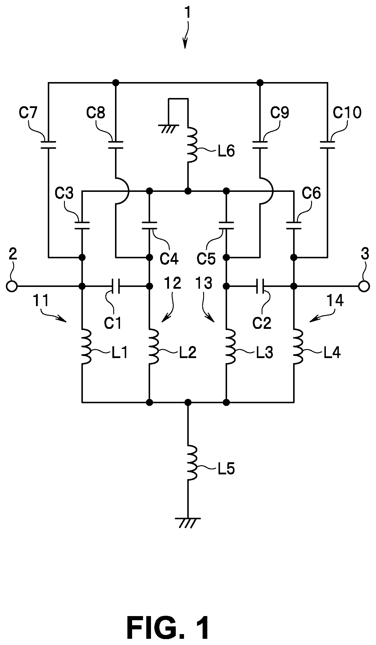
An example of the circuit configuration of the electronic component 1 including the band-pass filter will be described below with reference to . shows the components of the band-pass filter included in the electronic component 1 . The electronic component 1 further includes inductors L 1 , L 2 , L 3 , L 4 , L 5 , and L 6 , and capacitors C 1 , C 2 , C 3 , C 4 , C 5 , C 6 , C 7 , C 8 , C 9 , and C 10 .
One end of the inductor L 1 is connected to the first port 2 . The capacitor C 1 connects the one end of the inductor L 1 and one end of the inductor L 2 . One end of the inductor L 4 is connected to the second port 3 . The capacitor C 2 connects one end of the inductor L 3 and the one end of the inductor L 4 . The inductor L 5 connects the other ends of the respective inductors L 1 to L 4 to a ground.
One end of each of the capacitors C 3 and C 7 is connected to the one end of the inductor L 1 . One end of each of the capacitors C 4 and C 8 is connected to the one end of the inductor L 2 . One end of each of the capacitors C 5 and C 9 is connected to the one end of the inductor L 3 . One end of each of the capacitors C 6 and C 10 is connected to the one end of the inductor L 4 . The inductor L 6 connects the other ends of the respective capacitors C 3 to C 6 to the ground. The other ends of the respective capacitors C 7 to C 10 are connected to each other.
The resonator 11 includes the inductor L 1 . The resonator 12 includes the inductor L 2 . The resonator 13 includes the inductor L 3 . The resonator 14 includes the inductor L 4 .
Next, other configurations of the electronic component 1 will be described with reference to . is a perspective view showing an outside view of the electronic component 1 .
The electronic component 1 further includes a stack 50 including a plurality of dielectric layers stacked together. The components of the band-pass filter shown in are integrated with the stack 50 . As will be described below, the components of the band-pass filter are formed using a plurality of conductors formed in the stack 50 .
The stack 50 has a bottom surface 50 A and a top surface 50 B located at both ends in a stacking direction T of the plurality of dielectric layers, and four side surfaces 50 C to 50 F connecting the bottom surface 50 A and the top surface 50 B. The side surfaces 50 C and 50 D are opposite to each other. The side surfaces 50 E and 50 F are opposite to each other. The side surfaces 50 C to 50 F are perpendicular to the top surface 50 B and the bottom surface 50 A.
Here, X, Y, and Z directions are defined as shown in . The X, Y, and Z directions are orthogonal to one another. In the present embodiment, a direction parallel to the stacking direction T will be referred to as the Z direction. The opposite directions to the X, Y, and Z directions are defined as —X, —Y, and —Z directions, respectively.
As shown in , the bottom surface 50 A is located at the end of the stack 50 in the —Z direction. The top surface 50 B is located at the end of the stack 50 in the Z direction. The bottom surface 50 A and the top surface 50 B each have a rectangular shape long in the X direction. The side surface 50 C is located at the end of the stack 50 in the —X direction. The side surface 50 D is located at the end of the stack 50 in the X direction. The side surface 50 E is located at the end of the stack 50 in the —Y direction. The side surface 50 F is located at the end of the stack 50 in the Y direction.
The electronic component 1 further includes a plurality of terminals 111 , 112 , and 113 located at the bottom surface 50 A of the stack 50 . The terminal 111 extends in the Y direction near the side surface 50 C. The terminal 112 extends in the Y direction near the side surface 50 D. The terminal 113 is located between the terminal 111 and the terminal 112 .
The terminal 111 corresponds to the first port 2 . The terminal 112 corresponds to the second port 3 . The first and second ports 2 and 3 are thus located at the bottom surface 50 A of the stack 50 . The terminal 113 is connected to the ground.
Next, an example of the plurality of dielectric layers constituting the stack 50 will be described with reference to A to C . In this example, the stack 50 includes twenty-one dielectric layers stacked together. The twenty-one dielectric layers will be referred to as a first to a twenty-first dielectric layer in the order from bottom to top. The first to twenty-first dielectric layers are denoted by reference numerals 51 to 71 , respectively.
A shows the patterned surface of the first dielectric layer 51 . The terminals 111 , 112 , and 113 are formed on the patterned surface of the dielectric layer 51 . Further, two through holes 51 T 1 , three through holes 51 T 2 , though holes 51 T 3 and 51 T 4 , and two through holes 51 T 11 are formed in the dielectric layer 51 . The through holes 51 T 1 are connected to the terminal 111 . The through holes 51 T 2 to 51 T 4 are connected to the terminal 113 . The through holes 51 T 11 are connected to the terminal 112 .
B shows the patterned surface of the second dielectric layer 52 . Conductor layers 521 , 522 , 523 , and 524 are formed on the patterned surface of the dielectric layer 52 . The conductor layer 524 is connected to the conductor layer 523 . Further, two through holes 52 T 1 , three through holes 52 T 2 , and two through holes 52 T 11 are formed in the dielectric layer 52 . The through holes 51 T 1 formed in the dielectric layer 51 and the through holes 52 T 1 are connected to the conductor layer 521 . The through holes 51 T 2 formed in the dielectric layer 51 are connected to the through holes 52 T 2 . The through hole 51 T 3 formed in the dielectric layer 51 is connected to the conductor layer 523 . The through hole 51 T 4 formed in the dielectric layer 51 is connected to the conductor layer 524 . The through holes 51 T 11 formed in the dielectric layer 51 and the through holes 52 T 11 are connected to the conductor layer 522 .
C shows the patterned surface of the third dielectric layer 53 . Conductor layers 531 , 532 , 533 , 534 , 535 , 536 , and 537 are formed on the patterned surface of the dielectric layer 53 . The conductor layer 533 is connected to the conductor layer 531 . The conductor layer 534 is connected to the conductor layer 532 . Further, two through holes 53 T 1 , two through holes 53 T 3 , through holes 53 T 5 , 53 T 7 , and 53 T 8 , two through holes 53 T 9 , two through holes 53 T 11 , and through holes 53 T 13 and 53 T 14 are formed in the dielectric layer 53 . The through holes 52 T 1 and 52 T 11 formed in the dielectric layer 52 are connected to the through holes 53 T 1 and 53 T 11 , respectively. The through holes 52 T 2 formed in the dielectric layer 52 , and through holes 53 T 3 , 53 T 5 , and 53 T 9 are connected to the conductor layer 537 . The through holes 53 T 7 , 53 T 8 , 53 T 13 , and 53 T 14 are connected to the conductor layer 533 , 534 , 535 , and 536 , respectively.
A shows the patterned surface of the fourth dielectric layer 54 . A conductor layer 541 is formed on the patterned surface of the dielectric layer 54 . The through holes 53 T 13 and 53 T 14 formed in the dielectric layer 53 are connected to the conductor layer 541 . Further, two through holes 54 T 1 , two through holes 54 T 3 , through holes 54 T 5 , 54 T 7 and 54 T 8 , two through holes 54 T 9 , and two through holes 54 T 11 are formed in the dielectric layer 54 . The through holes 53 T 1 , 53 T 3 , 53 T 5 , 53 T 7 , 53 T 8 , 53 T 9 , and 53 T 11 formed in the dielectric layer 53 are connected to the through holes 54 T 1 , 54 T 3 , 54 T 5 , 54 T 7 , 54 T 8 , 54 T 9 , and 54 T 11 , respectively.
B shows the patterned surface of the fifth dielectric layer 55 . Two through holes 55 T 1 , two through holes 55 T 3 , through holes 55 T 5 , 55 T 7 , and 55 T 8 , two through holes 55 T 9 , and two through holes 55 T 11 are formed in the dielectric layer 55 . The through holes 54 T 1 , 54 T 3 , 54 T 5 , 54 T 7 , 54 T 8 , 54 T 9 , and 54 T 11 formed in the dielectric layer 54 are connected to the through holes 55 T 1 , 55 T 3 , 55 T 5 , 55 T 7 , 55 T 8 , 55 T 9 , and 55 T 11 , respectively.
C shows the patterned surface of the sixth dielectric layer 56 . Connection conductor layers 561 and 562 are formed on the patterned surface of the dielectric layer 56 . The conductor layer 561 has a first end and a second end located at opposite ends in a longitudinal direction of the dielectric layer 561 . The conductor layer 562 has a first end and a second end located at opposite ends in a longitudinal direction of the conductor layer 562 .
Further, two through holes 56 T 1 , two through holes 56 T 2 , two through holes 56 T 3 , two through holes 56 T 4 , through holes 56 T 5 , 56 T 7 and 56 T 8 , two through holes 56 T 9 , two through holes 56 T 10 , two through holes 56 T 11 , and two through holes 56 T 12 are formed in the dielectric layer 56 . The through holes 55 T 1 , 55 T 3 , 55 T 5 , 55 T 7 , 55 T 8 , 55 T 9 , and 55 T 11 formed in the dielectric layer 55 are connected to the through holes 56 T 1 , 56 T 3 , 56 T 5 , 56 T 7 , 56 T 8 , 56 T 9 , and 56 T 11 , respectively.
The through holes 56 T 2 are connected to a portion of the conductor layer 561 near the first end thereof. The through holes 56 T 4 are connected to a portion of the conductor layer 561 near the second end thereof. The through holes 56 T 10 are connected to a portion of the conductor layer 562 near the first end thereof. The through holes 56 T 12 are connected to a portion of the conductor layer 562 near the second end thereof.
A shows the patterned surface of the seventh dielectric layer 57 .
Connection conductor layers 571 and 572 and a conductor layer 573 are formed on the patterned surface of the dielectric layer 57 . The conductor layer 571 has a first end and a second end located at opposite ends in a longitudinal direction of the conductor layer 571 . The conductor layer 572 has a first end and a second end located at opposite ends in a longitudinal direction of the conductor layer 572 .
Further, two through holes 57 T 1 , two through holes 57 T 2 , two through holes 57 T 3 , two through holes 57 T 4 , through holes 57 T 5 , 57 T 6 , 57 T 7 and 57 T 8 , two through holes 57 T 9 , two through holes 57 T 10 , two through holes 57 T 11 , and two through holes 57 T 12 are formed in the dielectric layer 57 . The through holes 56 T 1 , 56 T 3 , 56 T 7 , 56 T 8 , 56 T 9 , and 56 T 11 formed in the dielectric layer 56 are connected to the through holes 57 T 1 , 57 T 3 , 57 T 7 , 57 T 8 , 57 T 9 , and 57 T 11 , respectively.
The through holes 56 T 2 formed in the dielectric layer 56 and the through holes 57 T 2 are connected to a portion of the conductor layer 571 near the first end thereof. The through holes 56 T 4 formed in the dielectric layer 56 and the through holes 57 T 4 are connected to a portion of the conductor layer 571 near the second end thereof. The through hole 56 T 5 formed in the dielectric layer 56 and the through holes 57 T 5 , 57 T 6 are connected to the conductor layer 573 . The through holes 56 T 10 formed in the dielectric layer 56 and the through holes 57 T 10 are connected to a portion of the conductor layer 572 near the first end thereof. The through holes 56 T 12 formed in the dielectric layer 56 and the through holes 57 T 12 are connected to a portion of the conductor layer 572 near the second end thereof.
B shows the patterned surface of each of the eighth to seventeenth dielectric layers 58 to 67 . In each of the dielectric layers 58 to 67 , there are formed two through holes 58 T 1 , two through holes 58 T 2 , two through holes 58 T 3 , two through holes 58 T 4 , through holes 58 T 5 , 58 T 6 , 58 T 7 and 58 T 8 , two through holes 58 T 9 , two through holes 58 T 10 , two through holes 58 T 11 , and two through holes 58 T 12 . The through holes 57 T 1 to 57 T 11 formed in the dielectric layer 57 are connected to the through holes 58 T 1 to 58 T 11 formed in the dielectric layer 58 , respectively. In the dielectric layers 58 to 67 , every vertically adjacent through holes denoted by the same reference numerals are connected to each other.
C shows the patterned surface of the eighteenth dielectric layer 68 . Inductor conductor layers 681 , 682 , 683 , 684 , 685 , and 686 are formed on the patterned surface of the dielectric layer 68 . Each of the inductor conductor layers 681 , 682 , 683 , 684 , 685 , and 686 extends vertically in C , i.e., in a direction parallel to the Y direction shown in . The inductor conductor layer 681 has a wide end and a narrow end located at opposite ends in a longitudinal direction of the inductor conductor layer 681 . The wide end is an end having a relatively large width. The narrow end is an end having a relatively small width.
Like the inductor conductor layer 681 , the inductor conductor layer 682 has a wide end and a narrow end located at opposite ends in a longitudinal direction of the inductor conductor layer 682 . The inductor conductor layer 685 has a wide end and a narrow end located at opposite ends in a longitudinal direction of the inductor conductor layer 685 . The inductor conductor layer 686 has a wide end and a narrow end located at opposite ends in a longitudinal direction of the inductor conductor layer 686 .
The inductor conductor layer 683 has a first end and a second end located at opposite ends in a longitudinal direction of the inductor conductor layer 683 . The inductor conductor layer 684 has a first end and a second end located at opposite ends in a longitudinal direction of the inductor conductor layer 684 .
Further, two through holes 68 T 1 , two through holes 68 T 2 , two through holes 68 T 3 , two through holes 68 T 4 , through holes 68 T 5 , 68 T 6 , 68 T 7 and 68 T 8 , two through holes 68 T 9 , two through holes 68 T 10 , two through holes 68 T 11 , and two through holes 68 T 12 are formed in the dielectric layer 68 .
The through holes 58 T 1 formed in the dielectric layer 67 and the through holes 68 T 1 are connected to a portion of the inductor conductor layer 681 near the wide end thereof. The through holes 58 T 2 formed in the dielectric layer 67 and the through holes 68 T 2 are connected to a portion of the inductor conductor layer 681 near the narrow end thereof. The through holes 58 T 3 formed in the dielectric layer 67 and the through holes 68 T 3 are connected to a portion of the inductor conductor layer 682 near the wide end thereof. The through holes 58 T 4 formed in the dielectric layer 67 and the through holes 68 T 4 are connected to a portion of the inductor conductor layer 682 near the narrow end thereof.
The through hole 58 T 5 formed in the dielectric layer 67 and the through hole 68 T 5 are connected to a portion of the inductor conductor layer 683 near the first end thereof. The through hole 58 T 6 formed in the dielectric layer 67 and the through hole 68 T 6 are connected to a portion of the inductor conductor layer 684 near the first end thereof. The through hole 58 T 7 formed in the dielectric layer 67 and the through hole 68 T 7 are connected to a portion of the inductor conductor layer 683 near the second end thereof. The through hole 58 T 8 formed in the dielectric layer 67 and the through hole 68 T 8 are connected to a portion of the inductor conductor layer 684 near the second end thereof.
The through holes 58 T 9 formed in the dielectric layer 67 and the through holes 68 T 9 are connected to a portion of the inductor conductor layer 685 near the wide end thereof. The through holes 58 T 10 formed in the dielectric layer 67 and the through holes 68 T 10 are connected to a portion of the inductor conductor layer 685 near the narrow end thereof. The through holes 58 T 11 formed in the dielectric layer 67 and the through holes 68 T 11 are connected to a portion of the inductor conductor layer 686 near the wide end thereof. The through holes 58 T 12 formed in the dielectric layer 67 and the through holes 68 T 12 are connected to a portion of the inductor conductor layer 686 near the narrow end thereof.
A shows the patterned surface of the nineteenth dielectric layer 69 . Inductor conductor layers 691 , 692 , 693 , 694 , 695 , and 696 are formed on the patterned surface of the dielectric layer 69 . Each of the inductor conductor layers 691 , 692 , 693 , 694 , 695 , and 696 extends vertically in A , i.e., in a direction parallel to the Y direction shown in . The inductor conductor layer 691 has a wide end and a narrow end located at opposite ends in a longitudinal direction of the inductor conductor layer 691 .
Like the inductor conductor layer 691 , the inductor conductor layer 692 has a wide end and a narrow end located at opposite ends in a longitudinal direction of the inductor conductor layer 692 . The inductor conductor layer 695 has a wide end and a narrow end located at opposite ends in a longitudinal direction of the inductor conductor layer 695 . The inductor conductor layer 696 has a wide end and a narrow end located at opposite ends in a longitudinal direction of the inductor conductor layer 696 .
The inductor conductor layer 693 has a first end and a second end located at opposite ends in a longitudinal direction of the inductor conductor layer 693 . The inductor conductor layer 694 has a first end and a second end located at opposite ends in a longitudinal direction of the inductor conductor layer 694 .
Further, two through holes 69 T 1 , two through holes 69 T 2 , two through holes 69 T 3 , two through holes 69 T 4 , through holes 69 T 5 , 69 T 6 , 69 T 7 , and 69 T 8 , two through holes 69 T 9 , two through holes 69 T 10 , two through holes 69 T 11 , and two through holes 69 T 12 are formed in the dielectric layer 69 .
The through holes 68 T 1 formed in the dielectric layer 68 and the through holes 69 T 1 are connected to a portion of the inductor conductor layer 691 near the wide end thereof. The through holes 68 T 2 formed in the dielectric layer 68 and the through holes 69 T 2 are connected to a portion of the inductor conductor layer 691 near the narrow end thereof. The through holes 68 T 3 formed in the dielectric layer 68 and the through holes 69 T 3 are connected to a portion of the inductor conductor layer 692 near the wide end thereof. The through holes 68 T 4 formed in the dielectric layer 68 and the through holes 69 T 4 are connected to a portion of the inductor conductor layer 692 near the narrow end thereof.
The through hole 68 T 5 formed in the dielectric layer 68 and the through hole 69 T 5 are connected to a portion of the inductor conductor layer 693 near the first end thereof. The through hole 68 T 6 formed in the dielectric layer 68 and the through hole 69 T 6 are connected to a portion of the inductor conductor layer 694 near the first end thereof. The through hole 68 T 7 formed in the dielectric layer 68 and the through hole 69 T 7 are connected to a portion of the inductor conductor layer 693 near the second end thereof. The through hole 68 T 8 formed in the dielectric layer 68 and the through hole 69 T 8 are connected to a portion of the inductor conductor layer 694 near the second end thereof.
The through holes 68 T 9 formed in the dielectric layer 68 and the through holes 69 T 9 are connected to a portion of the inductor conductor layer 695 near the wide end thereof. The through holes 68 T 10 formed in the dielectric layer 68 and the through holes 69 T 10 are connected to a portion of the inductor conductor layer 695 near the narrow end thereof. The through holes 68 T 11 formed in the dielectric layer 68 and the through holes 69 T 11 are connected to a portion of the inductor conductor layer 696 near the wide end thereof. The through holes 68 T 12 formed in the dielectric layer 68 and the through holes 69 T 12 are connected to a portion of the inductor conductor layer 696 near the narrow end thereof.
B shows the patterned surface of the twentieth dielectric layer 70 . Inductor conductor layers 701 , 702 , 703 , 704 , 705 , and 706 are formed on the patterned surface of the dielectric layer 70 . Each of the inductor conductor layers 701 , 702 , 703 , 704 , 705 , and 706 extends vertically in B , i.e., in a direction parallel to the Y direction shown in . The inductor conductor layer 701 has a wide end and a narrow end located at opposite ends in a longitudinal direction of the inductor conductor layer 701 .
Like the inductor conductor layer 701 , the inductor conductor layer 702 has a wide end and a narrow end located at opposite ends in a longitudinal direction of the inductor conductor layer 702 . The inductor conductor layer 705 has a wide end and a narrow end located at opposite ends in a longitudinal direction of the inductor conductor layer 705 . The inductor conductor layer 706 has a wide end and a narrow end located at opposite ends in a longitudinal direction of the inductor conductor layer 706 .
The inductor conductor layer 703 has a first end and a second end located at opposite ends in a longitudinal direction of the inductor conductor layer 703 . The inductor conductor layer 704 has a first end and a second end located at opposite ends in a longitudinal direction of the inductor conductor layer 704 .
The through holes 69 T 1 formed in the dielectric layer 69 are connected to a portion of the inductor conductor layer 701 near the wide end thereof. The through holes 69 T 2 formed in the dielectric layer 69 are connected to a portion of the inductor conductor layer 701 near the narrow end thereof. The through holes 69 T 3 formed in the dielectric layer 69 are connected to a portion of the inductor conductor layer 702 near the wide end thereof. The through holes 69 T 4 formed in the dielectric layer 69 are connected to a portion of the inductor conductor layer 702 near the narrow end thereof.
The through hole 69 T 5 formed in the dielectric layer 69 is connected to a portion of the inductor conductor layer 703 near the first end thereof. The through hole 69 T 6 formed in the dielectric layer 69 is connected to a portion of the inductor conductor layer 704 near the first end thereof. The through hole 69 T 7 formed in the dielectric layer 69 is connected to a portion of the inductor conductor layer 703 near the second end thereof. The through hole 69 T 8 formed in the dielectric layer 69 is connected to a portion of the inductor conductor layer 704 near the second end thereof.
The through holes 69 T 9 formed in the dielectric layer 69 are connected to a portion of the inductor conductor layer 705 near the wide end thereof. The through holes 69 T 10 formed in the dielectric layer 69 are connected to a portion of the inductor conductor layer 705 near the narrow end thereof. The through holes 69 T 11 formed in the dielectric layer 69 are connected to a portion of the inductor conductor layer 706 near the wide end thereof. The through holes 69 T 12 formed in the dielectric layer 69 are connected to a portion of the inductor conductor layer 706 near the narrow end thereof.
C shows the patterned surface of the twenty-first dielectric layer 71 . A mark 711 made of a conductor layer is formed on the patterned surface of the dielectric layer 71 .
The stack 50 shown in is formed by stacking the first to twenty-first dielectric layers 51 to 71 such that the patterned surface of the first dielectric layer 51 serves as the bottom surface 50 A of the stack 50 and the surface of the twenty-first dielectric layer 71 opposite to the patterned surface thereof serves as the top surface 50 B of the stack 50 .
shows the internal structure of the stack 50 formed by stacking the first to twentieth dielectric layers 51 to 71 . As shown in , the plurality of conductor layers and the plurality of through holes shown in A to C are stacked inside the stack 50 . In , the mark 711 is omitted.
Correspondences between the circuit components of the electronic component 1 shown in and the internal components of the stack 50 shown in A to B will now be described. The inductor L 1 is composed of the conductor layers 561 , 571 , 681 , 682 , 691 , 692 , 701 , and 702 , and the through holes 53 T 1 , 53 T 3 , 54 T 1 , 54 T 3 , 55 T 1 , 55 T 3 , 56 T 1 to 56 T 4 , 57 T 1 to 57 T 4 , 58 T 1 to 58 T 4 , 68 T 1 to 68 T 4 , and 69 T 1 to 69 T 4 shown in C to B .
The inductor L 2 is composed of the conductor layers 683 , 693 , and 703 , and the through holes 53 T 7 , 54 T 7 , 55 T 7 , 56 T 7 57 T 5 , 57 T 7 , 58 T 5 , 58 T 7 , 68 T 5 , 68 T 7 , 69 T 5 , and 69 T 7 shown in C to B .
The inductor L 3 is composed of the conductor layers 684 , 694 , and 704 , and the through holes 53 T 8 , 54 T 8 , 55 T 8 , 56 T 8 , 57 T 6 , 57 T 8 , 58 T 6 , 58 T 8 , 68 T 6 , 68 T 8 , 69 T 6 , and 69 T 8 shown in C to B .
The inductor LA is composed of the conductor layers 562 , 572 , 685 , 686 , 695 , 696 , 705 , and 706 , and the through holes 53 T 9 , 53 T 11 , 54 T 9 , 54 T 11 , 55 T 9 , 55 T 11 , 56 T 9 to 56 T 12 , 57 T 9 to 57 T 12 , 58 T 9 to 58 T 12 , 68 T 9 to 68 T 12 , and 69 T 9 to 69 T 12 shown in C to B .
The inductor L 5 is composed of the through holes 51 T 2 and 52 T 2 shown in A and B . The inductor L 6 is composed of the through holes 51 T 3 and 51 T 4 shown in A .
The capacitor C 1 is composed of the conductor layers 521 and 531 shown in B and C , and the dielectric layer 52 interposed between those conductor layers. The capacitor C 2 is composed of the conductor layers 522 and 532 shown in B and C , and the dielectric layer 52 interposed between those conductor layers.
The capacitor C 3 is composed of the terminal 111 shown in A , the conductor layer 537 shown in C , and the dielectric layers 51 and 52 each interposed between the terminal 111 and the conductor layer 537 . The capacitor C 4 is composed of the conductor layers 523 and 533 shown in B and C , and the dielectric layer 52 interposed between those conductor layers. The capacitor C 5 is composed of the conductor layers 524 and 534 shown in B and C , and the dielectric layer 52 interposed between those conductor layers. The capacitor C 6 is composed of the terminal 112 shown in A , the conductor layer 537 shown in C , and the dielectric layers 51 and 52 each interposed between the terminal 112 and the conductor layer 537 .
The capacitor C 7 is composed of the conductor layers 521 and 535 shown in B and C , and the dielectric layer 52 interposed between those conductor layers. The capacitor C 8 is composed of the conductor layers 533 and 541 shown in C and A , and the dielectric layer 53 interposed between those conductor layers. The capacitor C 9 is composed of the conductor layers 534 and 541 shown in C and A , and the dielectric layer 53 interposed between those conductor layers. The capacitor C 10 is composed of the conductor layers 522 and 536 shown in B and C , and the dielectric layer 52 interposed between those conductor layers.
Next, structural features of the electronic component 1 according to the present embodiment will be described with reference to A to . is a plan view showing a part of the internal structure of the stack 50 , or more specifically, the inductors L 1 and L 4 . The inductor L 1 will initially be described. As shown in , the inductor L 1 includes a first inductor forming section L 1 A, a second inductor forming section L 1 B, and the connection conductor layers 561 and 571 .
Each of the first and second inductor forming sections L 1 A and L 1 B includes a plurality of first through hole lines and a plurality of second through hole lines. The plurality of first through hole lines are formed by connecting two or more first through holes in series. The plurality of second through hole lines are formed by connecting two or more second through holes in series. In each of the first and second inductor forming sections L 1 A and L 1 B, the number of first through hole lines and the number of second through hole lines are the same.
In each of the first and second inductor forming sections L 1 A and L 1 B, the plurality of first through hole lines are arranged in one direction orthogonal to the stacking direction T of the dielectric layers 51 to 71 . The plurality of second through hole lines are arranged in another direction orthogonal to the stacking direction T of the dielectric layers 51 to 71 . In the present embodiment, the plurality of first through hole lines in both the first and second inductor forming sections L 1 A and L 1 B are arranged in a first direction. In the present embodiment, the plurality of second through hole lines in both the first and second inductor forming sections L 1 A and L 1 B are arranged in a second direction intersecting the first direction. The first direction and the second direction may be orthogonal to each other. In the present embodiment, one of the first and second directions is parallel to the longitudinal direction of the inductor conductor layers (vertical direction in C to B ), i.e., the Y direction. The other of the first and second directions is parallel to the transverse direction of the inductor conductor layers (horizontal direction in C to B ), i.e., the X direction.
In the present embodiment, the plurality of first through hole lines of the first inductor forming section L 1 A are two first through hole lines T 1 a and T 1 b . The plurality of second through hole lines of the first inductor forming section L 1 A are two second through hole lines T 2 a and T 2 b . In the first inductor forming section L 1 A, the two first through hole lines T 1 a and T 1 b are formed by connecting vertically adjoining ones of the through holes 52 T 1 , 53 T 1 , 54 T 1 , 55 T 1 , 56 T 1 , 57 T 1 , 58 T 1 , 68 T 1 , and 69 T 1 . In the first inductor forming section L 1 A, the two second through hole lines T 2 a and T 2 b are formed by connecting vertically adjoining through holes of the through holes 56 T 2 , 57 T 2 , 58 T 2 , 68 T 2 , and 69 T 2 . As shown in , the two first through hole lines T 1 a and T 1 b are arranged in the direction parallel to the X direction. The two second through hole lines T 2 a and T 2 b are arranged in the direction parallel to the Y direction.
In the present embodiment, the plurality of first through hole lines of the second inductor forming section L 1 B are two first through hole lines T 3 a and T 3 b . The plurality of second through hole lines of the second inductor forming section L 1 B are two second through hole lines T 4 a and T 4 b . In the second inductor forming section LIB, the two first through hole lines T 3 a and T 3 b are formed by connecting vertically adjoining ones of the through holes 53 T 3 , 54 T 3 , 55 T 3 , 56 T 3 , 57 T 3 , 58 T 3 , 68 T 3 , and 69 T 3 . In the second inductor forming section L 1 B, the two second through hole lines T 4 a and T 4 b are formed by connecting vertically adjoining through holes of the through holes 56 T 4 , 57 T 4 , 58 T 4 , 68 T 4 , and 69 T 4 . As shown in , the two first through hole lines T 3 a and T 3 b are arranged in the direction parallel to the X direction. The two second through hole lines T 4 a and T 4 b are arranged in the direction parallel to the Y direction.
The first inductor forming section L 1 A further includes the inductor conductor layers 681 , 691 , and 701 . The second inductor forming section L 1 B further includes the inductor conductor layers 682 , 692 , and 702 . Each of the inductor conductor layers 681 , 682 , 691 , 692 , 701 , and 702 includes a wide portion including the wide end, a narrow portion including the narrow end, and a width changing portion interposed between the narrow portion and the wide portion. In C to B and , the border between the wide portion and the width changing portion and the border between the narrow portion and the width changing portion are shown by a dotted line each. In B , the reference numerals 701 a , 701 b , and 701 c denote the wide portion, the narrow portion, and the width changing portion of the inductor conductor layer 701 , respectively. The reference numerals 702 a , 702 b , and 702 c denote the wide portion, the narrow portion, and the width changing portion of the inductor conductor layer 702 , respectively.
As employed herein, the dimension of each of the wide portion, the narrow portion, and the width changing portion in a direction parallel to the transverse direction of the inductor conductor layer, i.e., the X direction shown in will be referred to as a width. In each of the inductor conductor layers 681 , 682 , 691 , 692 , 701 , and 702 , the narrow portion has a width smaller than that of the wide portion. In each of the inductor conductor layers 681 , 682 , 691 , 692 , 701 , and 702 , the width of the width changing portion increases as the distance of the width changing portion from the narrow portion increases. In each of the inductor conductor layers 681 , 682 , 691 , 692 , 701 , and 702 , the narrow portion and the wide portion may each have a constant width regardless of distance from the width changing portion. Alternatively, the narrow portion and the wide portion may each vary in width at least in part depending on the distance from the width changing portion.
The wide portions of the inductor conductor layers 681 , 691 , and 701 adjoin the narrow portions of the inductor conductor layers 682 , 692 , and 702 , respectively, at a predetermined distance. The narrow portions of the inductor conductor layers 681 , 691 , and 701 adjoin the wide portions of the inductor conductor layers 682 , 692 , and 702 , respectively, at a predetermined distance.
The plurality of first through hole lines are connected to one of the wide portion and the narrow portion, and the plurality of second through hole lines are connected to the other of the wide portion and the narrow portion. In the first inductor forming section L 1 A, the two first through hole lines T 1 a and T 1 b are connected to the wide portion of each of the inductor conductor layers 681 , 691 , and 701 . The two second through hole lines T 2 a and T 2 b are connected to the narrow portion of each of the inductor conductor layers 681 , 691 , and 701 . In the second inductor forming section L 1 B, the two first through hole lines T 3 a and T 3 b are connected to the wide portion of each of the inductor conductor layers 682 , 692 , and 702 . The two second through hole lines T 4 a and T 4 b are connected to the narrow portion of each of the inductor conductor layers 682 , 692 , and 702 .
The connection conductor layers 561 and 571 connect a plurality of portions of the plurality of second through hole lines T 2 a and T 2 b of the first inductor forming section L 1 A away from the inductor conductor layers 681 , 691 , and 701 to a plurality of portions of the plurality of second through hole lines T 4 a and T 4 b of the second inductor forming section L 1 B away from the inductor conductor layers 682 , 692 , and 702 .
Next, the inductor LA will be described. The structural features of the inductor L 4 are the same as those of the inductor L 1 except that the inductor LA is composed of conductor layers and through holes different from those of the inductor L 1 . The structure of the inductor L 4 will be described below. As shown in , the inductor L 4 includes a first inductor forming section L 4 A, a second inductor forming section L 4 B, and the connection conductor layers 562 and 572 .
The first inductor forming section L 4 A includes two first through hole lines T 11 a and T 11 b and two second through hole lines T 12 a and T 12 b . In the first inductor forming section L 4 A, the two first through hole lines T 11 a and T 11 b are formed by connecting vertically adjoining through holes of the through holes 52 T 11 , 53 T 11 , 54 T 11 , 55 T 11 , 56 T 11 , 57 T 11 , 58 T 11 , 68 T 11 , and 69 T 11 . In the first inductor forming section L 4 A, the two second through hole lines T 12 a and T 12 b are formed by connecting vertically adjoining through holes of the through holes 56 T 12 , 57 T 12 , 58 T 12 , 68 T 12 , and 69 T 12 . As shown in , the two first through hole lines T 11 a and T 11 b are arranged in the direction parallel to the X direction. The two second through hole lines T 12 a and T 12 b are arranged in the direction parallel to the Y direction.
The second inductor forming section L 4 B includes two first through hole lines T 9 a and T 9 b and two second through hole lines T 10 a and T 10 b . In the second inductor forming section L 4 B, the two first through hole lines T 9 a and T 9 b are formed by connecting vertically adjoining through holes of the through holes 53 T 9 , 54 T 9 , 55 T 9 , 56 T 9 , 57 T 9 , 58 T 9 , 68 T 9 , and 69 T 9 . In the second inductor forming section L 4 B, the two second through hole lines T 10 a and T 10 b are formed by connecting vertically adjoining through holes of the through holes 56 T 10 , 57 T 10 , 58 T 10 , 68 T 10 , and 69 T 10 . As shown in , the two first through hole lines T 9 a and T 9 b are arranged in the direction parallel to the X direction. The two second through hole lines T 10 a and T 10 b are arranged in the direction parallel to the Y direction.
The first inductor forming section L 4 A further includes the inductor conductor layers 686 , 696 , and 706 . The second inductor forming section L 4 B further includes the inductor conductor layers 685 , 695 , and 705 . Each of the inductor conductor layers 685 , 686 , 695 , 696 , 705 , and 706 includes a wide portion including a wide end, a narrow portion including a narrow end, and a width changing portion interposed between the narrow portion and the wide portion. In B , the reference numerals 705 a , 705 b , and 705 c denote the wide portion, the narrow portion, and the width changing portion of the inductor conductor layer 705 , respectively. The reference numerals 706 a , 706 b , and 706 c denote the wide portion, the narrow portion, and the width changing portion of the inductor conductor layer 706 , respectively.
The wide portions of the inductor conductor layers 685 , 695 , and 705 adjoin the narrow portions of the inductor conductor layers 686 , 696 , and 706 , respectively, at a predetermined distance. The narrow portions of the inductor conductor layers 685 , 695 , and 705 adjoin the wide portions of the inductor conductor layers 686 , 696 , and 706 , respectively, at a predetermined distance.
In the first inductor forming section L 4 A, the two first through hole lines T 11 a and T 11 b are connected to the wide portion of each of the inductor conductor layers 686 , 696 , and 706 . The two second through hole lines T 12 a and T 12 b are connected to the narrow portion of each of the inductor conductor layers 686 , 696 , and 706 . In the second inductor forming section L 4 B, the two first through hole lines T 9 a and T 9 b are connected to the wide portion of each of the inductor conductor layers 685 , 695 , and 705 . The two second through hole lines T 10 a and T 10 b are connected to the narrow portion of each of the inductor conductor layers 685 , 695 , and 705 .
The connection conductor layers 562 and 572 connect a plurality of portions of the plurality of second through hole lines T 12 a and T 12 b of the first inductor forming section L 4 A away from the inductor conductor layers 686 , 696 , and 706 to a plurality of portions of the plurality of second through hole lines T 10 a and T 10 b of the second inductor forming section L 4 B away from the inductor conductor layers 685 , 695 , and 705 .
Next, examples of the characteristics of the electronic component 1 according to the present embodiment will be described. is a characteristic chart showing an example of a pass characteristic of the electronic component 1 . is a characteristic chart showing an example of a reflection characteristic at the first port 2 of the electronic component 1 . is a characteristic chart showing an example of a reflection characteristic at the second port 3 of the electronic component 1 . In to , the horizontal axis indicates frequency, and the vertical axis the attenuation.
Next, the operation and effects of the electronic component 1 according to the present embodiment will be described. The electronic component 1 according to the present embodiment includes the stack 50 including the plurality of dielectric layers 51 to 71 stacked together, the first and second inductor forming sections L 1 A and L 1 B integrated with the stack 50 , and the connection conductor layers 561 and 571 connecting the first inductor forming section L 1 A and the second inductor forming section L 1 B inside the stack 50 . The first and second inductor forming sections L 1 A and L 1 B and the connection conductor layers 561 and 571 constitute one inductor L 1 . One inductor refers to an inductor that is expressed as a single inductor on a circuit diagram. There is no branching point between one end and the other end of the one inductor.
In the present embodiment, the inductor L 1 is wound approximately two turns around an axis parallel to the X direction. According to the present embodiment, the inductance of the inductor L 1 can thus be increased.
In the present embodiment, the wide portions of the inductor conductor layers 681 , 691 , and 701 of the first inductor forming section L 1 A adjoin the narrow portions of the inductor conductor layers 682 , 692 , and 702 of the second inductor forming section L 1 B, respectively, at a predetermined distance. The narrow portions of the inductor conductor layers 681 , 691 , and 701 of the first inductor forming section L 1 A adjoin the wide portions of the inductor conductor layers 682 , 692 , and 702 of the second inductor forming section L 1 B, respectively, at a predetermined distance. According to the present embodiment, the installation space of the inductor L 1 can thus be reduced.
In the first inductor forming section L 1 A, the two first through hole lines T 1 a and T 1 b are connected to the wide portion of each of the inductor conductor layers 681 , 691 , and 701 . The two second through hole lines T 2 a and T 2 b are connected to the narrow portion of each of the inductor conductor layers 681 , 691 , and 701 . In the second inductor forming section L 1 B, the two first through hole lines T 3 a and T 3 b are connected to the wide portion of each of the inductor conductor layers 682 , 692 , and 702 . The two second through hole lines T 4 a and T 4 b are connected to the narrow portion of each of the inductor conductor layers 682 , 692 , and 702 . In the present embodiment, the number of through hole lines connected to the narrow portion of each of the inductor conductor layers 681 , 691 , and 701 is thus made the same as the number of through hole lines connected to the wide portion of each of the inductor conductor layers 681 , 691 , and 701 . Moreover, the number of through hole lines connected to the narrow portion of each of the inductor conductor layers 682 , 692 , and 702 is made the same as the number of through hole lines connected to the wide portion of each of the inductor conductor layers 682 , 692 , and 702 . According to the present embodiment, the Q value of the inductor L 1 can thus be increased compared to the case where the number of through hole lines connected to the narrow portion is smaller than the number of through hole lines connected to the wide portion.
The stack 50 is fabricated by, for example, low temperature co-firing. Dielectric materials for forming the dielectric layers and conductive material for forming the through holes typically have different shrinkage rate during firing. If the number of through hole lines connected to one of the narrow and wide portions is greater than the number of through hole lines connected to the other of the narrow and wide portions, the through holes are unevenly distributed. In such a case, desired characteristics are difficult to obtain due to the occurrence of unintended internal stress in the fired dielectric layers. In the present embodiment, the number of through hole lines connected to the narrow portion and the number of through hole lines connected to the wide portion are thus made the same to prevent the occurrence of unintended internal stress.
The foregoing description of the inductor L 1 also applies to the inductor L 4 .
According to the present embodiment, the inductors L 1 and L 4 that have favorable characteristics and are suited for the miniaturization of the electronic component 1 can thus be implemented.
The present invention is not limited to the foregoing embodiment, and various modifications may be made thereto. For example, the electronic component according to the present invention may be one including a filter other than the band-pass filter in addition to or instead of the band-pass filter. In the case where the filter other than the band-pass filter is provided in addition to the band-pass filter, the filter other than the band-pass filter may or may not include the inductor according to the present invention.
The planar shapes (shapes seen from above) of the inductor conductor layers are not limited to the examples described in the embodiment and may take different shapes as long as the requirements set forth in the claims are satisfied. For example, the planar shape of the inductor conductor layers may be an L-like shape.
The first through hole lines and the second through hole lines may be arranged in respective directions intersecting the longitudinal or transverse direction of the inductor conductor layers. The numbers of the first and second through hole lines may be three or more.
Obviously, many modifications and variations of the present invention are possible in the light of the above teachings. Thus, it is to be understood that, within the scope of the appended claims and equivalents thereof, the invention may be practiced in other embodiments than the foregoing most preferable embodiment.
Figures (10)
Citations
This patent cites (12)
- US7671706
- US9035724
- US9935602
- US2007/0241839
- US2011/0074526
- US2015/0162888
- US2017/0222616
- US2019/0173447
- US2023/0268902
- US102986137
- US109643977
- USWO-2018034103