Power Conversion Apparatus Including Transformer and Operable with Reduced Common Mode Noise
Abstract
A power conversion apparatus is provided with a transformer, a primary circuit, and a secondary circuit. The primary circuit is connected to a primary winding of the transformer, has a primary positive bus and a primary negative bus, and includes at least one switching element. The secondary circuit is connected to a secondary winding of the transformer, has a secondary positive bus and a secondary negative bus, and includes at least one switching element. The power conversion apparatus is further provided with a coupling circuit including at least a first capacitor. The power conversion apparatus is configured such that the primary circuit is an unbalanced circuit and the secondary circuit is a balanced circuit, and having the coupling circuit connected between a center tap of the secondary winding of the transformer, and one of the primary positive bus and the primary negative bus.
Claims (12)
1. A power conversion apparatus comprising a transformer, a primary circuit, and a secondary circuit, wherein the primary circuit is connected to a primary winding of the transformer, has a primary positive bus and a primary negative bus, and includes at least one switching element, wherein the secondary circuit is connected to a secondary winding of the transformer, has a secondary positive bus and a secondary negative bus, and includes at least one switching element, wherein the power conversion apparatus further comprises a coupling circuit including at least a first capacitor, and wherein the power conversion apparatus is characterized by any one of: (A) being configured such that the primary circuit is an unbalanced circuit and the secondary circuit is a balanced circuit, and having the coupling circuit connected between a center tap of the secondary winding of the transformer, and one of the primary positive bus and the primary negative bus, the center tap of the secondary winding not having any other conductive path to the secondary circuit than the secondary winding, (B) being configured such that the primary circuit is a balanced circuit and the secondary circuit is an unbalanced circuit, and having the coupling circuit connected between a center tap of the primary winding of the transformer, and one of the secondary positive bus and the secondary negative bus, the center tap of the primary winding not having any other conductive path to the primary circuit than the primary winding, and (C) being configured such that the primary circuit is a balanced circuit and the secondary circuit is a balanced circuit, and having the coupling circuit connected between a center tap of the primary winding of the transformer, and a center tap of the secondary winding of the transformer, the center tap of the primary winding not having any other conductive path to the primary circuit than the primary winding, and the center tap of the secondary winding not having any other conductive path to the secondary circuit than the secondary winding.
Show 11 dependent claims
2. The power conversion apparatus as claimed in claim 1 further comprising a ground conductor, wherein the first capacitor has a capacitance larger than a capacitance between the ground conductor, and the primary positive bus and the primary negative bus.
3. The power conversion apparatus as claimed in claim 1 , wherein the coupling circuit further includes a resistor connected in series to the first capacitor.
4. The power conversion apparatus as claimed in claim 1 , wherein the coupling circuit further includes a first inductor connected in series to the first capacitor.
5. The power conversion apparatus as claimed in claim 1 , wherein, in a case where the primary circuit is the unbalanced circuit, the primary circuit is a half-bridge circuit including two switching elements.
6. The power conversion apparatus as claimed in claim 1 , wherein, in a case where the primary circuit is the unbalanced circuit, the primary circuit further includes a second capacitor connected between the primary winding of the transformer and the switching element of the primary circuit.
7. The power conversion apparatus as claimed in claim 6 , wherein, in a case where the primary circuit is the unbalanced circuit, the primary circuit further includes second and third inductors connected in series to the second capacitor, and a third capacitor connected in parallel to the third inductor.
8. The power conversion apparatus as claimed in claim 1 , wherein, in a case where the primary circuit is the balanced circuit, the primary circuit is a full-bridge circuit including four switching elements.
9. The power conversion apparatus as claimed in claim 1 , wherein, in a case where the primary circuit is the balanced circuit, the primary circuit further includes second and third capacitors connected between the switching element of the primary circuit, and both ends of the primary winding of the transformer, respectively.
10. The power conversion apparatus as claimed in claim 1 , wherein, in a case where the secondary circuit is the unbalanced circuit, the secondary circuit is a half-bridge circuit including two switching elements.
11. The power conversion apparatus as claimed in claim 1 , wherein, in a case where the secondary circuit is the balanced circuit, the secondary circuit is a full-bridge circuit including four switching elements.
12. The power conversion apparatus as claimed in claim 1 , wherein, in a case where the secondary circuit is the balanced circuit, the secondary circuit further includes fourth and fifth capacitors connected between the switching element of the secondary circuit, and both ends of the secondary winding of the transformer, respectively.
Full Description
Show full text →
CROSS-REFERENCE OF RELATED APPLICATIONS
This application is the U.S. National Phase under 35 U.S.C. § 371 of International Patent Application No. PCT/JP2020/029072, filed on Jul. 29, 2020, which in turn claims the benefit of Japanese Application No. 2019-143273, filed on Aug. 2, 2019, Japanese Application No. 2019-143278, filed on Aug. 2, 2019, and Japanese Application No. 2019-143279, filed on Aug. 2, 2019, the entire disclosures of which Applications are incorporated by reference herein.
TECHNICAL FIELD
The present disclosure relates to an isolated power conversion apparatus including a transformer.
BACKGROUND ART
There has been known an isolated power conversion apparatus provided with a transformer, a primary circuit, and a secondary circuit. For example, Patent Document 1 discloses a power conversion apparatus provided with a transformer, an unbalanced primary circuit, and a balanced secondary circuit. In addition, Patent Document 2 discloses a power conversion apparatus provided with a transformer, a balanced primary circuit, and an unbalanced secondary circuit. In addition, Patent Document 3 discloses a power conversion apparatus provided with a transformer, a balanced primary circuit, and a balanced secondary circuit.
In addition, Patent Documents 1 to 3 disclose a resonance circuit made of a primary winding, an inductor, and a capacitor (also referred to as “LLC resonance circuit”), which is configured by providing the inductor and the capacitor between the primary winding of the transformer and the primary circuit. By using such a resonance circuit for soft switching, it is possible to reduce loss and improve power density of the power conversion apparatus.
CITATION LIST
Patent Documents
•
• PATENT DOCUMENT 1: Japanese Patent No. JP 4672504 B • PATENT DOCUMENT 2: Japanese Patent No. JP 5633778 B • PATENT DOCUMENT 3: Japanese Patent Laid-open Publication No. JP 2004-040923 A
SUMMARY OF INVENTION
Technical Problem
In a power conversion apparatus, power is often transmitted in normal mode, and when a part of normal mode power is converted into common mode power, it is observed as common mode noise. In the case of transmitting communication signals, it has been known that when two transmission lines having different degrees of balance are connected to each other, mode conversion occurs at their connection point. If applying these facts to a power conversion circuit provided with an unbalanced circuit and a balanced circuit, which are not matched with each other, it is considered that common mode noise occurs in their connection point. In addition, for a power conversion apparatus, a method is proposed to reduce common mode noise by configuring the entire apparatus with balanced circuits, as disclosed in Patent Document 3. However, imbalance due to parasitic components of the circuit may generate common mode noise. In particular, since amplitudes of voltage and current increase in a resonance circuit, a large common mode noise is likely to occur upon a mismatch in the degree of balance in a power conversion apparatus including a resonance circuit. Therefore, in order to reduce common mode noise, it is required to match the degrees of balance between the primary circuit and the secondary circuit.
An object of the present disclosure is to provide a power conversion apparatus capable of reducing common mode noise than that of prior art, with simple additional components.
Solution to Problem
According to a power conversion apparatus of one aspect of the present disclosure, the power conversion apparatus is provided with a transformer, a primary circuit, and a secondary circuit. The primary circuit is connected to a primary winding of the transformer, has a primary positive bus and a primary negative bus, and includes at least one switching element. The secondary circuit is connected to a secondary winding of the transformer, has a secondary positive bus and a secondary negative bus, and includes at least one switching element. The power conversion apparatus is further provided with a coupling circuit including at least a first capacitor. The power conversion apparatus is characterized by any one of: (A) being configured such that the primary circuit is an unbalanced circuit and the secondary circuit is a balanced circuit, and having the coupling circuit connected between a center tap of the secondary winding of the transformer, and one of the primary positive bus and the primary negative bus, (B) being configured such that the primary circuit is a balanced circuit and the secondary circuit is an unbalanced circuit, and having the coupling circuit connected between a center tap of the primary winding of the transformer, and one of the secondary positive bus and the secondary negative bus, and (C) being configured such that the primary circuit is a balanced circuit and the secondary circuit is a balanced circuit, and having the coupling circuit connected between a center tap of the primary winding of the transformer, and a center tap of the secondary winding of the transformer.
Advantageous Effects of Invention
According to the power conversion apparatus of the one aspect of the present disclosure, it is possible to reduce common mode noise than that of prior art, with simple additional components.
BRIEF DESCRIPTION OF DRAWINGS
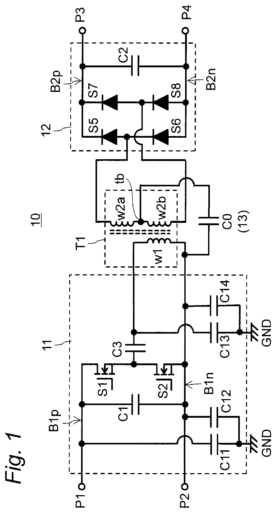
is a circuit diagram illustrating a configuration of a power conversion apparatus 10 according to a first embodiment.
is a circuit diagram illustrating a configuration of a power conversion apparatus 10 A according to a first modified embodiment of the first embodiment.
is a circuit diagram illustrating a configuration of a power conversion apparatus 10 B according to a second modified embodiment of the first embodiment.
is a circuit diagram illustrating a configuration of a power conversion apparatus 10 C according to a third modified embodiment of the first embodiment.
is a circuit diagram illustrating a configuration of a power conversion apparatus 10 D according to a fourth modified embodiment of the first embodiment.
is a circuit diagram illustrating a configuration of a power conversion apparatus 20 according to a second embodiment.
is a circuit diagram illustrating a configuration of a power conversion apparatus 20 A according to a first modified embodiment of the second embodiment.
is a circuit diagram illustrating a configuration of a power conversion apparatus 20 B according to a second modified embodiment of the second embodiment.
is a circuit diagram illustrating a configuration of a power conversion apparatus 20 C according to a third modified embodiment of the second embodiment.
is a circuit diagram illustrating a configuration of a power conversion apparatus 30 according to a third embodiment.
is a circuit diagram illustrating a configuration of a power conversion apparatus 30 A according to a first modified embodiment of the third embodiment.
is a circuit diagram illustrating a configuration of a power conversion apparatus 30 B according to a second modified embodiment of the third embodiment.
is a circuit diagram illustrating a configuration of a power conversion apparatus 30 C according to a third modified embodiment of the third embodiment.
is a block diagram illustrating a configuration of a power unit according to an implementation example.
is a circuit diagram illustrating a configuration of a stabilization circuit 42 of .
is a circuit diagram illustrating a configuration of an input filter 43 of .
is a circuit diagram illustrating a configuration of an output filter 45 of .
is a graph illustrating frequency characteristics of common mode noise occurring in a power unit including a power conversion apparatus according to a first implementation example.
is a graph illustrating frequency characteristics of common mode noise occurring in a power unit including a power conversion apparatus according to a second implementation example.
is a graph illustrating the characteristics of common mode noise occurring in the power unit including the power conversion apparatus according to the second implementation example, with respect to the capacitance of a capacitor C 0 of the power unit.
is a graph illustrating frequency characteristics of common mode noise occurring in a power unit including a power conversion apparatus according to a third implementation example.
is a graph illustrating frequency characteristics of common mode noise occurring in a power unit including a power conversion apparatus according to a fourth implementation example.
is a graph illustrating frequency characteristics of common mode noise occurring in a power unit including a power conversion apparatus according to a fifth implementation example.
is a graph illustrating the characteristics of common mode noise occurring in the power unit including the power conversion apparatus according to the fifth implementation example, with respect to the capacitance of a capacitor C 0 of the power unit.
is a graph illustrating frequency characteristics of common mode noise occurring in a power unit including a power conversion apparatus according to a sixth implementation example.
is a graph illustrating frequency characteristics of common mode noise occurring in a power unit including a power conversion apparatus according to a seventh implementation example.
is a graph illustrating the characteristics of common mode noise occurring in the power unit including the power conversion apparatus according to the seventh implementation example, with respect to the capacitance of a capacitor C 0 of the power unit.
is a graph illustrating frequency characteristics of common mode noise occurring in a power unit including a power conversion apparatus according to an eighth implementation example.
DESCRIPTION OF EMBODIMENTS
Hereinafter, embodiments of the present disclosure will be described with reference to the drawings. In the drawings, the same reference numerals denote similar components.
First Embodiment
is a circuit diagram illustrating a configuration of a power conversion apparatus 10 according to a first embodiment. The power conversion apparatus 10 is provided with a transformer T 1 , a primary circuit 11 , and a secondary circuit 12 .
The transformer T 1 has a primary winding w 1 , and secondary windings w 2 a and w 2 b with a center tap tb.
The primary circuit 11 of the power conversion apparatus 10 is connected to the primary winding w 1 of the transformer T 1 . The primary circuit 11 of the power conversion apparatus 10 is provided with a primary positive bus B 1 p , a primary negative bus B 1 n , capacitors C 1 and C 3 , and switching elements S 1 and S 2 . A DC voltage is inputted to the positive bus B 1 p and the negative bus B 1 n from an external DC power supply apparatus through terminals P 1 and P 2 . The capacitor C 1 smooths the inputted DC voltage. The switching elements S 1 and S 2 are connected in series between the positive bus B 1 p and the negative bus B 1 n to constitute a half-bridge inverter. The switching elements S 1 and S 2 are transistors. A node between the switching elements S 1 and S 2 is connected to one end of the primary winding w 1 of the transformer T 1 through a capacitor C 3 . The primary winding w 1 of the transformer T 1 , a leakage inductance of the transformer T 1 , and the capacitor C 3 constitute an LLC resonance circuit. The LLC resonance circuit may further include a resonant inductor connected in series with the capacitor C 3 and the primary winding w 1 of the transformer T 1 .
The power conversion apparatus 10 may be provided with a ground conductor GND. In this case, the positive bus B 1 p and the negative bus B 1 n may be capacitively coupled to the ground conductor GND. This capacitance is also referred to as “Y capacitors”. The example of illustrates a case where the positive bus B 1 p and the negative bus B 1 n are connected to the ground conductor GND through capacitors C 11 and C 12 , respectively.
In addition, both ends of the primary winding w 1 of the transformer T 1 may be capacitively coupled to the ground conductor GND. The example of illustrates a case where wirings at both ends of the primary winding w 1 of the transformer T 1 are connected to the ground conductor GND through capacitors C 13 and C 14 , respectively. In addition, the primary winding w 1 of the transformer T 1 may be capacitively coupled to the secondary windings w 2 a and w 2 b of the transformer T 1 .
The secondary circuit 12 of the power conversion apparatus 10 is connected to the secondary windings w 2 a and w 2 b of the transformer T 1 . The secondary circuit 12 of the power conversion apparatus 10 is provided with a secondary positive bus B 2 p , a secondary negative bus B 2 n , a capacitor C 2 , and switching elements S 5 to S 8 . The switching elements S 5 to S 8 are, for example, diodes, and they constitute a full-bridge rectifier circuit. Input terminals of the rectifier circuit are connected to the secondary windings w 2 a and w 2 b of the transformer T 1 , and output terminals of the rectifier circuit are connected to the positive bus B 2 p and the negative bus B 2 n . The capacitor C 2 smooths the voltage outputted from the rectifier circuit. The positive bus B 2 p and the negative bus B 2 n are connected to an external load apparatus through terminals P 3 and P 4 , and the smoothed voltage is outputted to the load apparatus.
The secondary circuit 12 of the power conversion apparatus 10 may be provided with transistor switching elements, instead of the diode switching elements S 5 to S 8 . In this case, the switching elements constitute a full-bridge synchronous rectifier circuit.
The power conversion apparatus 10 is further provided with a coupling circuit 13 including a capacitor C 0 . The coupling circuit 13 (i.e., capacitor C 0 ) is connected between the center tap tb of the secondary windings of the transformer T 1 , and the primary negative bus B 1 n.
According to the first embodiment, the power conversion apparatus 10 is configured such that the primary circuit 11 is an unbalanced circuit and the secondary circuit 12 is a balanced circuit. As described above, in a case where the power conversion apparatus is provided with an unbalanced circuit and a balanced circuit, which are not matched with each other, common mode noise occurs when power is inputted from the unbalanced circuit to the balanced circuit. In the case of transmitting communication signals, it has been known that when two transmission lines having different degrees of balance are connected to each other, the transmission lines have different reference voltage potentials, and therefore, mode conversion occurs at their connection point. Therefore, by making the reference voltage potentials of the primary circuit 11 and the secondary circuit 12 the same with each other, it is possible to match the degrees of balance of the primary circuit 11 and the secondary circuit 12 with each other. According to the first embodiment, since the capacitor C 0 is used, the transformer T 1 serves as a balun to be used in a transmission line for communication, and therefore, it is possible to match the reference voltage potentials of the primary circuit 11 and the secondary circuit 12 with each other. The capacitor C 0 is used because it is necessary for the power conversion apparatus to keep the primary circuit 11 and the secondary circuit 12 isolated from each other. As a result, it is possible to match the degrees of balance between the primary circuit 11 and the secondary circuit 12 with each other, and reduce common mode noise than that of a case without the capacitor C 0 (opened).
In the case where the primary circuit 11 includes the Y capacitors (i.e., capacitors C 11 and C 12 ), the capacitance of the capacitor C 0 is preferably set to be larger than the capacitance of the Y capacitors. The larger the capacitance of the capacitor C 0 , the greater the effect of reducing common mode noise. When the capacitance of the capacitor C 0 is larger than the capacitance of the Y capacitors, common mode noise is significantly reduced. On the other hand, in the case where the secondary circuit 12 includes the Y capacitors, the effect of reducing common mode noise by the capacitor C 0 is not much affected by the capacitance of the Y capacitors of the secondary circuit 12 .
As described above, according to the power conversion apparatus 10 of the first embodiment, it is possible to reduce common mode noise than that of prior art, with simple additional components.
In order to reduce common mode noise using a conventional noise filter to the extent equivalent to that of the power conversion apparatus according to the embodiment of the present disclosure, a large noise filter is required. On the other hand, according to the power conversion apparatus 10 of the first embodiment, it is possible to reduce common mode noise by providing only the capacitor C 0 , without need of other noise reduction components. Hence, it is possible to provide a small-sized and low-cost power conversion apparatus.
According to the power conversion apparatus 10 of the first embodiment, even when the power conversion apparatus includes an LLC resonance circuit, it is possible to make large common mode noise less likely to occur.
Hereinafter, modified embodiments of the first embodiment will be described.
is a circuit diagram illustrating a configuration of a power conversion apparatus 10 A according to a first modified embodiment of the first embodiment. The power conversion apparatus 10 A is provided with a coupling circuit 13 A including a capacitor C 0 and a resistor R 0 connected in series, instead of the coupling circuit 13 of the power conversion apparatus 10 of (i.e., capacitor C 0 ). A center tap tb of secondary windings of a transformer T 1 is connected to a primary negative bus B 1 n through the capacitor C 0 and the resistor R 0 connected in series. Since the resistor R 0 is used, even if an unwanted parasitic component occurs in the power conversion apparatus 10 A, or even if there are variations in components, it is possible to make the circuit less likely to resonate. In addition, since the resistor R 0 is used, it is possible to make common mode noise less likely to increase in high frequency bands. Therefore, according to the power conversion apparatus 10 A of , it is possible to reliably reduce common mode noise over a wide frequency band.
is a circuit diagram illustrating a configuration of a power conversion apparatus 10 B according to a second modified embodiment of the first embodiment. The power conversion apparatus 10 B is provided with a coupling circuit 13 B including a capacitor C 0 , a resistor R 0 , and an inductor L 0 connected in series, instead of the coupling circuit 13 of the power conversion apparatus 10 of (i.e., capacitor C 0 ). A center tap tb of secondary windings of a transformer T 1 is connected to a primary negative bus Bin through the capacitor C 0 , the resistor R 0 , and the inductor L 0 connected in series. According to the power conversion apparatus 10 B of , it is possible to reduce common mode noise in a desired frequency band by configuring the resonance circuit of the capacitor C 0 , the resistor R 0 , and the inductor L 0 .
is a circuit diagram illustrating a configuration of a power conversion apparatus 10 C according to a third modified embodiment of the first embodiment. The power conversion apparatus 10 C is provided with a primary circuit 11 C, instead of the primary circuit 11 of the power conversion apparatus 10 of . The primary circuit 11 C is provided with capacitors C 21 and C 22 and inductors L 21 and L 22 , instead of the capacitor C 3 of . The inductor L 21 , the capacitor C 21 , and the inductor L 22 are connected in series between a primary winding w 1 of a transformer T 1 , and switching elements S 1 and S 2 of the primary circuit 11 C. In addition, the capacitor C 22 is connected in parallel to the inductor L 22 . The inductor L 21 and the capacitor C 21 constitute a series resonance circuit, and the inductor L 22 and the capacitor C 22 constitute a parallel resonance circuit. Further, the primary winding w 1 of the transformer T 1 , the capacitors C 21 and C 22 , and the inductors L 21 and L 22 constitute a resonance circuit (also referred to as “LLCLC resonance circuit”). By using such a resonance circuit for soft switching, it is possible to reduce loss and improve power density of the power conversion apparatus.
In addition, the power conversion apparatus 10 C may include the coupling circuit 13 A of or the coupling circuit 13 B of , instead of the coupling circuit 13 of .
is a circuit diagram illustrating a configuration of a power conversion apparatus 10 D according to a fourth modified embodiment of the first embodiment. In the power conversion apparatus according to the first embodiment, a coupling circuit 13 (i.e., capacitor C 0 ) may be connected between a center tap tb of secondary windings of a transformer T 1 , and a primary positive bus B 1 p . Also in the case where the center tap tb is connected to the positive bus B 1 p , it is possible to reduce common mode noise to the extent equivalent to that of the case where the center tap tb is connected to the negative bus B 1 n.
In addition, the power conversion apparatus 10 D may include the coupling circuit 13 A of or the coupling circuit 13 B of , instead of the coupling circuit 13 of .
In addition, according to the first embodiment, the coupling circuit may be configured to include only the capacitor C 0 and the inductor L 0 connected in series.
In addition, according to the first embodiment, the primary circuit is not limited to the circuit including the two switching elements S 1 and S 2 , and may be an unbalanced circuit including one, three, or more switching elements.
In addition, according to the first embodiment, the primary circuit may be an unbalanced circuit in which one of the positive bus B 1 p and the negative bus Bin is grounded.
Second Embodiment
is a circuit diagram illustrating a configuration of a power conversion apparatus 20 according to a second embodiment. The power conversion apparatus 20 is provided with a transformer T 2 , a primary circuit 21 , and a secondary circuit 22 .
The transformer T 2 has primary windings w 1 a and w 1 b with a center tap ta, and has secondary windings w 2 a and w 2 b with a center tap tb.
The primary circuit 21 of the power conversion apparatus 20 is connected to the primary windings w 1 a and w 1 b of the transformer T 2 . The primary circuit 21 of the power conversion apparatus 20 is provided with a primary positive bus B 1 p , a primary negative bus B 1 n , capacitors C 1 , C 5 , and C 6 , and switching elements S 1 to S 4 . A DC voltage is inputted to the positive bus B 1 p and the negative bus Bin from an external DC power supply apparatus. The capacitor C 1 smooths the inputted DC voltage. The switching elements S 1 to S 4 are transistors, and constitute a full-bridge inverter. Input terminals of the inverter are connected to the positive bus B 1 p and the negative bus B 1 n , respectively, and output terminals of the inverter is connected to both ends of the primary windings w 1 a and w 1 b of the transformer T 2 through the capacitors C 5 and C 6 , respectively. The primary windings w 1 a and w 1 b of the transformer T 2 , the leakage inductance of the transformer T 2 , and the capacitors C 5 and C 6 constitute an LLC resonance circuit. The LLC resonance circuit may further include a resonant inductor connected in series with the capacitors C 5 , C 6 and the primary windings w 1 a and w 1 b of the transformer T 2 .
The power conversion apparatus 20 may be provided with a ground conductor GND. In this case, the positive bus B 1 p and the negative bus B 1 n may be capacitively coupled to the ground conductor GND. This capacitance is also referred to as “Y capacitors”. The example of illustrates a case where the positive bus B 1 p and the negative bus B 1 n are connected to the ground conductor GND through capacitors C 11 and C 12 , respectively.
In addition, both ends of the primary windings w 1 a and w 1 b of the transformer T 2 may be capacitively coupled to the ground conductor GND. In addition, the primary windings w 1 a and w 1 b of the transformer T 2 may be capacitively coupled to the secondary windings w 2 a and w 2 b of the transformer T 2 .
The secondary circuit 22 of the power conversion apparatus 20 is connected to the secondary windings w 2 a and w 2 b of the transformer T 2 . The secondary circuit 22 of the power conversion apparatus 20 is provided with a secondary positive bus B 2 p , a secondary negative bus B 2 n , a capacitor C 2 , and switching elements S 5 and S 6 . The switching elements S 5 and S 6 are, for example, diodes, and constitute a half-bridge rectifier circuit. The anodes of the switching elements S 5 and S 6 are connected to both ends of the secondary windings w 2 a and w 2 b of the transformer T 2 , and the cathodes of the switching elements S 5 and S 6 are connected to the positive bus B 2 p . The center tap tb of the secondary windings of the transformer T 2 is connected to the negative bus B 2 n . The capacitor C 2 smooths the voltage outputted from the rectifier circuit. The positive bus B 2 p and the negative bus B 2 n are connected to an external load apparatus, and the smoothed voltage is outputted to the load apparatus.
The secondary circuit 22 of the power conversion apparatus 20 may be provided with transistor switching elements, instead of the diode switching elements S 5 and S 6 . In this case, the switching elements constitute a half-bridge synchronous rectifier circuit.
The power conversion apparatus 20 is further provided with a coupling circuit 23 including a capacitor C 0 . The coupling circuit 23 is connected between the center tap to of the primary windings of the transformer T 2 , and the secondary negative bus B 2 n.
According to the second embodiment, the power conversion apparatus 20 is configured such that the primary circuit 21 is a balanced circuit and the secondary circuit 22 is an unbalanced circuit. According to the second embodiment, since the capacitor C 0 is used, the transformer T 2 serves as a balun, and therefore, it is possible to match the reference voltage potentials of the primary circuit 21 and the secondary circuit 22 with each other, while keeping the primary circuit 21 and the secondary circuit 22 isolated from each other, in a manner similar to that of the first embodiment. As a result, it is possible to match the degrees of balance between the primary circuit 21 and the secondary circuit 22 with each other, and reduce common mode noise than that of a case without the capacitor C 0 .
Also in the second embodiment, in the case where the primary circuit 21 includes the Y capacitors (i.e., capacitors C 11 and C 12 ), the capacitance of the capacitor C 0 is preferably set to be larger than the capacitance of the Y capacitors, in a manner similar to that of the first embodiment. The larger the capacitance of the capacitor C 0 , the greater the effect of reducing common mode noise. When the capacitance of the capacitor C 0 is larger than the capacitance of the Y capacitors, common mode noise is significantly reduced. On the other hand, in the case where the secondary circuit 22 includes the Y capacitors, the effect of reducing common mode noise by the capacitor C 0 is not much affected by the capacitance of the Y capacitors of the secondary circuit 22 .
As described above, according to the power conversion apparatus 20 of the second embodiment, it is possible to reduce common mode noise than that of prior art, with simple additional components.
According to the power conversion apparatus 20 of the second embodiment, it is possible to reduce common mode noise by providing only the capacitor C 0 , without need of other noise reduction components. Hence, it is possible to provide a small-sized and low-cost power conversion apparatus.
According to the power conversion apparatus 20 of the second embodiment, even when the power conversion apparatus includes an LLC resonance circuit, it is possible to make large common mode noise less likely to occur.
Hereinafter, modified embodiments of the second embodiment will be described.
is a circuit diagram illustrating a configuration of a power conversion apparatus 20 A according to a first modified embodiment of the second embodiment. The power conversion apparatus 20 A is provided with a coupling circuit 23 A including a capacitor C 0 and a resistor R 0 connected in series, instead of the coupling circuit 23 of the power conversion apparatus 20 of (i.e., capacitor C 0 ). A center tap ta of primary windings of a transformer T 2 is connected to a secondary negative bus B 2 n through the capacitor C 0 and the resistor R 0 connected in series. Since the resistor R 0 is used, even if an unwanted parasitic component occurs in the power conversion apparatus 20 A, or even if there are variations in components, it is possible to make the circuit less likely to resonate. In addition, since the resistor R 0 is used, it is possible to make common mode noise less likely to increase in high frequency bands. Therefore, according to the power conversion apparatus 20 A of , it is possible to reliably reduce common mode noise over a wide frequency band.
is a circuit diagram illustrating a configuration of a power conversion apparatus 20 B according to a second modified embodiment of the second embodiment. The power conversion apparatus 20 B is provided with a coupling circuit 23 B including a capacitor C 0 , a resistor R 0 , and an inductor L 0 connected in series, instead of the coupling circuit 23 of the power conversion apparatus 20 of (i.e., capacitor C 0 ). A center tap ta of primary windings of a transformer T 2 is connected to a secondary negative bus B 2 n through the capacitor C 0 , the resistor R 0 , and the inductor L 0 connected in series. According to the power conversion apparatus 20 B of , it is possible to reduce common mode noise in a desired frequency band by configuring the resonance circuit of the capacitor C 0 , the resistor R 0 , and the inductor L 0 . In addition, according to the power conversion apparatus 20 B of , external noise such as lightning surge is less likely to be transmitted between the primary circuit 21 and the secondary circuit 22 , and therefore, the noise-resistant performance is improved.
is a circuit diagram illustrating a configuration of a power conversion apparatus 20 C according to a third modified embodiment of the second embodiment. In the power conversion apparatus according to the second embodiment, a coupling circuit 23 (i.e., capacitor C 0 ) may be connected between a center tap ta of primary windings of a transformer T 2 , and a positive bus B 2 p . Also in the case where the center tap ta is connected to the positive bus B 2 p , it is possible to reduce common mode noise to the extent equivalent to the case where the center tap ta is connected to the negative bus B 2 n.
In addition, the power conversion apparatus 20 C may be provided with the coupling circuit 23 A of or the coupling circuit 23 B of , instead of the coupling circuit 23 of .
In addition, according to the second embodiment, the coupling circuit may be configured to include only the capacitor C 0 and the inductor L 0 connected in series.
In addition, according to the second embodiment, the secondary circuit is not limited to the circuit including the two switching elements S 5 and S 6 , and may be an unbalanced circuit including one, three, or more switching elements.
In addition, according to the second embodiment, the secondary circuit may be an unbalanced circuit in which one of the positive bus B 2 p and the negative bus B 2 n is grounded.
Third Embodiment
is a circuit diagram illustrating a configuration of a power conversion apparatus 30 according to a third embodiment. The power conversion apparatus 30 is provided with a transformer T 2 , a primary circuit 31 , and a secondary circuit 32 .
The transformer T 2 has primary windings w 1 a and w 1 b with a center tap ta, and has secondary windings w 2 a and w 2 b with a center tap tb.
The primary circuit 31 of the power conversion apparatus 30 is configured in a manner similar to that of the primary circuit 21 of the power conversion apparatus 20 of . The example of illustrates a case where wirings at both ends of the primary windings w 1 a and w 1 b of the transformer T 2 are connected to a ground conductor GND through capacitors C 13 and C 14 , respectively.
The secondary circuit 32 of the power conversion apparatus 30 is configured in a manner similar to that of the secondary circuit 12 of the power conversion apparatus 10 of .
The power conversion apparatus 30 is further provided with a coupling circuit 33 including a capacitor C 0 . The coupling circuit 33 (i.e., capacitor C 0 ) is connected between the center tap ta of the primary windings of the transformer T 2 , and the center tap tb of the secondary windings of the transformer T 2 .
According to the third embodiment, the power conversion apparatus 30 is configured such that the primary circuit 31 is a balanced circuit and the secondary circuit 32 is a balanced circuit. As described above, even when the power conversion apparatus is provided with the balanced primary circuit 31 and the balanced secondary circuit 32 , imbalance due to parasitic components of the circuits may generate common mode noise. For example, in a case where the capacitances of the capacitors C 13 and C 14 are different from each other, the balance is broken. It is assumed that the capacitors C 13 and C 14 are parasitic capacitances occurring between the transformer T 2 and the heat sink (GND). It can be said that the balance is broken in many transformers unless their physical structure is perfectly symmetrical. According to the third embodiment, since the capacitor C 0 is used, the transformer T 2 serves as a balun, and therefore, it is possible to match the reference voltage potentials of the primary circuit 31 and the secondary circuit 32 with each other, while keeping the primary circuit 31 and the secondary circuit 32 isolated from each other, in a manner similar to that of the first and second embodiments. As a result, it is possible to match the degrees of balance between the primary circuit 31 and the secondary circuit 32 with each other, and reduce common mode noise than that of a case without the capacitor C 0 .
Also in the third embodiment, in the case where the primary circuit 31 includes the Y capacitors (i.e., capacitors C 11 and C 12 ), the capacitance of the capacitor C 0 is preferably set to be larger than the capacitance of the Y capacitors, in a manner similar to that of the first embodiment. The larger the capacitance of the capacitor C 0 , the greater the effect of reducing common mode noise. When the capacitance of the capacitor C 0 is larger than the capacitance of the Y capacitors, common mode noise is significantly reduced. On the other hand, in the case where the secondary circuit 32 includes the Y capacitors, the effect of reducing the common mode noise by the capacitor C 0 is not much affected by the capacitance of the Y capacitors of the secondary circuit 32 .
As described above, according to the power conversion apparatus 30 of the third embodiment, it is possible to reduce common mode noise than that of prior art, with simple additional components.
According to the power conversion apparatus 30 of the third embodiment, it is possible to reduce common mode noise by providing only the capacitor C 0 , without need of other noise reduction components. Hence, it is possible to provide a small-sized and low-cost power conversion apparatus.
According to the power conversion apparatus 30 of the third embodiment, even when the power conversion apparatus includes an LLC resonance circuit, it is possible to make large common mode noise less likely to occur.
Hereinafter, modified embodiments of the third embodiment will be described.
is a circuit diagram illustrating a configuration of a power conversion apparatus 30 A according to a first modified embodiment of the third embodiment. The power conversion apparatus 30 A is provided with a coupling circuit 33 A including a capacitor C 0 and a resistor R 0 connected in series, instead of the coupling circuit 33 of the power conversion apparatus 30 of (i.e., capacitor C 0 ). A center tap ta of primary windings of a transformer T 2 is connected to a center tap tb of secondary windings of the transformer T 2 through the capacitor C 0 and the resistor R 0 connected in series. Since the resistor R 0 is used, even if an unwanted parasitic component occurs in the power conversion apparatus 30 A, or even if there are variations in components, it is possible to make the circuit less likely to resonate. In addition, since the resistor R 0 is used, it is possible to make common mode noise less likely to increase in high frequency bands. Therefore, according to the power conversion apparatus 30 A of , it is possible to reliably reduce common mode noise over a wide frequency band.
is a circuit diagram illustrating a configuration of a power conversion apparatus 30 B according to a second modified embodiment of the third embodiment. The power conversion apparatus 30 B is provided with a coupling circuit 33 B including a capacitor C 0 , a resistor R 0 , and an inductor L 0 connected in series, instead of the coupling circuit 33 of the power conversion apparatus 30 of (i.e., capacitor C 0 ). A center tap ta of primary windings of a transformer T 2 is connected to a center tap tb of secondary windings of the transformer T 2 through the capacitor C 0 , the resistor R 0 , and the inductor L 0 connected in series. According to the power conversion apparatus 30 B of , it is possible to reduce common mode noise in a desired frequency band by configuring the resonance circuit of the capacitor C 0 , the resistor R 0 , and the inductor L 0 .
is a circuit diagram illustrating a configuration of a power conversion apparatus 30 C according to a third modified embodiment of the third embodiment. The power conversion apparatus 30 C is provided with a secondary circuit 32 C, instead of the secondary circuit 32 of the power conversion apparatus 30 of . The secondary circuit 32 C is provided with transistor switching elements S 5 A to S 8 A, instead of the diode switching elements S 5 to S 8 of . The secondary circuit 32 C is further provided with capacitors C 7 and C 8 connected between both ends of secondary windings w 2 a and w 2 b of the transformer T 2 , and the switching elements S 5 A to S 8 A of the secondary circuit, respectively. Switching elements S 1 to S 4 of a primary circuit 31 operate as an inverter, and also operate as a synchronous rectifier circuit. The switching elements S 5 A to S 8 A of the secondary circuit 32 C operate as an inverter, and also operate as a synchronous rectifier circuit. As a result, the power conversion apparatus 30 C operates as a “reversible” power conversion apparatus configured to convert a voltage inputted from the primary side into a predetermined voltage and output the voltage from the secondary side, and also configured to convert a voltage inputted from the secondary side into a predetermined voltage and output the voltage from the primary side. Capacitors C 5 and C 6 , the primary windings w 1 a and w 1 b and the secondary windings w 2 a and w 2 b of the transformer T 2 , and the capacitors C 7 and C 8 constitute a resonance circuit (also referred to as “CLLC resonance circuit”). By using such a resonance circuit for soft switching, it is possible to reduce loss and improve power density of the power conversion apparatus.
Implementation Examples
Hereinafter, simulation results of power conversion apparatuses according to implementation examples of the present disclosure will be described with reference to to 28 .
is a block diagram illustrating a configuration of a power unit according to the implementation example. The power unit is provided with a DC power supply apparatus 41 , a stabilization circuit 42 , an input filter 43 , a power conversion apparatus 44 , an output filter 45 , and a load apparatus 46 .
The DC power supply apparatus 41 supplies a predetermined DC voltage.
is a circuit diagram illustrating a configuration of the stabilization circuit 42 of . The stabilization circuit 42 is provided with capacitors C 101 and C 102 , inductors L 101 and L 102 , and resistors R 101 and R 102 . The stabilization circuit 42 stabilizes impedance at terminals through which power is inputted to the power conversion apparatus 44 , in order to accurately measure common mode noise generated by the power conversion apparatus 44 . In the simulations described below, we calculated common mode noise in the stabilization circuit 42 .
is a circuit diagram illustrating a configuration of the input filter 43 of . The input filter 43 is provided with capacitors C 111 to C 114 and a common mode choke coil L 111 .
The power conversion apparatus 44 is any of the power conversion apparatuses described in the first to third embodiments.
is a circuit diagram illustrating a configuration of the output filter 45 of . The output filter 45 is provided with capacitors C 121 to C 126 and a common mode choke coil L 121 .
The load apparatus 46 has a predetermined resistance.
Next, simulation results of the power conversion apparatuses according to the first embodiment will be described with reference to to 21 . Here, we conducted simulations for a case where the power conversion apparatus 44 is the power conversion apparatus 10 of , the power conversion apparatus 10 A of , or the power conversion apparatus 10 B of .
For the simulations of to 21 , the following parameters were set.
(DC Power Supply Apparatus 41 )
•
• Input voltage: 400 V (Input Filter 43 ) • Capacitance of capacitors C 111 and C 112 : 2 μF • Capacitance of capacitors C 113 and C 114 : 1 nF • Inductance of common mode choke coil L 111 : 3 mH • Coupling coefficient of common mode choke coil L 111 : 0.9995 (Power Conversion Apparatus 44 ) • Capacitance of capacitor C 1 : 100 μF • Capacitance of capacitor C 2 : 10 μF • Capacitance of capacitor C 3 : 22.5 nF • Capacitance of capacitors C 11 and C 12 : 1 nF • Capacitance of capacitors C 13 and C 14 : 10 pF • Inductance of primary winding w 1 of transformer T 1 : 120 μH • Inductance of secondary windings w 2 a and w 2 b of transformer T 1 : 6.6 μH • Coupling coefficient of transformer T 1 : 0.94 • Switching frequency of switching elements S 1 and S 2 : 200 kHz (Output filter 45 ) • Capacitance of capacitors C 121 and C 122 : 2 μF • Capacitance of capacitors C 123 to C 126 : 10 nF • Inductance of common mode choke coil L 121 : 3 mH • Coupling coefficient of common mode choke coil L 121 : 0.9995 (Load apparatus 46 ) • Resistance of load apparatus 46 : 10 Ω
is a graph illustrating frequency characteristics of common mode noise occurring in the power unit including the power conversion apparatus according to the first implementation example. Referring to , the first implementation example illustrates a case where a power conversion apparatus 44 is the power conversion apparatus 10 of , and the capacitance of a capacitor C 0 is set to 100 nF. In addition, referring to , a comparison example illustrates a case where the capacitor C 0 is removed. According to , the frequency characteristics of common mode noise are observed as a spectrum with peaks at integral multiples of the switching frequency. In addition, according to , it can be seen that common mode noise can be reduced by 14.7 dB at the switching frequency of 200 kHz. In addition, according to , it can be seen that harmonic common mode noise up to about 5 MHz can also be reduced.
is a graph illustrating frequency characteristics of common mode noise occurring in a power unit including a power conversion apparatus according to a second implementation example. Referring to , the second implementation example illustrates a case where a power conversion apparatus 44 is the power conversion apparatus 10 A of , the capacitance of a capacitor C 0 is set to 100 nF, and the resistance of a resistor R 0 is set to 10Ω. In addition, referring to , a comparison example illustrates a case where the capacitor C 0 and the resistor R 0 are removed. According to , it can be seen that common mode noise can be reduced by 15.4 dB at the switching frequency of 200 kHz. In addition, according to , it can be seen that unwanted resonance at high frequencies is damped, and the common mode noise characteristics at high frequencies are improved as compared with the case of .
is a graph illustrating the characteristics of common mode noise occurring in the power unit including the power conversion apparatus according to the second implementation example, with respect to the capacitance of the capacitor C 0 of the power unit. illustrates a case where the power conversion apparatus 44 is the power conversion apparatus 10 A of , the capacitance of the capacitor C 0 is changed over 1 pF to 1 μF, and the resistance of the resistor R 0 is set to 10Ω. According to , it can be seen that when the capacitance of the capacitor C 0 exceeds the capacitances of the capacitors C 11 and C 12 (Y capacitors), the effect of reducing common mode noise increases.
is a graph illustrating frequency characteristics of common mode noise occurring in a power unit including a power conversion apparatus according to a third implementation example. Referring to , the third implementation example illustrates a case where a power conversion apparatus 44 is the power conversion apparatus 10 B of , the capacitance of a capacitor C 0 is set to 100 nF, the resistance of a resistor R 0 is set to 10Ω, and the inductance of an inductor L 0 is set to 9.4 μH. In addition, referring to , a comparison example illustrates a case where the capacitor C 0 , the resistor R 0 , and the inductor L 0 are removed. According to , it can be seen that common mode noise can be reduced by 26.1 dB at the switching frequency of 200 kHz. In addition, according to , it can be seen that although common mode noise can be effectively reduced only in limited frequency bands, it can be more effectively reduced in a specific frequency band.
Next, simulation results of the power conversion apparatuses according to the second embodiment will be described with reference to to 24 . Here, we conducted simulations for a case where the power conversion apparatus 44 is the power conversion apparatus 20 of or the power conversion apparatus 20 A of .
For the simulations of to 24 , the following parameters were set.
(DC power supply apparatus 41 )
•
• Input voltage: 200 V (Power conversion apparatus 44 ) • Capacitance of capacitor C 1 : 100 μF • Capacitance of capacitor C 2 : 10 μF • Capacitance of capacitors C 5 and C 6 : 45 nF • Capacitance of capacitors C 11 and C 12 : 1 nF • Inductance of primary windings w 1 a and w 1 b of transformer T 2 : 30 μH • Inductance of secondary windings w 2 a and w 2 b of transformer T 2 : 26.4 μH • Coupling coefficient of transformer T 2 : 0.94 • Switching frequency of switching elements S 1 and S 2 : 200 kHz
For the simulations of to 24 , a capacitance of 10 pF was further set between a terminal of a primary winding w 1 b of a transformer T 2 (i.e., node between primary winding w 1 b and capacitor C 6 ) and a center tap tb of secondary windings of the transformer T 2 .
For the simulations of to 24 , the same parameters of an input filter 43 , an output filter 45 , and a load apparatus 46 were set as those of the cases of to 21 .
is a graph illustrating frequency characteristics of common mode noise occurring in a power unit including a power conversion apparatus according to a fourth implementation example. Referring to , the fourth implementation example illustrates a case where a power conversion apparatus 44 is the power conversion apparatus 20 of , and the capacitance of a capacitor C 0 is set to 30 nF. In addition, referring to , a comparison example illustrates a case where the capacitor C 0 is removed. According to , it can be seen that common mode noise can be reduced by 16.5 dB at the switching frequency of 200 kHz.
is a graph illustrating frequency characteristics of common mode noise occurring in a power unit including a power conversion apparatus according to a fifth implementation example. Referring to , the fifth implementation example illustrates a case where a power conversion apparatus 44 is the power conversion apparatus 20 A of , the capacitance of a capacitor C 0 is set to 30 nF, and the resistance of a resistor R 0 is set to 100 CZ. In addition, referring to , a comparison example illustrates a case where the capacitor C 0 and the resistor R 0 are removed. According to , it can be seen that common mode noise can be reduced by 14.8 dB at the switching frequency of 200 kHz. In addition, according to , it can be seen that unwanted resonance at high frequencies is damped, and the common mode noise characteristics at high frequencies are improved as compared with the case of .
is a graph illustrating the characteristics of common mode noise occurring in the power unit including the power conversion apparatus according to the fifth implementation example, with respect to the capacitance of the capacitor C 0 of the power unit. illustrates a case where the power conversion apparatus 44 is the power conversion apparatus 20 A of , the capacitance of the capacitor C 0 is changed over 1 pF to 1 μF, and the resistance of the resistor R 0 is set to 10Ω. According to , it can be seen that when the capacitance of the capacitor C 0 exceeds the capacitances of capacitors C 11 and C 12 (Y capacitors), the effect of reducing common mode noise increases.
Next, simulation results of the power conversion apparatuses according to the third embodiment will be described with reference to to 28 . Here, we conducted simulations for a case where the power conversion apparatus 44 is the power conversion apparatus 30 of , the power conversion apparatus 30 A of , or the power conversion apparatus 30 B of .
For the simulations of to 28 , the following parameters were set.
(Power conversion apparatus 44 )
•
• Capacitance of capacitor C 1 : 100 μF • Capacitance of capacitor C 2 : 10 μF • Capacitance of capacitors C 5 and C 6 : 45 nF • Capacitance of capacitors C 11 and C 12 : 1 nF • Capacitance of capacitor C 13 : 20 pF • Capacitance of capacitor C 14 : 10 pF • Inductance of primary windings w 1 a and w 1 b of transformer T 2 : 30 μH • Inductance of secondary windings w 2 a and w 2 b of transformer T 2 : 6.6 μH • Coupling coefficient of transformer T 2 : 0.94 • Switching frequency of switching elements S 1 and S 2 : 200 kHz
For the simulations of to 28 , the same parameters of a DC power supply apparatus 41 , an input filter 43 , an output filter 45 , and a load apparatus 46 were set as those of the cases of to 21 .
is a graph illustrating frequency characteristics of common mode noise occurring in a power unit including a power conversion apparatus according to a sixth implementation example. Referring to , the sixth implementation example illustrates a case where a power conversion apparatus 44 is the power conversion apparatus 30 of , and the capacitance of a capacitor C 0 is set to 100 nF. In addition, referring to , a comparison example illustrates a case where the capacitor C 0 is removed. According to , it can be seen that common mode noise can be reduced by 16.2 dB at the switching frequency of 200 kHz.
is a graph illustrating frequency characteristics of common mode noise occurring in a power unit including a power conversion apparatus according to a seventh implementation example. Referring to , the seventh implementation example illustrates a case where a power conversion apparatus 44 is the power conversion apparatus 30 A of , the capacitance of a capacitor C 0 is set to 100 nF, and the resistance of a resistor R 0 is set to 50Ω. In addition, referring to , a comparison example illustrates a case where the capacitor C 0 and the resistor R 0 are removed. According to , it can be seen that common mode noise can be reduced by 12.2 dB at the switching frequency of 200 kHz.
is a graph illustrating the characteristics of common mode noise occurring in the power unit including the power conversion apparatus according to the seventh implementation example, with respect to the capacitance of the capacitor C 0 of the power unit. illustrates a case where the power conversion apparatus 44 is the power conversion apparatus 30 A of , the capacitance of the capacitor C 0 is changed over 1 pF to 1 μF, and the resistance of the resistor R 0 is set to 10Ω. According to , it can be seen that when the capacitance of the capacitor C 0 exceeds the capacitances of capacitors C 11 and C 12 (Y capacitors), the effect of reducing common mode noise increases.
is a graph illustrating frequency characteristics of common mode noise occurring in a power unit including a power conversion apparatus according to an eighth implementation example. Referring to , the eighth implementation example illustrates a case where a power conversion apparatus 44 is the power conversion apparatus 30 B of , the capacitance of a capacitor C 0 is set to 100 nF, the resistance of a resistor R 0 is set to 10Ω, and the inductance of an inductor L 0 is set to 6.4 pH. In addition, referring to , a comparison example illustrates a case where the capacitor C 0 , the resistor R 0 , and the inductor L 0 are removed. According to , it can be seen that common mode noise can be reduced by 19.1 dB at the switching frequency of 200 kHz. In addition, according to , although common mode noise can be effectively reduced only in limited frequency bands, it can be more effectively reduced in a specific frequency band.
SUMMARY OF EMBODIMENTS
A power conversion apparatus according to a first aspect of the present disclosure is configured as follows.
According to the first aspect of the present disclosure, a power conversion apparatus is provided with a transformer, a primary circuit, and a secondary circuit. The primary circuit is configured as an unbalanced circuit, which is connected to a primary winding of the transformer, has a primary positive bus and a primary negative bus, and includes at least one switching element. The secondary circuit is configured as a balanced circuit, which is connected to a secondary winding of the transformer, has a secondary positive bus and a secondary negative bus, and includes a plurality of switching elements. The power conversion apparatus is further provided with a first capacitor connected between a center tap of the secondary winding of the transformer, and one of the primary positive bus and the primary negative bus.
According to the first aspect of the present disclosure, the power conversion apparatus is further provided with a ground conductor. The first capacitor has a capacitance larger than a capacitance between the ground conductor, and the primary positive bus and the primary negative bus.
According to the first aspect of the present disclosure, the power conversion apparatus is further provided with a resistor. The center tap of the secondary winding of the transformer is connected to one of the primary positive bus and the primary negative bus, through the first capacitor and the resistor connected in series.
According to the first aspect of the present disclosure, the power conversion apparatus is further provided with a first inductor. The center tap of the secondary winding of the transformer is connected to one of the primary positive bus and the primary negative bus, through the first capacitor and the first inductor connected in series.
According to the first aspect of the present disclosure, the primary circuit is a half-bridge circuit including two switching elements.
According to the first aspect of the present disclosure, the secondary circuit is a full-bridge circuit including four switching elements.
According to the first aspect of the present disclosure, the primary circuit further includes a second capacitor connected between the primary winding of the transformer and the switching element of the primary circuit.
According to the first aspect of the present disclosure, the primary circuit further includes second and third inductors connected in series to the second capacitor, and a third capacitor connected in parallel to the third inductor.
A power conversion apparatus according to a second aspect of the present disclosure is configured as follows.
According to the second aspect of the present disclosure, a power conversion apparatus is provided with a transformer, a primary circuit, and a secondary circuit. The primary circuit is configured as a balanced circuit, which is connected to a primary winding of the transformer, has a primary positive bus and a primary negative bus, and includes a plurality of switching elements. The secondary circuit is configured as an unbalanced circuit, which is connected to a secondary winding of the transformer, has a secondary positive bus and a secondary negative bus, and includes at least one switching element. The power conversion apparatus is further provided with a first capacitor connected between a center tap of the primary winding of the transformer, and one of the secondary positive bus and the secondary negative bus.
According to the second aspect of the present disclosure, the power conversion apparatus is further provided with a ground conductor. The first capacitor has a capacitance larger than a capacitance between the ground conductor, and the primary positive bus and the primary negative bus.
According to the second aspect of the present disclosure, the power conversion apparatus is further provided with a resistor. The center tap of the primary winding of the transformer is connected to one of the secondary positive bus and the secondary negative bus, through the first capacitor and the resistor connected in series.
According to the second aspect of the present disclosure, the power conversion apparatus is further provided with a first inductor. The center tap of the primary winding of the transformer is connected to one of the secondary positive bus and the secondary negative bus, through the first capacitor and the first inductor connected in series.
According to the second aspect of the present disclosure, the primary circuit is a full-bridge circuit including four switching elements.
According to the second aspect of the present disclosure, the secondary circuit is a half-bridge circuit including two switching elements.
According to the second aspect of the present disclosure, the primary circuit further includes second and third capacitors connected between both ends of the primary winding of the transformer, and the switching elements of the primary circuit, respectively.
A power conversion apparatus according to a third aspect of the present disclosure is configured as follows.
According to the third aspect of the present disclosure, a power conversion apparatus is provided with a transformer, a primary circuit, and a secondary circuit. The primary circuit is configured as a balanced circuit, which is connected to a primary winding of the transformer, has a primary positive bus and a primary negative bus, and includes a plurality of switching elements. The secondary circuit is configured as a balanced circuit, which is connected to a secondary winding of the transformer, has a secondary positive bus and a secondary negative bus, and includes a plurality of switching elements. The power conversion apparatus is further provided with a first capacitor connected between a center tap of the primary winding of the transformer, and a center tap of the secondary winding of the transformer.
According to the third aspect of the present disclosure, the power conversion apparatus is further provided with a ground conductor. The first capacitor has a capacitance larger than a capacitance between the ground conductor, and the primary positive bus and the primary negative bus.
According to the third aspect of the present disclosure, the power conversion apparatus is further provided with a resistor. The center tap of the primary winding of the transformer is connected to the center tap of the secondary winding of the transformer, through the first capacitor and the resistor connected in series.
According to the third aspect of the present disclosure, the power conversion apparatus is further provided with a first inductor. The center tap of the primary winding of the transformer is connected to the center tap of the secondary winding of the transformer, through the first capacitor and the first inductor connected in series.
According to the third aspect of the present disclosure, the primary circuit is a full-bridge circuit including four transistors as the plurality of switching elements.
According to the third aspect of the present disclosure, the secondary circuit is a full-bridge circuit including four diodes or four transistors as the plurality of switching elements.
According to the third aspect of the present disclosure, the primary circuit further includes second and third capacitors connected between both ends of the primary winding of the transformer, and the switching elements of the primary circuit, respectively.
According to the third aspect of the present disclosure, the secondary circuit further includes second and third capacitors connected between both ends of the secondary winding of the transformer, and the switching elements of the secondary circuit, respectively.
INDUSTRIAL APPLICABILITY
The power conversion apparatus according to the aspect of the present disclosure is applicable to, for example, an onboard charger, an onboard DC/DC converter, and the like.
REFERENCE SIGNS LIST
•
• 10 , 10 A to 10 D, 20 , 20 A to 20 C, 30 , 30 A to 30 C: POWER CONVERSION APPARATUS • 11 , 11 C, 21 , 31 : PRIMARY CIRCUIT • 12 , 22 , 32 , 32 C: SECONDARY CIRCUIT • 13 , 13 A, 13 B, 23 , 23 A, 23 B, 33 , 33 A, 33 B: COUPLING CIRCUIT • 41 : DC POWER SUPPLY APPARATUS • 42 : STABILIZATION CIRCUIT • 43 : INPUT FILTER • 44 : POWER CONVERSION APPARATUS • 45 : OUTPUT FILTER • 46 : LOAD APPARATUS • B 1 p , B 2 p : POSITIVE BUS • B 1 n , B 2 n : NEGATIVE BUS • C 0 , C 1 to C 8 , C 11 to C 14 , C 21 , C 22 : CAPACITOR • L 0 , L 21 , L 22 : INDUCTOR • R 0 : RESISTOR • S 1 to S 8 , S 5 A to SBA: SWITCHING ELEMENT • T 1 , T 2 : TRANSFORMER
Figures (20)
Citations
This patent cites (15)
- US2011/0242854
- US2012/0140525
- US2014/0268899
- US2017/0012548
- US2018/0074538
- US2019/0200441
- US2019/0319532
- US109643956
- USH08-033329
- USH11-122909
- US2004-040923
- US2007-097303
- US4672504
- US5633778
- US2017-077078