LLC Resonant Topology Control Circuit Based on Flyback Chip
Abstract
The present disclosure relates to an LLC resonant topology control circuit base on a flyback chip, including an LLC resonant cavity, a current mode flyback chip U 1 , a first drive circuit, a second drive circuit, a charge pump circuit and a feedback circuit, wherein the LLC resonant cavity includes a switching transistor Q 1 , a switching transistor Q 2 , a resonant inductor L 1 , a resonant capacitor C 1 and an output transformer T 1 ; the switching transistor Q 1 is connected in series with the switching transistor Q 2 ; the resonant inductor L 1 , a primary coil of the output transformer T 1 and the resonant capacitor C 1 are connected in series and then are connected in parallel to the switching transistor Q 2 . The LLC resonant topology control circuit provided by the present disclosure has the characteristics of low cost and small volume.
Claims (4)
1. An LLC resonant topology control circuit based on a flyback chip, comprising an LLC resonant cavity, a current mode flyback chip (U 1 ), a first drive circuit, a second drive circuit, a charge pump circuit and a feedback circuit, wherein the LLC resonant cavity comprises a switching transistor (Q 1 ), a switching transistor (Q 2 ), a resonant inductor (L 1 ), a resonant capacitor (C 1 ) and an output transformer (T 1 ); a drain of the switching transistor (Q 1 ) is connected to a VBUS end of a power supply; a source of the switching transistor (Q 1 ) is connected with a drain of the switching transistor (Q 2 ) and one end of the resonant inductor (L 1 ) respectively; the other end of the resonant inductor (L 1 ) is connected with one end of the resonant capacitor (C 1 ) through a primary coil of the output transformer (T 1 ), and the other end of the resonant capacitor (C 1 ) and a source of the switching transistor (Q 2 ) are connected with an LG end of the power supply; a gate of the switching transistor (Q 1 ) is connected with an output end of the first drive circuit; an input end of the first drive circuit is connected with a GD end of the current mode flyback chip (U 1 ); a gate of the switching transistor (Q 2 ) is connected with an output end of the second drive circuit; an input end of the second drive circuit is connected with an RT end of the current mode flyback chip (U 1 ); an input end of the second drive circuit is connected with a different end VD of an auxiliary winding of the transformer (T 1 ) through a resistor (R 6 ); one end of the resonant capacitor (C 1 ) is connected with a CS end of the current mode flyback chip (U 1 ) through the charge pump circuit; a secondary coil of the output transformer (T 1 ) is connected with an input end of the feedback circuit, and an output end of the feedback circuit is connected with an FB end of the current mode flyback chip (U 1 ) through an optically coupled isolator (U 2 ); the first drive circuit comprises triodes (Q 3 ) to (Q 6 ), a transformer (T 2 ), a diode (D 1 ), a capacitor (C 2 ) and resistors (R 2 ) to (R 4 ); the GD end of the current mode flyback chip (U 1 ) is connected with one end of the resistor (R 2 ), one end of the resistor (R 3 ) and an emitter of the triode (Q 5 ) through a resistor (R 1 ); the other end of the resistor (R 2 ) is connected with a base of the triode (Q 3 ) and a positive pole of the diode (D 1 ) respectively; a collector of the triode (Q 3 ) is connected with the other end of the resistor (R 3 ) and a base of the triode (Q 5 ) respectively through the resistor (R 4 ); a collector of the triode (Q 5 ) is connected with a base of the triode (Q 4 ) and a base of the triode (Q 6 ) respectively; an emitter of the triode (Q 6 ) is connected with an emitter of the triode (Q 4 ) and one end of a primary coil of the transformer (T 2 ) respectively; the other end of the primary coil of the transformer (T 2 ) is connected with one end of the capacitor (C 2 ); one end of a secondary coil of the transformer (T 2 ) is connected with a gate of the switching transistor (Q 1 ) through the resistor (R 5 ); the other end of the secondary coil of the transformer (T 2 ) is respectively connected with a negative pole of the diode (D 1 ) and one end of the resonant inductor (L 1 ); the other end of the capacitor (C 2 ), a collector of the triode (Q 4 ) and an emitter of the triode (Q 3 ) are all connected with the LG end of the power supply; a collector of the triode (Q 6 ) is connected with a VCC end of the power supply; the second drive circuit comprises triodes (Q 7 ) to (Q 9 ), a voltage stabilizing diode (ZD 1 ), a diode (D 2 ) and resistors (R 7 ) to (R 9 ); the RT end of the current mode flyback chip (U 1 ) is connected with one end of the resistor (R 7 ) through the resistor (R 6 ); the other end of the resistor (R 7 ) is respectively connected with a base of the triode (Q 7 ), a base of the triode (Q 8 ), a collector of the triode (Q 9 ) and a negative pole of the voltage stabilizing diode (ZD 1 ); an emitter of the triode (Q 8 ) is respectively connected with an emitter of the triode (Q 7 ) and one end of the resistor (R 8 ); a base of the triode (Q 9 ) is connected with one end of the resonant inductor (L 1 ) through the diode (D 2 ); the other end of the resistor (R 8 ) is connected with one end of the resistor (R 9 ) and a gate of the switching transistor (Q 2 ); the other end of the resistor (R 9 ), an emitter of the triode (Q 9 ), a collector of the triode (Q 7 ) and a positive pole of the voltage stabilizing diode (ZD 1 ) are all connected with the LG end of the power supply; and a collector of the triode (Q 8 ) is connected with the VCC end of the power supply.
Show 3 dependent claims
2. The LLC resonant topology control circuit based on the flyback chip according to claim 1 , wherein the charge pump circuit comprises a triode (Q 10 ), diodes (D 3 ) to (D 4 ), capacitors (C 3 ) to (C 6 ), and resistors (R 10 ) to (R 14 ); one end of the resonant capacitor (C 1 ) is respectively connected with one end of the resistor (R 10 ), one end of the resistor (R 11 ), one end of the resistor (R 12 ) and one end of the capacitor (C 4 ) through the capacitor (C 3 ); the other end of the resistor (R 11 ) is respectively connected with a positive pole of the diode (D 4 ) and a negative pole of the diode (D 3 ) through the capacitor (C 5 ); the negative pole of the diode (D 4 ) is connected with one end of the capacitor (C 6 ) and an emitter of the triode (Q 10 ); a base of the triode (Q 10 ) is connected with the other end of the resistor (R 10 ); a collector of the triode (Q 10 ) is connected with one end of the resistor (R 13 ) and one end of the resistor (R 14 ); the other end of the resistor (R 13 ) is connected with the CS end of the current mode flyback chip (U 1 ); and the other end of the resistor (R 14 ), the other end of the resistor (R 12 ), the other end of the capacitor (C 4 ), the positive pole of the diode (D 3 ) and the other end of the capacitor (C 6 ) are all connected with the LG end of the power supply.
3. The LLC resonant topology control circuit based on the flyback chip according to claim 1 , wherein the feedback circuit comprises a rectifier power supply circuit and a sampling circuit, wherein the rectifier power supply circuit comprises capacitors (C 7 ) to (C 8 ), diodes (D 5 ) to (D 9 ), and a resistor (R 15 ); one end of the secondary coil of the output transformer (T 1 ) is connected with a positive pole of the diode (D 5 ) and a positive pole of the diode (D 6 ); the other end of the secondary coil of the output transformer (T 1 ) is respectively connected with a positive pole of the diode (D 7 ) and a positive pole of the diode (D 8 ); an adjustment end of the secondary coil of the output transformer (T 1 ) is connected with one end of the capacitor (C 7 ) and one end of the capacitor (C 8 ); the other end of the capacitor (C 7 ) is respectively connected with a negative pole of the diode (D 5 ), a negative pole of the diode (D 6 ), a negative pole of the diode (D 7 ) and one end of a negative pole of the diode (D 8 ); the other end of the capacitor (C 8 ) is connected with one input end of the optically coupled isolator (U 2 ) through the resistor (R 15 ); the sampling circuit comprises an operational amplifier (U 3 A), capacitors (C 9 ) to (C 10 ), and resistors (R 17 ) to (R 21 ); the other input end of the optically coupled isolator (U 2 ) is connected with one end of the resistor (R 17 ) and an output end of the operational amplifier (U 3 A) through the resistor (R 16 ); the other end of the resistor (R 17 ) is respectively connected with one end of the resistor (R 18 ), one end of the resistor (R 20 ) and an inverting input end of the operational amplifier (U 3 A) through the capacitor C 9 capacitor (C 9 ); the other end of the resistor (R 20 ) is connected with the other end of the capacitor (C 7 ) through the resistor (R 19 ); a non-inverting input end of the operational amplifier (U 3 A) is connected with one end of the resistor (R 21 ) and one end of the capacitor (C 10 ); the other end of the resistor (R 21 ) is connected with a +15V power end; and the other end of the capacitor (C 10 ) and the other end of the resistor (R 18 ) are grounded.
4. The LLC resonant topology control circuit based on the flyback chip according to claim 1 , further comprising a power circuit, wherein the power circuit comprises a triode (Q 11 ), a voltage stabilizing diode (ZD 2 ), capacitor (C 11 ), diode (D 10 ) and a resistor (R 22 ); an emitter of the triode (Q 11 ) is the VCC end of the power supply; a base of the triode (Q 11 ) is respectively connected with one end of the resistor (R 22 ) and a negative pole of the voltage stabilizing diode (ZD 2 ); the other end of the resistor (R 22 ) is respectively connected with a collector of the triode (Q 11 ), one end of the capacitor (C 11 ) and a negative pole of the diode (D 10 ); a positive pole end of the diode (D 10 ) is the VD end of the power supply; and the other end of the capacitor (C 11 ) and a positive pole of the voltage stabilizing diode (ZD 2 ) are jointly connected to one point which is the LG end of the power supply.
Full Description
Show full text →
TECHNICAL FIELD
The present disclosure relates to the technical field of LLC resonant control, in particular to an LLC resonant topology control circuit based on a flyback chip.
BACKGROUND
In a general product design, existing professional control chips are used to make LLC resonant circuits. The product design is completely limited by the chip itself. At present, LLC resonant circuits are rarely manufactured by using domestic chips and are all made in foreign semiconductor companies, so that these LLC resonant circuits are expensive and voluminous.
SUMMARY
The technical problem to be solved in the present disclosure is to provide an LLC resonant topology control circuit based on a flyback chip, which has low cost and small volume.
In order to achieve the objective of the present disclosure, the present disclosure adopts the following technical solution:
An LLC resonant topology control circuit based on a flyback chip includes an LLC resonant cavity, a current mode flyback chip U 1 , a first drive circuit, a second drive circuit, a charge pump circuit and a feedback circuit, wherein the LLC resonant cavity includes a switching transistor Q 1 , a switching transistor Q 2 , a resonant inductor L 1 , a resonant capacitor C 1 and an output transformer T 1 ; a drain of the switching transistor Q 1 is connected to a VBUS end of a power supply; a source of the switching transistor Q 1 is connected with a drain of the switching transistor Q 2 and one end of the resonant inductor L 1 respectively; the other end of the resonant inductor L 1 is connected with one end of the resonant capacitor C 1 through a primary coil of the output transformer T 1 , and the other end of the resonant capacitor C 1 and a source of the switching transistor Q 2 are connected with an LG end of the power supply;
•
• a gate of the switching transistor Q 1 is connected with an output end of the first drive circuit; an input end of the first drive circuit is connected with a GD end of the current mode flyback chip U 1 ; a gate of the switching transistor Q 2 is connected with an output end of the second drive circuit; an input end of the second drive circuit is connected with an RT end of the current mode flyback chip U 1 ; one end of the resonant capacitor C 1 is connected with a CS end of the current mode flyback chip U 1 through the charge pump circuit; and a secondary coil of the output transformer T 1 is connected with an input end of the feedback circuit, and an output end of the feedback circuit is connected with an FB end of the current mode flyback chip U 1 through an optically coupled isolator U 2 .
Compared with the traditional LLC resonant control circuit, the LLC resonant topology control circuit based on the flyback chip provided by the present disclosure adopts the current mode flyback chip U 1 to control LLC resonant topology. The chip has a small volume, which is much smaller than the chip package of the existing market. Furthermore, the chip has lower cost and flexible design, and the product competitiveness can be effectively improved.
The first drive circuit includes triodes Q 3 to Q 6 , a transformer T 2 , a diode D 1 , a capacitor C 2 and resistors R 2 to R 4 ; the GD end of the current mode flyback chip U 1 is connected with one end of the resistor R 2 , one end of the resistor R 3 and an emitter of the triode Q 5 through a resistor R 1 ; the other end of the resistor R 2 is connected with a base of the triode Q 3 and a positive pole of the diode D 1 respectively; a collector of the triode Q 3 is connected with the other end of the resistor R 3 and a base of the triode Q 5 respectively through the resistor R 4 ; a collector of the triode Q 5 is connected with a base of the triode Q 4 and a base of the triode Q 6 respectively; an emitter of the triode Q 6 is connected with an emitter of the triode Q 4 and one end of a primary coil of the transformer T 2 respectively; the other end of the primary coil of the transformer T 2 is connected with one end of the capacitor C 2 ; one end of a secondary coil of the transformer T 2 is connected with a gate of the switching transistor Q 1 through the resistor R 5 ; the other end of the secondary coil of the transformer T 2 is respectively connected with a negative pole of the diode D 1 and one end of the resonant inductor L 1 ; the other end of the capacitor C 2 , a collector of the triode Q 4 and an emitter of the triode Q 3 are all connected with the LG end of the power supply; and a collector of the triode Q 6 is connected with a VCC end of the power supply.
The second drive circuit includes triodes Q 7 to Q 9 , a voltage stabilizing diode ZD 1 , a diode D 2 and resistors R 7 to R 9 ; the RT end of the current mode flyback chip U 1 is connected with one end of the resistor R 7 through the resistor R 6 ; the other end of the resistor R 7 is respectively connected with a base of the triode Q 7 , a base of the triode Q 8 , a collector of the triode Q 9 and a negative pole of the voltage stabilizing diode ZD 1 ; an emitter of the triode Q 8 is respectively connected with an emitter of the triode Q 7 and one end of the resistor R 8 ; a base of the triode Q 9 is connected with one end of the resonant inductor L 1 through the diode D 2 ; the other end of the resistor R 8 is connected with one end of the resistor R 9 and a gate of the switching transistor Q 2 ; the other end of the resistor R 9 , an emitter of the triode Q 9 , a collector of the triode Q 7 and a positive pole of the voltage stabilizing diode ZD 1 are all connected with the LG end of the power supply; and a collector of the triode Q 8 is connected with the VCC end of the power supply.
In one embodiment, the charge pump circuit includes a triode Q 10 , diodes D 3 to D 4 , capacitors C 3 to C 6 , and resistors R 10 to R 14 ; one end of the resonant capacitor C 1 is respectively connected with one end of the resistor R 10 , one end of the resistor R 11 , one end of the resistor R 12 and one end of the capacitor C 4 through the capacitor C 3 ; the other end of the resistor R 11 is respectively connected with a positive pole of the diode D 4 and a negative pole of the diode D 3 through the capacitor C 5 ; the negative pole of the diode D 4 is connected with one end of the capacitor C 6 and an emitter of the triode Q 10 ; a base of the triode Q 10 is connected with the other end of the resistor R 10 ; a collector of the triode Q 10 is connected with one end of the resistor R 13 and one end of the resistor R 14 ; the other end of the resistor R 13 is connected with the CS end of the current mode flyback chip U 1 ; and the other end of the resistor R 14 , the other end of the resistor R 12 , the other end of the capacitor C 4 , the positive pole of the diode D 3 and the other end of the capacitor C 6 are all connected with the LG end of the power supply.
In one embodiment, the feedback circuit includes a rectifier power supply circuit and a sampling circuit.
The rectifier power supply circuit includes capacitors C 7 to C 8 , diodes D 5 to D 9 , and a resistor R 15 ; one end of the secondary coil of the output transformer T 1 is connected with a positive pole of the diode D 5 and a positive pole of the diode D 6 ; the other end of the secondary coil of the output transformer T 1 is respectively connected with a positive pole of the diode D 7 and a positive pole of the diode D 8 ; an adjustment end of the secondary coil of the output transformer T 1 is connected with one end of the capacitor C 7 and one end of the capacitor C 8 ; the other end of the capacitor C 7 is respectively connected with a negative pole of the diode D 5 , a negative pole of the diode D 6 , a negative pole of the diode D 7 and one end of a negative pole of the diode D 8 ; and the other end of the capacitor C 8 is connected with one input end of the optically coupled isolator U 2 through the resistor R 15 .
The sampling circuit includes an operational amplifier U 3 A, capacitors C 9 to C 10 , and resistors R 17 to R 21 ; the other input end of the optically coupled isolator U 2 is connected with one end of the resistor R 17 and an output end of the operational amplifier U 3 A through the resistor R 16 ; the other end of the resistor R 17 is respectively connected with one end of the resistor R 18 , one end of the resistor R 20 and an inverting input end of the operational amplifier U 3 A through the capacitor C 9 ; the other end of the resistor R 20 is connected with the other end of the capacitor C 7 through the resistor R 19 ; a non-inverting input end of the operational amplifier U 3 A is connected with one end of the resistor R 21 and one end of the capacitor C 10 ; the other end of the resistor R 21 is connected with a +15V power end; and the other end of the capacitor C 10 and the other end of the resistor R 18 are grounded.
In one embodiment, the LLC resonant topology control circuit based on the flyback chip further includes a power circuit; the power circuit includes a triode Q 11 , a voltage stabilizing diode ZD 2 , a capacitor C 11 , a diode D 10 and a resistor R 22 ; an emitter of the triode Q 11 is the VCC end of the power supply; a base of the triode Q 11 is respectively connected with one end of the resistor R 22 and a negative pole of the voltage stabilizing diode ZD 2 ; the other end of the resistor R 22 is respectively connected with a collector of the triode Q 11 , one end of the capacitor C 11 and a negative pole of the diode D 10 ; a positive pole end of the diode D 10 is the VD end of the power supply; and the other end of the capacitor C 11 and a positive pole of the voltage stabilizing diode ZD 2 are jointly connected to one point which is the LG end of the power supply.
In one embodiment, the current mode flyback chip U 1 adopts an OB2263/8 series flyback chip.
BRIEF DESCRIPTION OF THE DRAWINGS
is a schematic diagram of a circuit principle of an LLC resonant topology control circuit based on a flyback chip in one embodiment.
DETAILED DESCRIPTION OF THE EMBODIMENTS
In order to facilitate a understanding of the prevent invention, the present disclosure will be described more comprehensively below with reference to related accompanying drawings. Preferred embodiments of the present disclosure are illustrated in the drawings. However, the present disclosure can be embodied in many different forms, and is not limited to the embodiments described herein. Rather, these embodiments are provided so that the disclosed content of the present disclosure will be more thorough and complete.
Unless otherwise defined, all technical and scientific terms used herein are the same as meanings of general understandings of those skilled in the art of the present disclosure. The terms used in the description of the present disclosure herein are merely to describe the specific embodiments, not intended to limit the present disclosure.
In addition, the terms “first” and “second” are used for descriptive purposes only and are not to be understood to indicate or imply relative importance or to imply the number of indicated technical features. Therefore, features defined by “first” and “second” can explicitly instruct or impliedly include at least one feature.
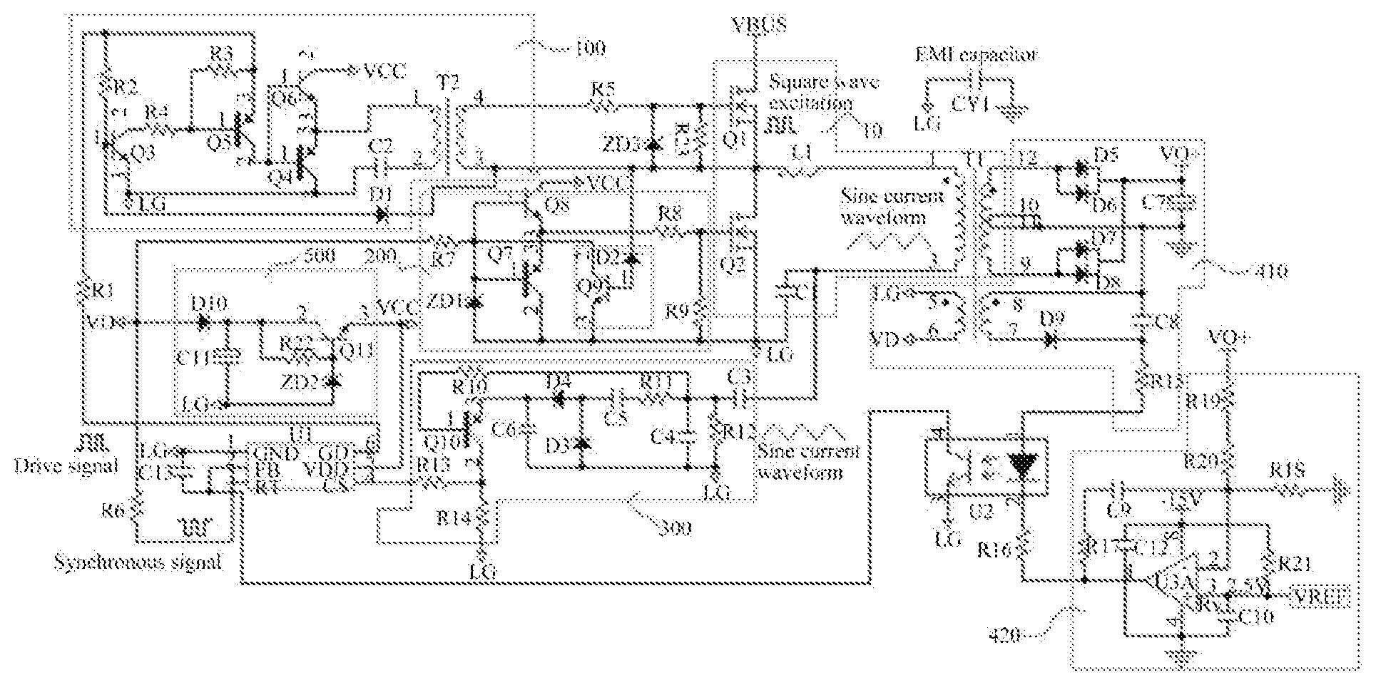
Referring to , this embodiment provides an LLC resonant topology control circuit based on a flyback chip, including an LLC resonant cavity 10 , a current mode flyback chip U 1 , a first drive circuit 100 , a second drive circuit 200 , a charge pump circuit 300 and a feedback circuit. The LLC resonant cavity includes a switching transistor Q 1 , a switching transistor Q 2 , a resonant inductor L 1 , a resonant capacitor C 1 and an output transformer T 1 ; a drain of the switching transistor Q 1 is connected to a VBUS end of a power supply; a source of the switching transistor Q 1 is connected with a drain of the switching transistor Q 2 and one end of the resonant inductor L 1 respectively; the other end of the resonant inductor L 1 is connected with one end of the resonant capacitor C 1 through a primary coil of the output transformer T 1 , and the other end of the resonant capacitor C 1 and a source of the switching transistor Q 2 are connected with an LG end of the power supply; a gate of the switching transistor Q 1 is connected with an output end of the first drive circuit 100 ; an input end of the first drive circuit 100 is connected with a GD end of the current mode flyback chip U 1 ; a gate of the switching transistor Q 2 is connected with an output end of the second drive circuit 200 ; an input end of the second drive circuit 200 is connected with an RT end of the current mode flyback chip U 1 ; one end of the resonant capacitor C 1 is connected with a CS end of the current mode flyback chip U 1 through the charge pump circuit 300 ; a secondary coil of the output transformer T 1 is connected with an input end of the feedback circuit; and an output end of the feedback circuit is connected with an FB end of the current mode flyback chip U 1 through an optically coupled isolator U 2 . Specifically, the current mode flyback chip U 1 provided in this embodiment adopts an OB2263/8 series flyback chip.
In this embodiment, the first drive circuit 100 may include triodes Q 3 to Q 6 , a transformer T 2 , a diode D 1 , a capacitor C 2 and resistors R 2 to R 4 ; the GD end of the current mode flyback chip U 1 is connected with one end of the resistor R 2 , one end of the resistor R 3 and an emitter of the triode Q 5 through a resistor R 1 ; the other end of the resistor R 2 is connected with a base of the triode Q 3 and a positive pole of the diode D 1 respectively; a collector of the triode Q 3 is connected with the other end of the resistor R 3 and a base of the triode Q 5 respectively through the resistor R 4 ; a collector of the triode Q 5 is connected with a base of the triode Q 4 and a base of the triode Q 6 respectively; an emitter of the triode Q 6 is connected with an emitter of the triode Q 4 and one end of a primary coil of the transformer T 2 respectively; the other end of the primary coil of the transformer T 2 is connected with one end of the capacitor C 2 ; one end of a secondary coil of the transformer T 2 is connected with a gate of the switching transistor Q 1 through the resistor R 5 ; the other end of the secondary coil of the transformer T 2 is respectively connected with a negative pole of the diode D 1 and one end of the resonant inductor L 1 ; the other end of the capacitor C 2 , a collector of the triode Q 4 and an emitter of the triode Q 3 are all connected with the LG end of the power supply; and a collector of the triode Q 6 is connected with a VCC end of the power supply.
The second drive circuit 200 may include triodes Q 7 to Q 9 , a voltage stabilizing diode ZD 1 , a diode D 2 and resistors R 7 to R 9 ; the RT end of the current mode flyback chip U 1 is connected with one end of the resistor R 7 through the resistor R 6 ; the other end of the resistor R 7 is respectively connected with a base of the triode Q 7 , a base of the triode Q 8 , a collector of the triode Q 9 and a negative pole of the voltage stabilizing diode ZD 1 ; an emitter of the triode Q 8 is respectively connected with an emitter of the triode Q 7 and one end of the resistor R 8 ; a base of the triode Q 9 is connected with one end of the resonant inductor L 1 through the diode D 2 ; the other end of the resistor R 8 is connected with one end of the resistor R 9 and a gate of the switching transistor Q 2 ; the other end of the resistor R 9 , an emitter of the triode Q 9 , a collector of the triode Q 7 and a positive pole of the voltage stabilizing diode ZD 1 are all connected with the LG end of the power supply; and a collector of the triode Q 8 is connected with the VCC end of the power supply.
The charge pump circuit 300 may include a triode Q 10 , diodes D 3 to D 4 , capacitors C 3 to C 6 , and resistors R 10 to R 14 ; one end of the resonant capacitor C 1 is respectively connected with one end of the resistor R 10 , one end of the resistor R 11 , one end of the resistor R 12 and one end of the capacitor C 4 through the capacitor C 3 ; the other end of the resistor R 11 is respectively connected with a positive pole of the diode D 4 and a negative pole of the diode D 3 through the capacitor C 5 ; the negative pole of the diode D 4 is connected with one end of the capacitor C 6 and an emitter of the triode Q 10 ; a base of the triode Q 10 is connected with the other end of the resistor R 10 ; a collector of the triode Q 10 is connected with one end of the resistor R 13 and one end of the resistor R 14 ; the other end of the resistor R 13 is connected with the CS end of the current mode flyback chip U 1 ; and the other end of the resistor R 14 , the other end of the resistor R 12 , the other end of the capacitor C 4 , the positive pole of the diode D 3 and the other end of the capacitor C 6 are all connected with the LG end of the power supply.
The feedback circuit may include a rectifier power supply circuit 410 and a sampling circuit 420 . The rectifier power supply circuit 410 may include capacitors C 7 to C 8 , diodes D 5 to D 9 , and a resistor R 15 . One end of the secondary coil of the output transformer T 1 is connected with a positive pole of the diode D 5 and a positive pole of the diode D 6 ; the other end of the secondary coil of the output transformer T 1 is respectively connected with a positive pole of the diode D 7 and a positive pole of the diode D 8 ; an adjustment end of the secondary coil of the output transformer T 1 is connected with one end of the capacitor C 7 and one end of the capacitor C 8 ; the other end of the capacitor C 7 is respectively connected with a negative pole of the diode D 5 , a negative pole of the diode D 6 , a negative pole of the diode D 7 and one end of a negative pole of the diode D 8 ; the other end of the capacitor C 8 is connected with one input end of the optically coupled isolator U 2 through the resistor R 15 ; the sampling circuit 420 includes an operational amplifier U 3 A, capacitors C 9 to C 10 , and resistors R 17 to R 21 ; the other input end of the optically coupled isolator U 2 is connected with one end of the resistor R 17 and an output end of the operational amplifier U 3 A through the resistor R 16 ; the other end of the resistor R 17 is respectively connected with one end of the resistor R 18 , one end of the resistor R 20 and an inverting input end of the operational amplifier U 3 A through the capacitor C 9 ; the other end of the resistor R 20 is connected with the other end of the capacitor C 7 through the resistor R 19 ; a non-inverting input end of the operational amplifier U 3 A is connected with one end of the resistor R 21 and one end of the capacitor C 10 ; the other end of the resistor R 21 is connected with a +15V power end; and the other end of the capacitor C 10 and the other end of the resistor R 18 are grounded.
Further, the LLC resonant topology control circuit based on a flyback chip provided by this embodiment further includes a power circuit 500 . The power circuit 500 includes a triode Q 11 , a voltage stabilizing diode ZD 2 , a capacitor C 11 , a diode D 10 and a resistor R 22 ; an emitter of the triode Q 11 is the VCC end of the power supply; a base of the triode Q 11 is respectively connected with one end of the resistor R 22 and a negative pole of the voltage stabilizing diode ZD 2 ; the other end of the resistor R 22 is respectively connected with a collector of the triode Q 11 , one end of the capacitor C 11 and a negative pole of the diode D 10 ; a positive pole end of the diode D 10 is the VD end of the power supply; and the other end of the capacitor C 11 and a positive pole of the voltage stabilizing diode ZD 2 are jointly connected to one point which is the LG end of the power supply.
The LLC resonant topology control circuit based on a flyback chip provided by this embodiment includes the LLC resonant cavity 10 , the current mode flyback chip U 1 , the first drive circuit 100 , the second drive circuit 200 , the charge pump circuit 300 and the feedback circuit. The LLC resonant topology control circuit works synchronously at an operating frequency of a feedback circuit of the LLC resonant cavity 10 through the resistor R 6 by virtue of a frequency setting pin of the current mode flyback chip U 1 . The charge pump circuit 300 includes the triode Q 10 , the diodes D 3 to D 4 , the capacitors C 3 to C 6 and the resistors R 10 to R 14 to complete current-voltage conversion. The charge pump divides the current of the resonant capacitor C 1 via the capacitor C 3 . When the LLC resonant cavity 10 has much energy, the voltage of the resonant capacitor C 1 increases. The voltage of the diode D 3 /D 4 also increases after rectification and exceeds a protection threshold set by the CS end of the current mode flyback chip U 1 . Furthermore, if the voltage of the resonant capacitor C 1 in the LLC resonant cavity 10 decreases to be less than 0 and becomes negative, the triode Q 10 is turned on, and the CS end of the current mode flyback chip U 1 performs cycle by cycle overcurrent protection (OCP), thus triggering overpower protection. The power circuit 500 in this embodiment includes the triode Q 11 , the voltage stabilizing diode ZD 2 , the capacitor C 11 , the diode D 10 and the resistor R 22 , so as to form a voltage stabilizing circuit to supply power to the current mode flyback chip U 1 . The diode D 9 and the capacitor C 8 supply power to the feedback circuit. The feedback circuit composed of the operational amplifier U 3 A controls an output voltage of the current mode flyback chip U 1 through the optically coupled isolator U 2 .
An operation startup mechanism: The current mode flyback chip U 1 is powered on and sends a drive signal. After the drive signal passes through the resistor R 1 , the drive transformer T 2 is pushed by the triodes Q 4 and Q 6 to drive the switching transistor Q 1 in an upper bridge arm to be turned on. The LLC resonant cavity 10 starts to work. The VD is reversely biased and turned off. After the second half cycle, the VD is positive. The VD drives, through the resistor R 7 , the switching transistor Q 2 in a lower bridge arm to be turned on. The triode Q 3 and the diode D 1 , as well as the triode Q 9 and the diode D 2 , are self-locked to prevent direct connection between the switching transistors Q 1 and Q 2 in the resonant cavity.
The key of the LLC resonant topology control circuit based on a flyback chip provided by this embodiment is an operation startup and protection mechanism. For the startup, only the upper bridge arm is controlled. The lower bridge arm is self-excited and driven by the transformer T 2 . For the protection, the triode Q 3 and the diode D 1 , as well as the triode Q 9 and the diode D 2 , achieve interlocking of drive signals to prevent direct connection. The OCP in the LLC resonant cavity 10 is achieved by the triode Q 10 and the charge pump.
Compared with the traditional LLC resonant control circuit, the LLC resonant topology control circuit based on the flyback chip provided by this embodiment adopts the current mode flyback chip U 1 to control LLC resonant topology. The chip has a small volume, which is much smaller than the chip package of the existing market. Furthermore, the chip has lower cost and flexible design, and the product competitiveness can be effectively improved.
The technical features of the embodiments described above can be arbitrarily combined. In order to make the description concise, all possible combinations of various technical features in the above embodiments are not completely described. However, the combinations of these technical features should be considered as the scope described in this specification as long as there is no contradiction in them.
The above-mentioned embodiments only express several implementation modes of the present disclosure, and their descriptions are more specific and detailed, but they cannot be understood as limiting the patent scope of the present disclosure. It should be noted that those of ordinary skill in the art can further make various transformations and improvements without departing from the concept of the present disclosure, and these transformations and improvements all fall within the protection scope of the present disclosure. Therefore, the protection scope of the patent of the present disclosure shall be subject to the appended claims.
Figures (1)
Citations
This patent cites (8)
- US12133305
- US2008/0094047
- US2015/0171754
- US101039075
- US107769569
- US208015594
- US109547721
- US112671246