Lithography and Method of Fabricating Semiconductor Device Using the Same
Abstract
A method includes grouping, in a first layout, pattern regions which have duplicate layout patterns including weak regions as a group, calculating defect probabilities of the pattern regions, respectively, calculating a defect frequency and a defect rate of the group based on the defect probabilities of the pattern regions, predicting a degree of defects of a second layout of the pattern regions, based on the defect frequency and the defect rate, and performing an extreme ultraviolet (EUV) lithography process on a substrate, based on the second layout. The defect probabilities are calculated by performing an optical proximity correction (OPC) simulation on the pattern region, calculating a stochastic variation of a linewidth of a simulation pattern in the weak region as a Gaussian distribution, and defining a threshold linewidth, which is used as a reference of the random defect, in the Gaussian distribution.
Claims (20)
1. A method comprising: in a first layout, grouping pattern regions, which have duplicate layout patterns, as a group, each of the pattern regions comprising a weak region in which a random defect may occur when an extreme ultraviolet (EUV) lithography process is performed; for each of the pattern regions, performing an optical proximity correction (OPC) simulation on the pattern region, calculating a stochastic variation of a linewidth of a simulation pattern in the weak region as a Gaussian distribution, and defining a threshold linewidth, which is used as a reference of the random defect, in the Gaussian distribution; calculating defect probabilities of the pattern regions, respectively, based on the threshold linewidths of the respective pattern regions; calculating a defect frequency and a defect rate of the group based on the defect probabilities of the pattern regions; predicting a degree of defects of a second layout of the pattern regions, based on the defect frequency and the defect rate; and performing an EUV lithography process on a substrate, based on the second layout.
11. A method comprising: searching for a pattern region in a first layout that includes a weak region in which a random defect may occur when an extreme ultraviolet (EUV) lithography process is performed; performing an optical proximity correction (OPC) simulation on the pattern region; calculating a stochastic variation of a linewidth of a simulation pattern in the weak region as a Gaussian distribution; defining a threshold linewidth as a reference of the random defect; applying the threshold linewidth to the Gaussian distribution to calculate a defect probability of the pattern region, based on the threshold linewidth; searching for the pattern region in a second layout to predict a degree of defects of the second layout; and performing an EUV lithography process on a substrate, based on the second layout.
16. A method comprising: in a first layout, grouping first pattern regions which have duplicate first layout patterns as a first group and grouping second pattern regions which have duplicate second layout patterns as a second group, the duplicate second layout patterns being different from the duplicate first layout patterns; calculating first defect probabilities of the first pattern regions, respectively; calculating second defect probabilities of the second pattern regions, respectively; calculating a first defect frequency and a first defect rate of the first group using the first defect probabilities; calculating a second defect frequency and a second defect rate of the second group using the second defect probabilities; and predicting defects in an extreme ultraviolet (EUV) lithography process based on the first defect frequency, the first defect rate, the second defect frequency, and the second defect rate.
Show 17 dependent claims
2. The method of claim 1 , wherein the calculating of the stochastic variation of the linewidth comprises: calculating Gaussian distributions of contours of the simulation pattern in the weak region; and summing the Gaussian distributions of the contours.
3. The method of claim 2 , wherein the contours comprise a first edge and a second edge, the calculating of the Gaussian distributions of the contours comprises: calculating a first stochastic variation of the first edge as a first Gaussian distribution; and calculating a second stochastic variation of the second edge as a second Gaussian distribution, and the summing the Gaussian distributions of the contours comprises summing the first Gaussian distribution and the second Gaussian distribution.
4. The method of claim 3 , wherein a first standard deviation of the first Gaussian distribution is different from a second standard deviation of the second Gaussian distribution.
5. The method of claim 1 , wherein the defect frequency is a sum of the defect probabilities of the pattern regions of the group, and the defect rate is a value that is obtained by dividing the defect frequency by a number of the pattern regions in the group.
6. The method of claim 1 , wherein the defect probabilities of the pattern regions of the group have values that are different from each other.
7. The method of claim 1 , wherein the pattern regions comprises a first pattern region at a first position on the first layout and a second pattern region at a second position on the first layout, the first pattern region and the second pattern region have a same shape, and a first standard deviation of the Gaussian distribution calculated from the first pattern region is different from a second standard deviation of the Gaussian distribution calculated from the second pattern region.
8. The method of claim 1 , wherein the first layout is a virtual layout that is generated based on a virtual netlist, and the second layout is a layout of a semiconductor device.
9. The method of claim 1 , further comprising modifying a layout pattern of the second layout, based on a predicted defect of the second layout.
10. The method of claim 1 , further comprising determining whether a defect of a pattern, which is formed on the substrate by the EUV lithography process, corresponds to the random defect, based on a predicted defect of the second layout.
12. The method of claim 11 , wherein the simulation pattern in the weak region comprises a first edge and a second edge, and the calculating of the stochastic variation of the linewidth comprises: calculating a first stochastic variation of the first edge as a first Gaussian distribution; calculating a second stochastic variation of the second edge as a second Gaussian distribution; and summing the first Gaussian distribution and the second Gaussian distribution as the Gaussian distribution.
13. The method of claim 12 , wherein the linewidth is a distance between the first edge and the second edge.
14. The method of claim 12 , wherein a first standard deviation of the first Gaussian distribution is different from a second standard deviation of the second Gaussian distribution.
15. The method of claim 12 , wherein the calculating of the first stochastic variation of the first edge comprises using a stochastic variation band (SVB) of the first edge, the SVB decreases as an intensity value of an EUV light increases, and the SVB decreases as an EUV sensitivity value increases.
17. The method of claim 16 , wherein each of the first pattern regions comprises a weak region in which a random defect may occur when an extreme ultraviolet (EUV) lithography process is performed, and the calculating of the first defect probabilities comprises, for each first pattern region: performing an OPC simulation on the first pattern region; calculating a stochastic variation of a linewidth of a simulation pattern in the weak region as a Gaussian distribution; and defining a threshold linewidth as a reference of the random defect, in the Gaussian distribution, wherein the first defect probabilities are calculated based on the threshold linewidth.
18. The method of claim 16 , wherein the first defect frequency is a sum of the first defect probabilities of the first pattern regions of the first group, and the first defect rate is a value that is obtained by dividing the first defect frequency by a number of the first pattern regions in the first group.
19. The method of claim 16 , wherein the second defect frequency is a sum of the second defect probabilities of the second pattern regions of the second group, and the second defect rate is a value that is obtained by dividing the second defect frequency by a number of the second pattern regions in the second group.
20. The method of claim 16 , wherein the first defect frequency is higher than the second defect frequency, and the first defect rate is lower than the second defect rate.
Full Description
Show full text →
CROSS-REFERENCE TO RELATED APPLICATIONS
This U.S. non-provisional patent application claims priority under 35 U. S. C. § 119 to Korean Patent Application No. 10-2021-0109909, filed on Aug. 20, 2021, in the Korean Intellectual Property Office, the entire contents of which are hereby incorporated by reference.
BACKGROUND OF THE INVENTION
The present disclosure relates to a method of fabricating a semiconductor device using a method of predicting defects in an EUV lithography process.
Due to their small-sized, multifunctional, and/or low-cost characteristics, semiconductor devices are being esteemed as important elements in the electronics industry. The semiconductor devices are classified into a semiconductor memory device for storing data, a semiconductor logic device for processing data, and a hybrid semiconductor device including both of memory and logic elements. As the electronic industry advances, there is an increasing demand for semiconductor devices with improved characteristics. For example, there is an increasing demand for semiconductor devices with high reliability, high performance, and/or multiple functions. To meet this demand, structural complexity and/or integration density of semiconductor devices are being increased.
SUMMARY
It is an aspect to provide a method of improving reliability in an EUV lithography process, which is performed to fabricate a semiconductor device.
According to an aspect of one or more embodiments, a method may include, in a first layout, grouping pattern regions, which have duplicate layout patterns, as a group, each of the pattern regions comprising a weak region in which a random defect may occur when an extreme ultraviolet (EUV) lithography process is performed; calculating defect probabilities of the pattern regions, respectively; calculating a defect frequency and a defect rate of the group based on the defect probabilities of the pattern regions; predicting a degree of defects of a second layout of the pattern regions, based on the defect frequency and the defect rate; and performing an EUV lithography process on a substrate, based on the second layout. The calculating of the defect probabilities comprises, for each pattern region, performing an optical proximity correction (OPC) simulation on the pattern region; calculating a stochastic variation of a linewidth of a simulation pattern in the weak region as a Gaussian distribution; and defining a threshold linewidth, which is used as a reference of the random defect, in the Gaussian distribution.
According to another aspect of one or more embodiments, a method may include searching for a pattern region in a first layout that includes a weak region in which a random defect may occur when an extreme ultraviolet (EUV) lithography process is performed; performing an optical proximity correction (OPC) simulation on the pattern region; calculating a stochastic variation of a linewidth of a simulation pattern in the weak region as a Gaussian distribution; defining a threshold linewidth as a reference of the random defect; applying the threshold linewidth to the Gaussian distribution to calculate a defect probability of the pattern region; searching for the pattern region in a second layout to predict a degree of defects of the second layout; and performing an EUV lithography process on a substrate, based on the second layout.
According to yet another aspect of one or more embodiments, a method may include, in a first layout, grouping first pattern regions which have duplicate first layout patterns as a first group and grouping second pattern regions which have duplicate second layout patterns as a second group, the duplicate second layout patterns being different from the duplicate first layout patterns; calculating first defect probabilities of the first pattern regions, respectively; calculating second defect probabilities of the second pattern regions, respectively; calculating a first defect frequency and a first defect rate of the first group using the first defect probabilities; calculating a second defect frequency and a second defect rate of the second group using the second defect probabilities; and predicting defects in an extreme ultraviolet (EUV) lithography process based on the first defect frequency, the first defect rate, the second defect frequency, and the second defect rate.
BRIEF DESCRIPTION OF THE DRAWINGS
is a block diagram illustrating a computer system for performing a semiconductor design process, according to an embodiment;
is a flow chart illustrating a method of designing and fabricating a semiconductor device, according to an embodiment;
is a conceptual diagram illustrating a photolithography system using a photomask according to an embodiment;
is a flow chart illustrating a method of designing a semiconductor device according to an embodiment;
to 11 are diagrams illustrating the method of according to an embodiment;
are layout diagrams illustrating a method of designing a semiconductor device according to an embodiment;
is a plan view illustrating a semiconductor device according to an embodiment;
A to 15 D are sectional views, which are respectively taken along lines A-A′, B-B′, C-C′, and D-D′ of ;
A to 16 D are sectional views which are respectively taken along the lines A-A′, B-B′, C-C′, and D-D′ of to illustrate a semiconductor device according to an embodiment;
is a plan view illustrating a semiconductor device according to an embodiment.
DETAILED DESCRIPTION
Various example embodiments will now be described more fully with reference to the accompanying drawings, in which example embodiments are shown.
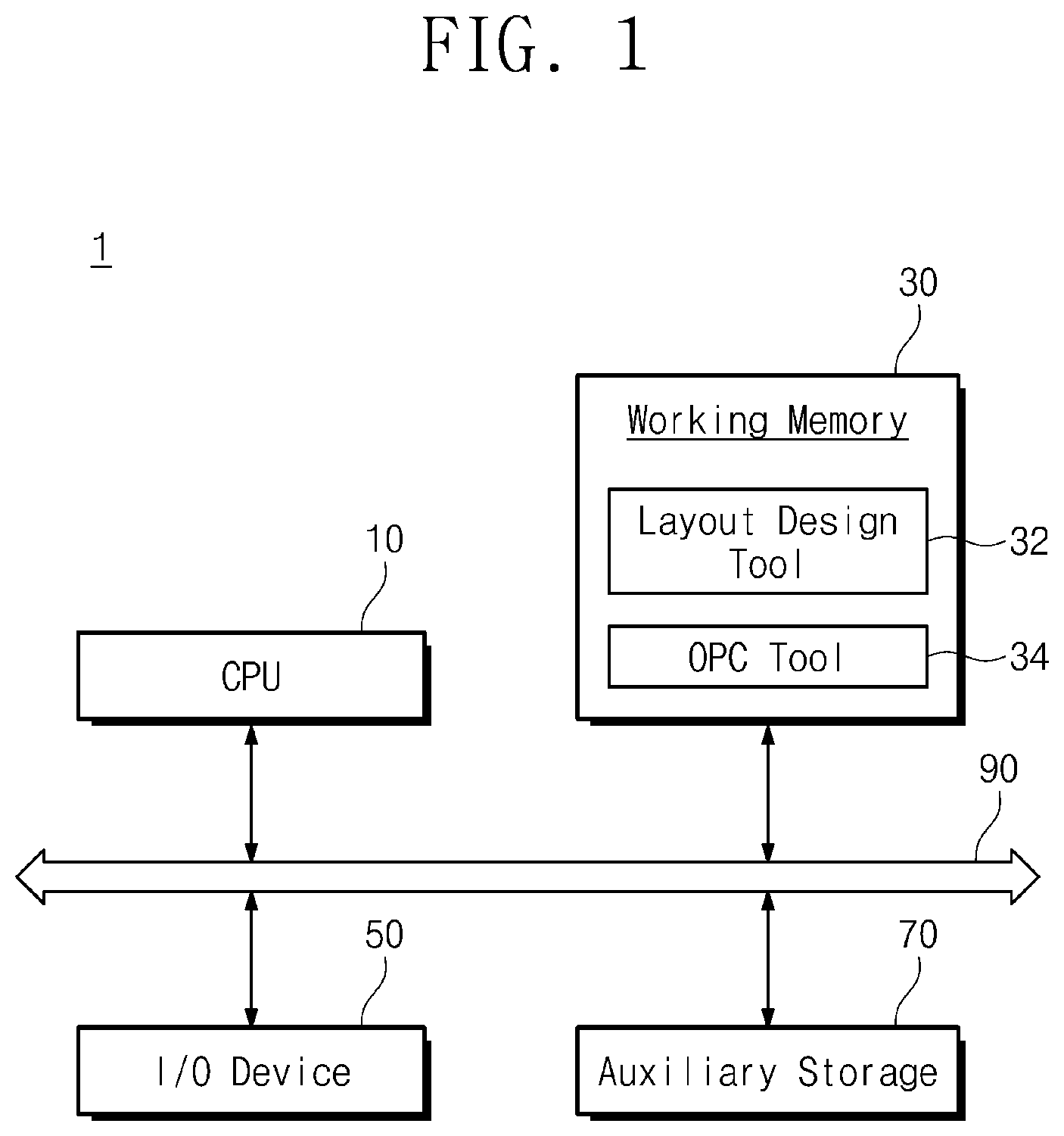
is a block diagram illustrating a computer system for performing a semiconductor design process, according to an embodiment. Referring to , a computer system 1 may include a central processing unit (CPU) 10 , a working memory 30 , an input-output (I/O) device 50 , and an auxiliary storage 70 . In an embodiment, the computer system 1 may be a system which is customized to perform a layout design process according to various embodiments. Furthermore, the computer system 1 may be configured to include various design and check simulation programs.
The CPU 10 may be configured to run a variety of software programs, such as application programs, operating systems, and device drivers, which will be executed in the computer system. For example, the CPU 10 may be configured to run an operating system (OS) (not shown) loaded in the working memory 30 . Furthermore, the CPU 10 may be configured to run various application programs, which will be executed on the operating system (OS). For example, the CPU 10 may be configured to run a layout design tool 32 and/or an optical proximity correction (OPC) tool 34 loaded in the working memory 30 .
The operating system or application programs may be loaded in the working memory 30 . For example, when the computer system starts a booting operation, an image (not shown) of the operating system stored in the auxiliary storage 70 may be loaded in the working memory 30 based on a booting sequence. Overall input/output operations of the computer system may be managed by the operating system (OS). An application program, which is chosen by a user or is provided for basic services, may be loaded in the working memory 30 . For example, the layout design tool 32 and/or the OPC tool 34 may be loaded in the working memory 30 from the auxiliary storage 70 .
The layout design tool 32 may provide a biasing function capable of changing shapes and positions of specific layout patterns to be different from those defined by a design rule. The layout design tool 32 may be configured to perform a design rule check (DRC) under the changed condition for the bias data. The OPC tool 34 may be configured to perform an optical proximity correction (OPC) process on layout data, which is output from the layout design tool 32 . The working memory 30 may be one of volatile memory devices (e.g., static random access memory (SRAM) or dynamic random access memory (DRAM) devices) or nonvolatile memory devices (e.g., PRAM, MRAM, ReRAM, FRAM, NOR FLASH memory devices), or the like.
The input-output (I/O) device 50 may be configured to control data to be input and output through a user interface device. For example, the input-output device 50 may include a keyboard or a monitor which is used to receive relevant information from a designer. By using the input-output device 50 , it may be possible for the designer to receive information on semiconductor regions or data paths requiring adjusted operating characteristics. The input-output device 50 may be configured to display a progressive status or result of a process that is executed by the OPC tool 34 .
The auxiliary storage 70 may be provided as a storage medium of the computer system 1 . The auxiliary storage 70 may be used to store the application programs, the image of the operating system, and various kinds of data. The auxiliary storage 70 may include one of memory cards (e.g., MMC, eMMC, SD, MicroSD, and so forth), a hard disk drive (HDD), or a solid state drive (SSD). In an embodiment, the auxiliary storage 70 may include a NAND FLASH memory device with a large memory capacity. In an embodiment, the auxiliary storage 70 may include next-generation non-volatile memory devices (e.g., PRAM, MRAM, ReRAM, and FRAM devices) or a NOR FLASH memory device, or the like.
A system interconnector 90 may be a system bus provided for an internal network of the computer system. The CPU 10 , the working memory 30 , the input-output device 50 , and the auxiliary storage 70 may be electrically connected to each other through the system interconnector 90 to exchange data with each other. However, the structure of the system interconnector 90 is not limited to this example and, in some embodiments, the system interconnector 90 may further include an interconnection element provided for efficient management.
is a flow chart illustrating a method of designing and fabricating a semiconductor device, according to an embodiment. Referring to , a high-level description process may be performed (in S 10 ). A high-level design of a semiconductor integrated circuit may be performed using the computer system 1 described with reference to . For example, in the high-level description process, an integrated circuit to be designed may be described with high-level computer language. An example of the high-level computer language may be a C language. Circuits designed by the high-level design process may be more concretely described by a register-transfer-level (RTL) coding or a simulation. Furthermore, codes generated by the RTL coding may be converted into a netlist and may be combined to describe the entirety of the semiconductor device. The combined schematic circuit may be verified by a simulation tool, and an adjusting step may be further performed based on a result of the verification step.
A layout design process may be performed (in S 20 ). The layout design process may be performed to realize the semiconductor integrated circuit of a logically complete form on a silicon wafer. For example, the layout design process may be performed, based on the schematic circuit prepared in the high-level description process or the corresponding netlist. The layout design process may include a routing step of placing and connecting various standard cells that are provided from a cell library, based on a design rule. The design rule may be predetermined.
The cell library for the layout design process may contain information on operation, speed, and power consumption of standard cells. In an embodiment, a cell library for representing a circuit of a specific gate level as a layout may be defined in the layout design tool. Here, the layout may be prepared to define shapes, positions, or sizes of patterns constituting transistors and metal lines, which will be actually formed on a silicon wafer. For example, in order to actually form an inverter circuit on a silicon wafer, layout patterns (e.g., PMOS, NMOS, N-WELL, gate electrodes, and metal lines thereon) may be appropriately placed. For this placement, at least one of inverters, which were previously defined in the cell library, may be searched and chosen.
The routing step may be performed on the chosen and placed standard cells. In detail, the routing step may be performed to connect the chosen and placed standard cells to upper-level lines. As a result of the routing step, the standard cells may be connected to each other in a designed manner. In an embodiment, the afore-described steps may be automatically or manually performed by the layout design tool 32 . In an embodiment, a step of placing and routing the standard cells may be performed using an additional Place & Routing tool.
After the routing step, a verification step may be performed on the layout to check whether there is a portion violating the design rule. In an embodiment, the verification step may include evaluating verification items, such as a design rule check (DRC), an electrical rule check (ERC), and a layout vs schematic (LVS) check. The evaluating of the DRC item may be performed to evaluate whether the layout meets the design rule. The evaluating of the ERC item may be performed to evaluate whether there is an issue of electrical disconnection in the layout. The evaluating of the LVS item may be performed to evaluate whether the layout is prepared to coincide with the gate-level netlist.
An optical proximity correction (OPC) process may be performed (in S 30 ) using an OPC technology. Layout patterns, which are prepared by the layout design process, may be realized on a silicon wafer through a photolithography process. The OPC process may be performed to correct an optical proximity or distortion effect, which may occur in the photolithography process. That is, by performing the OPC process, it may be possible to correct optical effects (e.g., refraction) or process effects, which may occur in an exposure step using a designed pattern. As a result of the OPC process, the shapes and positions of patterns in the designed layout may be changed or biased. The OPC process may be performed using the OPC tool 34 . The OPC process will be described in more detail with reference to .
A mask may be generated (in S 40 ). In more detail, a photomask may be manufactured, based on the layout modified by the OPC process (in S 40 ). In general, the photomask may be manufactured by patterning a chromium layer, which is formed on a glass substrate, to describe the layout patterns.
A semiconductor device may be manufactured (in S 50 ). In more detail, the manufactured photomask may be used to manufacture a semiconductor device. In the actual fabricating process using the photomask, various exposing and etching steps may be performed or repeated. As a result of the various exposing and etching steps, patterns, which are defined in the layout design process, may be sequentially formed on a silicon wafer.
is a conceptual diagram illustrating a photolithography system using a photomask according to an embodiment. In detail, illustrates an example of an extreme ultraviolet (EUV) lithography system 1000 .
In an embodiment, EUV light may have a wavelength of about 4 nm to about 124 nm (in particular, of about 4 nm to about 20 nm) and may be, for example, an ultraviolet light having a wavelength of 13.5 nm. The EUV light may have an energy of about 6.21 eV to about 124 eV (in particular, of about 90 eV to about 95 eV).
In general, an amount of photons per unit volume in the EUV light may be much smaller than that in the conventional KrF or ArF light. Since, for the EUV light, an intensity of a single photon is high but an amount of photons is small, at least a portion of an EUV resist layer on a wafer may not sufficiently react with the EUV light. Such a process defect may randomly occur during the EUV lithography process.
Referring to , the EUV lithography system 1000 may include a beam shaping system 1100 , an illumination system 1200 , a photomask 1300 , and a projection system 1400 . The beam shaping system 1100 , the illumination system 1200 , and the projection system 1400 may be disposed in respective housings. In an embodiment, the entirety or portion of the beam shaping system 1100 may be incorporated into the illumination system 1200 .
The beam shaping system 1100 may include a light source 1110 , a collector 1120 , and a monochromator 1130 . The light source 1110 may be a laser plasma source, a gas discharging source, or a synchrotron-based radiation source. Light, which is generated by the light source 1110 , may have a wavelength range of about 5 nm to about 20 nm. The illumination system 1200 and the projection system 1400 may be configured to be operated within the wavelength range. EUV light, which is emitted from the light source 1110 , may be focused by the collector 1120 . The monochromator 1130 may be configured to filter out unwanted wavelengths of light.
The EUV light whose wavelength and spatial distribution are adjusted in the beam shaping system 1100 may be incident into the illumination system 1200 . illustrates an example in which the illumination system 1200 includes two mirrors 1210 and 1220 . However, the number of the mirrors 1210 and 1220 is not limited to the number of mirrors illustrated in the example of and, in some embodiments, the number of mirrors may be more or less than two. Each of the mirrors 1210 and 1220 may be a multilayer mirror.
Due to the mirrors 1210 and 1220 in the illumination system 1200 , the EUV light may be incident into the photomask 1300 . The photomask 1300 may include image patterns, which are used to print or realize a designed layout on a substrate 100 . The image patterns may be formed, based on layout patterns prepared through the layout design and optical proximity correction processes described above. The image patterns may be defined by a reflection region reflecting the EUV light and an absorption region absorbing the EUV light. More specifically, the image patterns may include absorption patterns, which are formed on a reflection layer of the photomask 1300 . The absorption patterns may be formed of or include at least one of metal compounds (e.g., TaN, TaBN, or TaBON) which absorb but do not reflect the EUV light.
The incident EUV light may be reflected by the photomask 1300 . The reflected portion of the EUV light may be projected onto the substrate 100 , which is coated with a photoresist composite, through the projection system 1400 . The projection system 1400 may be configured to irradiate the EUV light, which is reflected by the photomask 1300 , onto the substrate 100 coated with the photoresist composite. A patterned structure may be imaged in the photoresist composite by the EUV irradiated onto the substrate 100 . illustrates an example in which the projection system 1400 includes two mirrors 1410 and 1420 . However, similar to the illumination system 1200 described above, the number of the mirrors 1410 and 1420 is not limited to the number of mirrors illustrated in the example of and, in some embodiments, the number of mirrors may be more or less than two. Each of the mirrors 1410 and 1420 may have a multilayer mirror.
As an integration density of a semiconductor device increases, a distance between the image patterns of the photomask 1300 may be reduced, thereby causing a proximity issue such as undesired interference and diffraction. As a result of the proximity issue, the photoresist patterns formed on the substrate 100 may have distorted shapes (i.e., different from those of the image patterns of the photomask 1300 ). The distortion of the photoresist patterns may lead to a malfunction of an electronic device or circuit that is formed on the substrate 100 .
A resolution enhancement technology may be used to prevent the distortion of the photoresist patterns. The optical proximity correction (OPC) technology, which is used in the step S 30 of , may be an example of the resolution enhancement technology. According to the OPC technology, the optical distortion issue, which is caused by interference and diffraction, may be predicted prior to forming the electronic device or circuit on the substrate 100 by a simulation process using an OPC model. The designed layout may be corrected or biased, based on the predicted result. Based on the corrected layout, photoresist patterns may be formed on the photomask 1300 , and therefore, the photoresist patterns may be formed in desired shapes on the substrate 100 .
A layout of a semiconductor device may include a plurality of layers. In an embodiment, the OPC step (i.e., S 30 in ) may be performed to correct a layout for each of the layers. That is, the OPC step may be independently performed on each of the plurality of layers. A semiconductor device may be fabricated by realizing the plurality of layers on a substrate through a semiconductor process. As an example, a semiconductor device may include a plurality of metal layers, which are stacked to realize a specific circuit.
is a flow chart illustrating a method of designing a semiconductor device according to an embodiment. to 10 are diagrams illustrating the method of according to an embodiment. illustrates a method of predicting defects in an EUV lithography process. More specifically, relates to a method of numerically representing by numerical data a defect frequency and a defect rate on each of unique pattern groups and predicting a degree of defects in an actual layout based on the numerical data.
Referring to with additional reference to , a first layout VLO may be provided. In an embodiment, the first layout VLO may be a virtual layout, which is generated based on a virtual netlist. The virtual netlist may be created by reducing an actual netlist. The virtual netlist may include a schematic circuit.
In another embodiment, the first layout VLO may be a layout of a semiconductor device that is currently fabricated or is in a mass production stage. That is, the first layout VLO may be a layout used in the past or used in a current fabrication process.
In an embodiment, the first layout VLO may be a layout that represents one of metal or interconnection layers to be formed through a back-end-of-line (BEOL) process. For example, the first layout VLO may be a layout representing one of a first metal layer M 1 , a second metal layer M 2 , a third metal layer M 3 , and additional metal layers (M 4 , M 5 , M 6 , . . . , Mn) thereon.
The first layout VLO may include a plurality of layout patterns LPT. The layout patterns LPT may correspond to interconnection lines, respectively, which are provided in a metal layer corresponding to the first layout VLO. The layout patterns LPT may be line-shaped patterns extending in a specific direction. As an example, the layout patterns LPT may be line-and-space patterns.
Referring now to , pattern regions, which are duplicate in the first layout VLO, may be grouped (in S 101 of ). That is, in the first layout VLO, pattern regions, which have a same layout pattern, may be grouped together in a group. For example, in a region where ends of the layout patterns LPT are located, there may be a unique shape that is composed of the layout patterns LPT. The region with the unique shape may be defined as a pattern region or a unique pattern region.
In an embodiment, the first layout VLO of may include a first pattern region DPR 1 , a second pattern region DPR 2 , a third pattern region DPR 3 , and a fourth pattern region DPR 4 . Each of the first to fourth pattern regions DPR 1 -DP 4 may include a plurality of duplicate regions in the first layout VLO.
For example, the first pattern region DPR 1 may include a plurality of first pattern regions DPR 1 having a same shape. In other words, a configuration of the layout patterns LPT may be the same within the first pattern regions DPR 1 . In detail, the duplicate first pattern regions DPR 1 may include the first pattern region DPR 1 located at a position A (DPR 1 (A)), the first pattern region DPR 1 located at a position B (DPR 1 (B)), and the first pattern region DPR 1 located at a position C (DPR 1 (C)). The three first pattern regions DPR 1 located at different positions may be grouped as a first group.
The second pattern region DPR 2 may include two second pattern regions DPR 2 located at different positions. The second pattern regions DPR 2 may be grouped as a second group. The third pattern region DPR 3 may include two third pattern regions DPR 3 located at different positions. The third pattern regions DPR 3 may be grouped as a third group. The fourth pattern region DPR 4 may include three fourth pattern regions DPR 4 located at different positions. It is noted that the two fourth pattern regions DPR 4 in the lower right of have a same shape but are symmetrical about a horizontal line. The groupings may include such symmetrically same pattern regions. The fourth pattern regions DPR 4 may be grouped as a fourth group.
An OPC simulation may be performed on the pattern region of each of the first to fourth groups (in S 102 of ). Hereinafter, the first group of the first pattern region DPR 1 will be described as a representative example. In an embodiment, the OPC simulation may be performed using the OPC tool 34 of .
Referring to , the first pattern region DPR 1 may include a first layout pattern LPT 1 , a second layout pattern LPT 2 , a third layout pattern LPT 3 , a fourth layout pattern LPT 4 , and a fifth layout pattern LPT 5 . The first and fourth layout patterns LPT 1 and LPT 4 may be spaced apart from each other in a specific direction. The first and fourth layout patterns LPT 1 and LPT 4 may be aligned to each other in the specific direction. The third and fifth layout patterns LPT 3 and LPT 5 may be spaced apart from each other in the specific direction. The third and fifth layout patterns LPT 3 and LPT 5 may be aligned to each other in the specific direction.
The second layout pattern LPT 2 may be provided between the first and third layout patterns LPT 1 and LPT 3 and between the fourth and fifth layout patterns LPT 4 and LPT 5 as illustrated in . The second layout pattern LPT 2 may have a line shape extending in the specific direction.
A weak region WER may be defined on the second layout pattern LPT 2 . The weak region WER may be located between ends of the first, third, fourth, and fifth layout patterns LPT 1 , LPT 3 , LPT 4 , and LPT 5 as illustrated in . The weak region WER may be a region, in which a random defect may occur when the EUV lithography process is performed on a wafer.
shows a process defect which may occur when the first to fifth layout patterns LPT 1 to LPT 5 are actually realized on the substrate 100 . Referring to , a target pattern TGP corresponding to the second layout pattern LPT 2 may not be formed in a line shape and may be divided into two portions spaced apart from each other. Since, for the EUV light in the EUV lithography process, an amount of photons per unit volume is small as described above, a single line open (SLO) defect, in which a line pattern is cut, may occur, as shown in . The SLO defect of may be a defect that occurs randomly. This random defect may occur in the weak region WER described above.
The random defect of may be a defect which is found not always but is found randomly in a stochastic aspect. Thus, according to an embodiment, it may be possible to quantitatively predict the random defect, which will occur when the unique pattern region is realized on an actual wafer, for each group.
Referring to A , the OPC simulation may be performed on the first pattern region DPR 1 to generate a first simulation pattern DIM 1 , a second simulation pattern DIM 2 , a third simulation pattern DIM 3 , a fourth simulation pattern DIM 4 , and a fifth simulation pattern DIM 5 corresponding to the first to fifth layout patterns LPT 1 to LPT 5 , respectively.
In detail, a first target pattern DTP 1 , a second target pattern DTP 2 , a third target pattern DTP 3 , a fourth target pattern DTP 4 , and a fifth target pattern DTP 5 may be respectively generated on the first to fifth layout patterns LPT 1 to LPT 5 . Each of the first to fifth target patterns DTP 1 to DTP 5 may be generated from a corresponding layout pattern through a table-driven layout operation (TDLO) step. Each of the first to fifth target patterns DTP 1 to DTP 5 may define a size of a pattern, which is developed from an EUV resist layer through the EUV lithography process. Each of the first to fifth target patterns DTP 1 to DTP 5 may denote a desired size of a photoresist pattern that is developed through the EUV lithography process. Each of the first to fifth target patterns DTP 1 to DTP 5 may have a size that is the same as or different from a correspond layout pattern.
The first to fifth simulation patterns DIM 1 to DIM 5 may be generated by performing an OPC process, which aims at the first to fifth target patterns DTP 1 to DTP 5 , on the first to fifth layout patterns LPT 1 to LPT 5 . For example, the first to fifth simulation patterns DIM 1 to DIM 5 may be generated to maximally correspond with the first to fifth target patterns DTP 1 to DTP 5 , respectively.
In the weak region WER, a contour of the second simulation pattern DIM 2 may include a first edge ED 1 and a second edge ED 2 which are opposite to each other. The first and second edges ED 1 and ED 2 of A may have a linear shape. However, as described above, a shape of a pattern in the weak region WER may be randomly deformed, due to a limitation in the EUV lithography process. In an ultimate deformation case, the defect shown in may occur in the weak region WER. That is, there may be a non-vanishing probability that the contour of the second simulation pattern DIM 2 in the weak region WER has a shape different from that of A .
Referring to B , the first and second edges ED 1 and ED 2 may have a shape that is recessed toward a center of the second simulation pattern DIM 2 . Referring to C , the first and second edges ED 1 and ED 2 may have a shape that is convex in a direction away from the center of the second simulation pattern DIM 2 . When A is chosen as a reference, there may be a non-vanishing probability that each of the first and second edges ED 1 and ED 2 has the deviation or displacement shown B or C .
Referring to , a variation of the contour of the second simulation pattern DIM 2 in the weak region WER may be calculated as Gaussian distributions (in S 103 of ). In detail, a stochastic variation related to a deviation of the first edge ED 1 may obey a first Gaussian distribution GD 1 whose center is located at a first reference edge ED 1 _R of A . The first edge ED 1 may be located at the first reference edge ED 1 _R with the highest probability. The first edge ED 1 may be located at a first positive edge ED 1 _A, which has a first deviation DIP 1 from the first reference edge ED 1 _R, with a lowered probability. The first edge ED 1 may be located at a first negative edge ED 1 _B, which has a minus value of the first deviation (i.e., -DIP 1 ) from the first reference edge ED 1 _R, with a lowered probability. The deviations DIP and -DIP 1 may be the standard deviation of the first Gaussian distribution GD 1 . In other words, the first edge ED 1 may have a stochastic variation band (SVB) in accordance with the first Gaussian distribution GD 1 .
The second edge ED 2 may also have a stochastic variation band in a similar manner as the first edge ED 1 described above. In detail, the second edge ED 2 may have a stochastic variation band in accordance with a second Gaussian distribution GD 2 . In other words, the second edge ED 2 may be located at a second reference edge ED 2 _R of A with the highest probability. The second edge ED 2 may be located at a second positive edge ED 2 _A, which has a second deviation DIP 2 from the second reference edge ED 2 _R, with a lowered probability. The second edge ED 2 may be located at a second negative edge ED 2 _B, which has a minus value of the second deviation (i.e., -DIP 2 ) from the second reference edge ED 2 _R, with a lowered probability.
As shown in , a contour in the weak region WER (i.e., each of the first and second edges ED 1 and ED 2 ) may not be fixed to a specific reference shape ED 1 _R or ED 2 _R but may vary stochastically.
According to an embodiment, the stochastic variation to the contour in the weak region WER described above may be calculated as a Gaussian distribution. The Gaussian distribution of the contour (i.e., the stochastic variation band (SVB)) may be calculated based on the following DMS model: SVB=a*(DMS) n +b
where SVB denotes the stochastic variation band, DMS denotes a dose mask sensitivity, “n” denotes an experimentally determined constant, and “a” and “b” denote optimized values in a regression analysis. The dose mark sensitivity (DMS) is represented by the following expression:
DMS = f ( MEEF ) I m a x * ILS
The dose mask sensitivity (DMS) model may represent a stochastic variation of the contour in the weak region WER in terms of an EUV dose and a photomask factor. The DMS may be proportional to the photomask factor (f(MEEF)). The DMS may be inversely proportional to an intensity (Imax) of the EUV light and sensitivity (i.e., image log-slope (ILS)) in the EUV process. The sensitivity (ILS) may mean a change ratio of a light intensity at a boundary between an exposed region and an unexposed region in the EUV lithography process.
The higher the values of Imax and ILS, the smaller the value of the DMS and the stochastic variation of the contour. In other words, the DMS may indicate an accuracy in the EUV lithography process. That is, the smaller the value of the DMS, the smaller the variation of the contour ED 1 or ED 2 shown in . The smaller the value of the DMS, the smaller the standard deviation of the Gaussian distribution GD 1 or GD 2 . The standard deviation DIP 1 of the first Gaussian distribution GD 1 of may be smaller than the standard deviation DIP 2 of the second Gaussian distribution GD 2 . For example, the DMS value of the first edge ED 1 of may be smaller than the DMS value of the second edge ED 2 . In the case where the value of the DMS is small, a defect probability in the weak region WER may be lowered. The first or second Gaussian distribution GD 1 or GD 2 of (i.e., SVB) for each contour may be calculated, based on the afore-described DMS model.
Referring to , a single Gaussian distribution for a stochastic variation of a linewidth of a pattern may be calculated by summing the Gaussian distributions of the contour in the weak region WER (in S 104 of ). In detail, a third Gaussian distribution GD 3 , which represents a stochastic variation of a linewidth of a pattern (e.g., the second simulation pattern DIM 2 ), may be calculated by summing the first and second Gaussian distributions GD 1 and GD 2 of the first and second edged ED 1 and ED 2 of .
A pattern on the weak region WER (i.e., the second simulation pattern DIM 2 ) may have a reference linewidth LW_R. Since each of the first and second edges ED 1 and ED 2 varies stochastically, a linewidth of the second simulation pattern DIM 2 may also vary stochastically.
For example, the linewidth of the second simulation pattern DIM 2 may have the reference linewidth LW_R, with the highest probability. The linewidth of the second simulation pattern DIM 2 may have a first linewidth LW_A, which has a third deviation from the reference linewidth LW_R, with a lowered probability. The linewidth of the second simulation pattern DIM 2 may have a second linewidth LW_B, which has a minus value of the third deviation from the reference linewidth LW_R, with a lowered probability. In other words, the linewidth of the second simulation pattern DIM 2 may have a stochastic variation band (i.e., SVB) in accordance with the third Gaussian distribution GD 3 .
A threshold linewidth LW_th, which is used as a defect reference in the third Gaussian distribution GD 3 , may be defined and then a defect probability may be calculated (in S 105 of ). In the case where a linewidth of a pattern on the weak region WER has a value that is smaller than a specific threshold value, a defect may occur, as shown in . Accordingly, the threshold linewidth LW_th, which is used as a reference of defect occurrence, may be defined. In an embodiment, the threshold linewidth LW_th may be defined or determined in consideration of whether the defect shown in occurs on an actual wafer when a linewidth of a pattern on the weak region WER is smaller than a specific value.
In the third Gaussian distribution GD 3 of , a defect probability DF_P may be calculated by obtaining an area of a graph of the third Gaussian distribution GD 3 to the threshold linewidth LW_th. That is, the defect probability DF_P of the first pattern region DPR 1 in the weak region WER may be calculated using the afore-described steps.
Even when, as shown in , the first pattern regions DPR 1 are provided to have the same shape at the position A, the position B, and the position C, the defect probability of the first pattern region DPR 1 may vary depending on the position A, B, or C. This variation may be because the intensity of the EUV light and the sensitivity in the EUV process vary depending on a position on a wafer. Accordingly, it may be advantageous to calculate the defect probabilities of the first pattern regions DPR 1 at the positions A, B, and C, respectively. That is, according to an embodiment, the defect probabilities may be calculated for pattern regions, which are located at different positions, in each group.
A defect frequency and a defect rate for each group may be calculated and collected, based on the defect probabilities of the pattern regions calculated by the afore-described methods (in S 106 of ).
In detail, referring to , the first pattern regions DPR 1 at the positions A, B, and C may have respective third Gaussian distributions GD 3 that are different from each other. The third Gaussian distribution GD 3 of the first pattern region DPR 1 at the position A (i.e., DPR 1 (A)), the third Gaussian distribution GD 3 of the first pattern region DPR 1 at the position B (i.e., DPR 1 (B)), and the third Gaussian distribution GD 3 of the first pattern region DPR 1 at the position C (i.e., DPR 1 (C)) may have different standard deviations from each other. In other words, a stochastic variation of a linewidth of a first pattern region DP 1 in the weak region WER may vary depending on position. Even when the same threshold linewidth LW_th is chosen as reference, the defect probabilities of the first pattern regions DPR 1 at the positions A, B, and C may be calculated as, for example, 0.25, 0.35, and 0.15, respectively.
The defect frequency of the first group of the first pattern regions DPR 1 may be a sum of the defect probabilities (i.e., 0.75=0.25+0.35+0.15). The defect rate may be a value that is obtained by dividing the defect frequency by the number of the pattern regions (i.e., 0.25=0.75/3). That is, on a wafer, the predicted number of the defects, which occur in association with the first pattern region DPR 1 , may be 0.75, and a mean defect probability of the first pattern region DPR 1 may be 0.25.
Next, the defect probability may also be calculated for the second pattern regions DPR 2 of the second group. For example, the defect probability of one of two second pattern regions DPR 2 may be 0.30, and the defect probability of the other may be 0.35. Here, the defect frequency of the second group may be 0.65, and the defect rate may be 0.325.
The defect frequency of the second group (i.e., 0 . 65 ) may be smaller than the defect frequency of the first group (i.e., 0 . 75 ). This difference may be because the number of the second pattern regions DPR 2 of the second group (i.e., two) is smaller than the number of the first pattern regions DPR 1 of the first group (i.e., three). However, it may be seen that the defect rate of the second group is greater than the defect rate of the first group. Only when both of the defect frequency and the defect rate are calculated for each group as described above may the occurrence of the defect may be predicted more accurately.
A degree of defects of the second layout may be predicted based on the defect frequency and the defect rate calculated or obtained for each groups by the above process (in S 107 of ). Unlike the first layout VLO of , the second layout may be an actual layout of a semiconductor device which will be produced in the future. Hereinafter, a method of applying information on the defect frequency and the defect rate of the unique patterns or groups to the second layout (i.e., the actual layout) will be described exemplarily.
are layout diagrams illustrating a method of designing a semiconductor device according to an embodiment.
Referring to , unique pattern regions in a second layout LO may be searched. A defect frequency and a defect rate of a group, in which the unique pattern regions are grouped, may be calculated and collected in advance through the afore-described method of . For example, the first pattern region DPR 1 of the first group may be searched in the second layout LO. This search process may be performed in consideration of a defect probability by a position of the first pattern region DPR 1 of and a defect frequency and a defect rate of the first group, in which the first pattern region DPR 1 is included.
Referring to , if a defect is predicted to occur in the first pattern region DPR 1 of with a high probability, the first pattern region DPR 1 of the second layout LO may be modified. For example, an end of each of the layout patterns LPT 1 , LPT 3 , LPT 4 , and LPT 5 may be modified or biased to lower an occurrence probability of the defect, as shown in .
is a plan view illustrating a semiconductor device according to an embodiment. A to 15 D are sectional views taken along lines A-A′, B-B′, C-C′, and D-D′, respectively, of . A to 15 D illustrate an example of a semiconductor device, in which the second layout LO of is realized as the second metal layer M 2 on a substrate.
Referring to A to 15 D , a logic cell may be provided on the substrate 100 . Logic transistors constituting a logic circuit may be disposed on the logic cell.
The substrate 100 may include a first active region PR and a second active region NR. In an embodiment, the first active region PR may be a PMOSFET region, and the second active region NR may be an NMOSFET region. The substrate 100 may be a semiconductor substrate including silicon, germanium, silicon germanium, or the like or a compound semiconductor substrate. In an embodiment, the substrate 100 may be a silicon wafer.
The first and second active regions PR and NR may be defined by a second trench TR 2 (see, e.g., C ), which is formed in an upper portion of the substrate 100 . The second trench TR 2 may be located between the first and second active regions PR and NR. The first and second active regions PR and NR may be spaced apart from each other, in a first direction D 1 , with the second trench TR 2 interposed therebetween. Each of the first and second active regions PR and NR may be extended in a second direction D 2 that is different from (e.g., perpendicular to) the first direction D 1 .
First active patterns AP 1 and second active patterns AP 2 may be provided on the first active region PR and the second active region NR, respectively. The first and second active patterns AP 1 and AP 2 may be extended in the second direction D 2 to be parallel to each other. Each of the first and second active patterns AP 1 and AP 2 may be a vertically-protruding portion (e.g., protruding in a third direction D 3 ) of the substrate 100 . A first trench TR 1 may be defined between adjacent ones of the first active patterns AP 1 and between adjacent ones of the second active patterns AP 2 . The first trench TR 1 may be shallower than the second trench TR 2 .
A device isolation layer ST may be provided to fill the first and second trenches TR 1 and TR 2 . The device isolation layer ST may include a silicon oxide layer. Upper portions of the first and second active patterns AP 1 and AP 2 may protrude vertically above the device isolation layer ST (e.g., see D ). Each of the upper portions of the first and second active patterns AP 1 and AP 2 may be a fin-shaped pattern. The device isolation layer ST may not cover the upper portions of the first and second active patterns AP 1 and AP 2 . The device isolation layer ST may cover lower side surfaces of the first and second active patterns AP 1 and AP 2 .
First source/drain patterns SD 1 may be provided in the upper portions of the first active patterns AP 1 (see, e.g., C ). The first source/drain patterns SD 1 may be impurity regions of a first conductivity type (e.g., p-type). A first channel pattern CH 1 may be interposed between each pair of the first source/drain patterns SD 1 (see, e.g., A ). Second source/drain patterns SD 2 may be provided in the upper portions of the second active patterns AP 2 (see, e.g., B ). The second source/drain patterns SD 2 may be impurity regions of a second conductivity type (e.g., n-type). A second channel pattern CH 2 may be interposed between each pair of the second source/drain patterns SD 2 .
The first and second source/drain patterns SD 1 and SD 2 may be epitaxial patterns, which are formed by a selective epitaxial growth process. In an embodiment, the first and second source/drain patterns SD 1 and SD 2 may have top surfaces that are coplanar with top surfaces of the first and second channel patterns CH 1 and CH 2 . Alternatively, in some example embodiments, the top surfaces of the first and second source/drain patterns SD 1 and SD 2 may be higher than the top surfaces of the first and second channel patterns CH 1 and CH 2 .
The first source/drain patterns SD 1 may be formed of or include a semiconductor material (e.g., SiGe) having a lattice constant greater than that of the substrate 100 . In this case, the first source/drain patterns SD 1 may exert a compressive stress on the first channel patterns CH 1 . The second source/drain patterns SD 2 may be formed of or include the same semiconductor material (e.g., Si) as the substrate 100 .
Gate electrodes GE may be provided to cross the first and second active patterns AP 1 and AP 2 and to extend in the first direction D 1 (see, e.g., A and 15 B ). The gate electrodes GE may be arranged at a constant pitch in the second direction D 2 . The gate electrodes GE may be vertically overlapped with the first and second channel patterns CH 1 and CH 2 . Each of the gate electrodes GE may be provided to face a top surface and opposite side surfaces of each of the first and second channel patterns CH 1 and CH 2 .
Referring to D , the gate electrode GE may be provided on a first top surface TS 1 of the first channel pattern CH 1 and on at least one first side surface SW 1 of the first channel pattern CH 1 . The gate electrode GE may be provided on a second top surface TS 2 of the second channel pattern CH 2 and on at least one second side surface SW 2 of the second channel pattern CH 2 . In other words, the transistor according to D may be a three-dimensional field-effect transistor (e.g., FinFET), in which the gate electrode GE is provided to three-dimensionally surround the first or second channel pattern CH 1 or CH 2 .
Referring to A to 15 D , a pair of gate spacers GS may be disposed on opposite side surfaces of each of the gate electrodes GE. The gate spacers GS may be extended along the gate electrodes GE and in the first direction D 1 . Top surfaces of the gate spacers GS may be higher than top surfaces of the gate electrodes GE. The top surfaces of the gate spacers GS may be coplanar with a top surface of a first interlayer insulating layer 110 , which will be described below. The gate spacers GS may be formed of or include at least one of SiCN, SiCON, or SiN. As another example, the gate spacers GS may include a multi-layer containing at least two of SiCN, SiCON, or SiN.
A gate capping pattern GP may be provided on each of the gate electrodes GE. The gate capping pattern GP may be extended along the gate electrode GE and in the first direction D 1 . The gate capping pattern GP may be formed of or include a material having an etch selectivity with respect to the interlayer insulating layer 110 and a second interlayer insulating layer 120 , which will be described below. For example, the gate capping patterns GP may be formed of or include at least one of SiON, SiCN, SiCON, or SiN.
Gate dielectric patterns GI may be respectively interposed between the gate electrode GE and the first active pattern AP 1 and between and the gate electrode GE and the second active pattern AP 2 . The gate dielectric pattern GI may be extended along a bottom surface of the gate electrode GE disposed thereon. As an example, the gate dielectric pattern GI may cover the first top surface TS 1 and the first side surface SW 1 of the first channel pattern CH 1 . The gate dielectric pattern GI may cover the second top surface TS 2 and the second side surfaces SW 2 of the second channel pattern CH 2 . In an embodiment, the gate dielectric pattern GI may be provided to cover a top surface of the device isolation layer ST below the gate electrode GE (e.g., see D ).
In an embodiment, the gate dielectric pattern GI may be formed of or include a high-k dielectric material whose dielectric constant is higher than that of a silicon oxide layer. For example, the high-k dielectric material may include at least one of hafnium oxide, hafnium silicon oxide, hafnium zirconium oxide, hafnium tantalum oxide, lanthanum oxide, zirconium oxide, zirconium silicon oxide, tantalum oxide, titanium oxide, barium strontium titanium oxide, barium titanium oxide, strontium titanium oxide, lithium oxide, aluminum oxide, lead scandium tantalum oxide, or lead zinc niobate.
The gate electrode GE may include a first metal pattern and a second metal pattern on the first metal pattern. The first metal pattern may be provided on the gate dielectric pattern GI and near the first and second channel patterns CH 1 and CH 2 . The first metal pattern may include a work-function metal, which can be used to adjust a threshold voltage of the transistor. By adjusting a thickness and composition of the first metal pattern, it may be possible to realize a transistor having a desired threshold voltage.
The first metal pattern may include a metal nitride layer. For example, the first metal pattern may include a layer that is compose of at least one metallic material, which is selected from the group consisting of titanium (Ti), tantalum (Ta), aluminum (Al), tungsten (W) and molybdenum (Mo), and nitrogen (N). In an embodiment, the first metal pattern may further include carbon (C). The first metal pattern may include a plurality of stacked work-function metal layers.
The second metal pattern may be formed of or include a metallic material whose resistance is lower than the first metal pattern. For example, the second metal pattern may include at least one metallic material, which is selected from the group consisting of tungsten (W), aluminum (Al), titanium (Ti), and tantalum (Ta).
The first interlayer insulating layer 110 may be provided on the substrate 100 . The first interlayer insulating layer 110 may cover the gate spacers GS and the first and second source/drain patterns SD 1 and SD 2 . A top surface of the first interlayered insulating layer 110 may be substantially coplanar with the top surfaces of the gate capping patterns GP and the top surfaces of the gate spacers GS. The second interlayer insulating layer 120 may be provided on the first interlayer insulating layer 110 to cover the gate capping patterns GP. A third interlayer insulating layer 130 may be provided on the second interlayer insulating layer 120 . A fourth interlayer insulating layer 140 may be provided on the third interlayer insulating layer 130 . In an embodiment, at least one of the first to fourth interlayer insulating layers 110 to 140 may include a silicon oxide layer.
A pair of division structures DB, which are opposite to each other in the second direction D 2 , may be provided at both sides of the logic cell. The division structure DB may be extended in the first direction D 1 to be parallel to the gate electrodes GE. A pitch between the division structure DB and the gate electrode GE adjacent thereto may be equal to a pitch between the gate electrodes GE.
The division structure DB may be provided to penetrate the first and second interlayer insulating layers 110 and 120 and may be extended into the first and second active patterns AP 1 and AP 2 . The division structure DB may be provided to penetrate an upper portion of each of the first and second active patterns AP 1 and AP 2 . The division structure DB may separate the first and second active regions PR and NR of the logic cell from the active region of a neighboring logic cell.
Active contacts AC may be provided to penetrate the first and second interlayer insulating layers 110 and 120 and may be electrically connected to the first and second source/drain patterns SD 1 and SD 2 , respectively. Each of the active contacts AC may be provided between a pair of the gate electrodes GE.
The active contact AC may be a self-aligned contact. For example, the active contact AC may be formed by a self-alignment process using the gate capping pattern GP and the gate spacer GS. In an embodiment, the active contact AC may cover at least a portion of the side surface of the gate spacer GS. Although not shown, the active contact AC may cover a portion of the top surface of the gate capping pattern GP.
Silicide patterns SC may be interposed between the active contact AC and the first source/drain pattern SD 1 and between the active contact AC and the second source/drain pattern SD 2 . The active contact AC may be electrically connected to the source/drain pattern SD 1 or SD 2 through the silicide pattern SC. The silicide pattern SC may be formed of or include at least one of metal silicide materials (e.g., titanium silicide, tantalum silicide, tungsten silicide, nickel silicide, and cobalt silicide).
A gate contact GC may be provided to penetrate the second interlayer insulating layer 120 and the gate capping pattern GP and may be electrically connected to the gate electrode GE. Referring to B , an upper region of each of the active contacts AC adjacent to the gate contact GC may be filled with an upper insulating pattern UIP. In this case, it may be possible to prevent the gate contact GC from being in contact with the active contact AC adjacent thereto and thereby to prevent a short circuit issue from occurring between the gate and active contacts GC and AC.
Each of the active and gate contacts AC and GC may include a conductive pattern FM and a barrier pattern BM enclosing the conductive pattern FM. For example, the conductive pattern FM may be formed of or include at least one of metallic materials (e.g., aluminum, copper, tungsten, molybdenum, and cobalt). The barrier pattern BM may be provided to cover side and bottom surfaces of the conductive pattern FM. In an embodiment, the barrier pattern BM may include a metal layer and a metal nitride layer. The metal layer may be formed of or include at least one of titanium, tantalum, tungsten, nickel, cobalt, or platinum. The metal nitride layer may be formed of or include at least one of titanium nitride (TiN), tantalum nitride (TaN), tungsten nitride (WN), nickel nitride (NiN), cobalt nitride (CoN), or platinum nitride (PtN).
The first metal layer M 1 may be provided in the third interlayer insulating layer 130 . The first metal layer M 1 may include a first power line M 1 _R 1 , a second power line M 1 _R 2 , and lower interconnection lines M 1 _I (see, e.g., C ).
Each of the first and second power lines M 1 _R 1 and M 1 _R 2 may be extended in the second direction D 2 to cross the logic cell. In detail, a first cell border CB 1 extending in the second direction D 2 may be defined in the logic cell (see, e.g., ). A second cell border CB 2 may be defined in a region of the logic cell LC opposite to the first cell border CB 1 . The first power line M 1 _R 1 may be disposed on the first cell border CB 1 . The first power line M 1 _R 1 may be extended along the first cell border CB 1 and in the second direction D 2 . The second power line M 1 _R 2 may be disposed on the second cell border CB 2 . The second power line M 1 _R 2 may be extended along the second cell border CB 2 and in the second direction D 2 .
The lower interconnection lines M 1 _I may be disposed between the first and second power lines M 1 _R 1 and M 1 _R 2 . The lower interconnection lines M 1 _I may be line- or bar-shaped patterns extending in the second direction D 2 . The lower interconnection lines M 1 _I may be arranged at a constant pitch in the first direction D 1 .
The first metal layer M 1 may further include first vias VI 1 . The first vias VI 1 may be provided below the lower interconnection lines M 1 _I. One of the first vias VI 1 may be interposed between the active contact AC and the lower interconnection line M 1 _I to electrically connect them to each other. Another of the first vias VI 1 may be interposed between the gate contact GC and the lower interconnection line M 1 _I to electrically connect them to each other.
In an embodiment, the lower interconnection line M 1 _I and the first via VI 1 thereunder may be respectively formed by different processes. That is, each of the lower interconnection line and the lower via of the first metal layer M 1 may be formed by a single damascene process. The semiconductor device may be fabricated using a sub-20 nm process.
The second metal layer M 2 may be provided in the fourth interlayer insulating layer 140 . The second metal layer M 2 may include upper interconnection lines M 2 _I. The upper interconnection lines M 2 _I may be patterns which are formed using the modified layout patterns LPT of .
For example, referring to , the upper interconnection lines M 2 _I may include a first interconnection line M 2 _I 1 , a second interconnection line M 2 _I 2 , and a third interconnection line M 2 _I 3 . The second interconnection line M 2 _I 2 may be located between the first interconnection line M 2 _I 1 and the third interconnection line M 2 _I 3 .
According to the original layout LO of , the second interconnection line M 2 _I 2 may have the SLO defect of with a high probability. According to an embodiment, the defect probability of the second interconnection line M 2 _I 2 may be predicted in advance, and ends of the first and third interconnection line M 2 _I 1 and M 2 _I 3 near the second interconnection line M 2 _I 2 may be modified to prevent a defect of the second interconnection line M 2 _I 2 . Accordingly, the second interconnection line M 2 _I 2 may be formed to have a line shape which is extended in the first direction D 1 stably (i.e., without a cut portion).
The second metal layer M 2 may further include second vias VI 2 . The second vias VI 2 may be provided below the upper interconnection lines M 2 _I, respectively. The lower interconnection line M 1 _I and the upper interconnection line M 2 _I may be electrically connected to each other through the second via VI 2 .
The upper interconnection line M 2 _I and the second via VI 2 thereunder may be formed by the same process, and in this case, the upper interconnection line M 2 _I and the second via VI 2 may constitute a single object. In other words, the upper interconnection line M 2 _I and the second via VI 2 of the second metal layer M 2 may be formed by a dual damascene process.
The interconnection lines of the first metal layer M 1 may be formed of or include a conductive material that is the same as or different from that of the second metal layer M 2 . For example, the interconnection lines of the first and second metal layers M 1 and M 2 may be formed of or include at least one of metallic materials (e.g., aluminum, copper, tungsten, molybdenum, and cobalt). Although not shown, a plurality of metal layers may be further stacked on the fourth interlayered insulating layer 140 . Each of the stacked metal layers may include routing lines.
It is noted that, while the SLO defect and the defect probability prediction is described with reference to the second metal layer M 2 and the second interconnection line M 2 _I 2 , embodiments are not limited thereto and, in some embodiments, the defect prediction process described with respect to may also be used on the first metal layer M 1 or other metal layers.
A to 16 D are sectional views, which are respectively taken along lines A-A′, B-B′, C-C′, and D-D′ of to illustrate a semiconductor device according to an embodiment. In the following description, an element previously described with reference to A to 15 D may be identified by the same reference number without repeating an overlapping description thereof, for the sake of brevity.
Referring to A to 16 D , the substrate 100 including the first and second active regions PR and NR may be provided. The device isolation layer ST may be provided on the substrate 100 . The device isolation layer ST may define the first and second active patterns AP 1 and AP 2 in an upper portion of the substrate 100 . The first and second active patterns AP 1 and AP 2 may be defined on the first and second active regions PR and NR, respectively.
The first active pattern AP 1 may include the first channel patterns CH 1 , which are vertically stacked. The stacked first channel patterns CH 1 may be spaced apart from each other in the third direction D 3 . The stacked first channel patterns CH 1 may be vertically overlapped with each other. The second active pattern AP 2 may include the second channel patterns CH 2 , which are vertically stacked. The stacked second channel patterns CH 2 may be spaced apart from each other in the third direction D 3 . The stacked second channel patterns CH 2 may be vertically overlapped with each other. The first and second channel patterns CH 1 and CH 2 may be formed of or include at least one of silicon (Si), germanium (Ge), or silicon germanium (SiGe).
The first active pattern AP 1 may further include the first source/drain patterns SD 1 . The stacked first channel patterns CH 1 may be interposed between each adjacent pair of the first source/drain patterns SD 1 . The stacked first channel patterns CH 1 may connect the adjacent pair of the first source/drain patterns SD 1 to each other.
The second active pattern AP 2 may further include the second source/drain patterns SD 2 . The stacked second channel patterns CH 2 may be interposed between each adjacent pair of the second source/drain patterns SD 2 . The stacked second channel patterns CH 2 may connect the adjacent pair of the second source/drain patterns SD 2 to each other.
The gate electrodes GE may be provided to cross the first and second channel patterns CH 1 and CH 2 and to extend in the first direction D 1 . The gate electrode GE may be vertically overlapped with the first and second channel patterns CH 1 and CH 2 . A pair of the gate spacers GS may be disposed on opposite side surfaces of the gate electrode GE. The gate capping pattern GP may be provided on the gate electrode GE.
The gate electrode GE may be provided to surround each of the first and second channel patterns CH 1 and CH 2 (e.g., see D ). The gate electrode GE may be provided on a first top surface TS 1 , at least one first side surface SW 1 , and a first bottom surface BS 1 of the first channel pattern CH 1 . The gate electrode GE may be provided on a second top surface TS 2 , at least one second side surface SW 2 , and a second bottom surface BS 2 of the second channel pattern CH 2 . That is, the gate electrode GE may be provided to face a top surface, a bottom surface and both side surfaces of each of the first and second channel patterns CH 1 and CH 2 . The transistor according to A- 16 D may be a three-dimensional field effect transistor (e.g., a multi-bridge channel field-effect transistor (MBCFET)), in which the gate electrode GE is disposed to three-dimensionally surround the channel patterns CH 1 and CH 2 .
The gate dielectric pattern GI may be provided between the gate electrode GE and each of the first and second channel patterns CH 1 and CH 2 . The gate dielectric pattern GI may be provided to surround each of the first and second channel patterns CH 1 and CH 2 .
An insulating pattern IP may be interposed between the gate dielectric pattern GI and the second source/drain pattern SD 2 , on the second active region NR. The gate electrode GE may be spaced apart from the second source/drain pattern SD 2 by the gate dielectric pattern GI and the insulating pattern IP. In an embodiment, the insulating pattern IP on the first active region PR may be omitted.
The first interlayer insulating layer 110 and the second interlayer insulating layer 120 may be provided on the substrate 100 . The active contacts AC may be provided to penetrate the first and second interlayer insulating layers 110 and 120 and may be connected to the first and second source/drain patterns SD 1 and SD 2 , respectively. The gate contact GC may be provided to penetrate the second interlayer insulating layer 120 and the gate capping pattern GP and may be electrically connected to the gate electrode GE.
The third interlayer insulating layer 130 may be provided on the second interlayer insulating layer 120 . The fourth interlayer insulating layer 140 may be provided on the third interlayer insulating layer 130 . The first metal layer M 1 may be provided in the third interlayer insulating layer 130 . The second metal layer M 2 may be provided in the fourth interlayer insulating layer 140 . The first and second metal layers M 1 and M 2 may be substantially the same as those described with reference to A to 15 D , and thus a repeated description thereof is omitted for conciseness.
is a plan view illustrating a semiconductor device according to an embodiment. illustrates an example of a semiconductor device, in which the second layout LO of is realized as the second metal layer M 2 on a substrate.
Referring to , the second metal layer M 2 may be formed on the substrate 100 . In detail, the second metal layer M 2 may include the first interconnection line M 2 _I 1 , the second interconnection line M 2 _I 2 , and the third interconnection line M 2 _I 3 . The second interconnection line M 2 _I 2 may be positioned between the first interconnection line M 2 _I 1 and the third interconnection line M 2 _I 3 . Unlike the second layout LO of , the second interconnection line M 2 _I 2 of may be cut into two portions which are disconnected from each other in the first direction D 1 . That is, the second interconnection line M 2 _I 2 , which is realized on an actual wafer through the EUV lithography process, may have a defect DEF.
It may be necessary to determine whether the defect DEF of the second interconnection line M 2 _I 2 is a random defect, which is caused by a limitation of the EUV lithography process previously described with reference to , or a controllable process defect (e.g., as systematic defect). If the defect DEF is the controllable process defect, such a portion (e.g., a defect issue of the manufactured photomask, a defect issue of the EUV system, and so forth) may be searched and solved.
In the step of determining whether the defect DEF of the second interconnection line M 2 _I 2 is the random defect or the controllable defect, a defect frequency and a defect rate of a unique pattern region previously described with reference to to 11 may be determined and considered.
In light of the previously calculated and collected data of the defect frequency and the defect rate, if the defect DEF of the second interconnection line M 2 _I 2 coincides with the data, the defect DEF may be determined as the random defect.
In light of the previously calculated and collected data of the defect frequency and the defect rate, if the defect DEF of the second interconnection line M 2 _I 2 does not coincide with the data, the defect DEF may be determined as the controllable defect.
According to an embodiment, in a method of predicting defects in an EUV lithography process, a stochastic variation band (SVB) of a unique pattern in a weak region may be calculated based on a dose mask sensitivity (DMS) model. By using a Gaussian distribution of the SVB, it may be possible to effectively predict a degree of occurrence of defects in the EUV lithography process. Based on the predicted degree of the defects, a design of an actual layout may be modified to minimize occurrence of the defect. It may be possible to effectively determine whether a defect, which occurs on a wafer during the EUV lithography process, is a random defect or a systematic defect, based on the predicted degree of the defects. As a result, it may be possible to improve the reliability of the semiconductor device and to increase a production yield in the fabrication process.
While example embodiments have been particularly shown and described, it will be understood by one of ordinary skill in the art that variations in form and detail may be made therein without departing from the spirit and scope of the attached claims.
Figures (20)
Citations
This patent cites (17)
- US7755753
- US7975245
- US8547545
- US10262408
- US10474042
- US2008/0285413
- US2018/0275523
- US2018/0300870
- US2020/0033122
- US2020/0326634
- US2021/0056305
- US2021/0396692
- US2022/0327364
- US2024/0288764
- US2024/0303824
- US10-2019-0130175
- US10-2021-0052531