Method of Manufacturing Conductive Lines in a Circuit
Abstract
A method includes identifying at least a first mask or a second mask, fabricating, by the first mask, a first conductive line, fabricating, by the second mask, a second conductive line, and fabricating, by the first mask, a third conductive line if a dimension of the first conductive line is larger than a corresponding dimension of the second conductive line, or fabricating, by the second mask, the third conductive line if the dimension of the first conductive line is less than the corresponding dimension of the second conductive line A first circuit element is coupled to a second circuit element by at least the third conductive line, and the first circuit element is separated from the second circuit element by a predetermined distance.
Claims (20)
1. A method, comprising: identifying at least a first mask or a second mask; fabricating, by the first mask, a first conductive line; fabricating, by the second mask, a second conductive line; and fabricating, by the first mask, a third conductive line if a dimension of the first conductive line is larger than a corresponding dimension of the second conductive line; or fabricating, by the second mask, the third conductive line if the dimension of the first conductive line is less than the corresponding dimension of the second conductive line, wherein a first circuit element is coupled to a second circuit element by at least the third conductive line, and the first circuit element is separated from the second circuit element by a predetermined distance.
9. A method, comprising: identifying at least a first mask or a second mask; fabricating, by the first mask, a first conductive line having a first width; fabricating, by the second mask, a second conductive line having a second width less than the first width; and fabricating, by the first mask, a third conductive line having the first width, wherein the third conductive line couples a first circuit element to a second circuit element, and the first circuit element is separated from the second circuit element by a predetermined distance.
17. A method, comprising: fabricating, by a first mask, a first set of conductive lines having a first dimension; fabricating, by a second mask, a second set of conductive lines having a second dimension, the first dimension being different from the second dimension; and fabricating, by the first mask, a third set of conductive lines of a first circuit and a fourth set of conductive lines of a second circuit, wherein the first circuit is similar to the second circuit, each conductive line of the third set of conductive lines corresponds to each conductive line of the fourth set of conductive lines, and each conductive line of the third set of conductive lines is configured to carry a corresponding first current.
Show 17 dependent claims
2. The method of claim 1 , wherein the predetermined distance includes at least one of: a predetermined width of a metal structure in a semiconductor structure; a predetermined width of a gate structure in the semiconductor structure; or a predetermined width between the metal structure and the gate structure.
3. The method of claim 1 , wherein the first circuit element includes an input of a first inverter; and the second circuit element includes an output of a second inverter.
4. The method of claim 3 , wherein the first inverter and the second inverter are part of an inverter ring.
5. The method of claim 1 , wherein the third conductive line further couples the first circuit element and the second circuit element to a third circuit element and a fourth circuit element, and the first circuit element and the second circuit element are separated from the third circuit element and the fourth circuit element by another predetermined distance.
6. The method of claim 5 , wherein the first circuit element includes a drain of a first P-type transistor; the second circuit element includes a drain of a first N-type transistor; the third circuit element includes a gate of a second P-type transistor; the fourth circuit element includes a gate of a second N-type transistor; the first P-type transistor and the first N-type transistor are part of a first inverter; and the second P-type transistor and the second N-type transistor are part of a second inverter.
7. The method of claim 1 , wherein the predetermined distance includes a predetermined minimum width between two metal structures.
8. The method of claim 1 , wherein the predetermined distance includes a predetermined width between two metal structures.
10. The method of claim 9 , wherein the first circuit element includes a drain of a first P-type transistor; the second circuit element includes a drain of a first N-type transistor; and the third conductive line couples the drain of the first P-type transistor and the drain of the first N-type transistor together.
11. The method of claim 10 , wherein the first P-type transistor and the first N-type transistor are part of an inverter.
12. The method of claim 9 , wherein the first circuit element includes an input of a first inverter; and the second circuit element includes an output of a second inverter.
13. The method of claim 12 , wherein the first inverter and the second inverter are part of an inverter ring.
14. The method of claim 9 , wherein the third conductive line further couples the first circuit element and the second circuit element to a third circuit element and a fourth circuit element, and the first circuit element and the second circuit element are separated from the third circuit element and the fourth circuit element by another predetermined distance.
15. The method of claim 14 , wherein the first circuit element includes a drain of a first P-type transistor; the second circuit element includes a drain of a first N-type transistor; the third circuit element includes a gate of a second P-type transistor; the fourth circuit element includes a gate of a second N-type transistor; the first P-type transistor and the first N-type transistor are part of a first inverter; and the second P-type transistor and the second N-type transistor are part of a second inverter.
16. The method of claim 9 , wherein the predetermined distance includes at least one of: a predetermined width of a metal structure in a semiconductor structure; a predetermined width of a gate structure in the semiconductor structure; a predetermined width between the metal structure and the gate structure; a predetermined minimum width between two metal structures; or a predetermined width between the two metal structures.
18. The method of claim 17 , wherein the first circuit and the second circuit are each part of a same symmetrical circuit.
19. The method of claim 17 , further comprising: fabricating, by the second mask, a fifth set of conductive lines of the first circuit and a sixth set of conductive lines of the second circuit, wherein each conductive line of the fifth set of conductive lines corresponds to each conductive line of the sixth set of conductive lines, and each conductive line of the fifth set of conductive lines of the first circuit is configured to carry a corresponding second current, a value of the first current is greater than a value of the second current.
20. The method of claim 18 , wherein the first circuit is part of a current mirror, and the second circuit is part of the current mirror.
Full Description
Show full text →
PRIORITY CLAIM
The present application is a divisional of U.S. application Ser. No. 16/518,596, filed Jul. 22, 2019, now U.S. Pat. No. 11,106,835, issued Aug. 31, 2021, which is a continuation of U.S. application Ser. No. 15/714,543, filed Sep. 25, 2017, now U.S. Pat. No. 10,360,314, issued Jul. 23, 2019, which is a continuation of U.S. application Ser. No. 14/709,938, filed May 12, 2015, now U.S. Pat. No. 9,773,076, issued Sep. 26, 2017, which claims the priority of U.S. Provisional Application No. 62/000,317, filed May 19, 2014, which are incorporated herein by reference in their entireties.
BACKGROUND
In multi-patterning technologies (MPT), multiple masks are used in succession to form conductive or metal lines. For example, in a double-pattering technology (DPT), two masks are used. In a triple-pattering technology, three masks are used, etc. In forming the conductive lines, each mask corresponds to a set of conductive lines. Because of different masks and different ways to form different sets of conductive lines, a width of conductive lines in a particular set of conductive lines is different from a width of conductive lines in another set of conductive lines. Different widths in turn result in different electrical behaviors of circuits using the corresponding conductive lines.
BRIEF DESCRIPTION OF THE DRAWINGS
The details of one or more embodiments of the disclosure are set forth in the accompanying drawings and the description below. Other features and advantages will be apparent from the description, drawings, and claims.
is a layout diagram of a semiconductor structure, in accordance with some embodiments.
is a cross-section diagram of the semiconductor structure in , in accordance with some embodiments.
is a circuit diagram of an exemplary inverter ring built based on various semiconductor structures in , in accordance with some embodiments.
is a layout of a semiconductor structure used to form the circuit in , in accordance with some embodiments.
is a cross-section diagram of the semiconductor structure in , in accordance with some embodiments.
A is the layout in reproduced having labels related to B and 6 C , in accordance with some embodiments.
B is a cross-section diagram at a line of the layout in A , in accordance with some embodiments.
C is a cross-section diagram at another line of the layout in A , in accordance with some embodiments.
A is the layout in reproduced having labels related to B and 7 D , in accordance with some embodiments.
B is a cross-section diagram at a line of the layout in A , in accordance with some embodiments.
C is a cross-section diagram at another line of the layout in A , in accordance with some embodiments.
D is a cross-section diagram at yet another line of the layout in A , in accordance with some embodiments.
is a circuit diagram of an exemplary symmetrical circuit, in accordance with some embodiments.
is a circuit diagram of a portion of the circuit in , in accordance with some embodiments.
is a layout diagram of a semiconductor structure used to form the circuit in , in accordance with some embodiments.
is a cross-section diagram at a line of the layout diagram in , in accordance with some embodiments.
is a cross-section diagram at another line of the layout diagram in , in accordance with some embodiments.
A is a diagram of the circuit in reproduced having labels related to B and 12 C , in accordance with some embodiments.
B is a diagram of a semiconductor structure used to form a portion of the circuit in A .
C is a cross-section diagram of the semiconductor structure in B , in accordance with some embodiments.
A-K are diagrams used to illustration formation of conductive lines in various circuits, in accordance with some embodiments.
is a flowchart illustrating a method of forming conductive lines in a circuit, in accordance with some embodiments.
is a flowchart illustrating a method of forming conductive lines, in accordance with some embodiments.
is a flowchart illustrating another method of forming conductive lines, in accordance with some embodiments.
Like reference symbols in the various drawings indicate like elements.
DETAILED DESCRIPTION
Embodiments, or examples, illustrated in the drawings are disclosed below using specific language. It will nevertheless be understood that the embodiments and examples are not intended to be limiting. Any alterations and modifications in the disclosed embodiments, and any further applications of the principles disclosed in this document are contemplated as would normally occur to one of ordinary skill in the pertinent art.
Some embodiments of the present disclosure have one or a combination of the following features and/or advantages. In some embodiments regarding double patterning including self-aligned double patterning (SADP), two masks are used in succession to form conductive lines. A first mask is used to form a first set of conductive lines and a second succeeding mask is used to form a second set of conductive lines. Both sets of conductive lines are used as signal traces for electrical circuits. In some embodiments, conductive lines formed based on the first mask have a width smaller than a width of conductive lines formed based on the second mask. In some embodiments, conductive lines formed based on the second mask have lower resistivity than resistivity of the same conductive lines if the same conductive lines are formed based on the first mask. In some embodiments, when the width of a conductive line increases, capacitive of the conductive line also increases. However, the resistive-capacitive (RC) constant of the conductive line decreases because the decrease in resistivity is more than the increase in capacitive. Consequently, the RC constant of a conductive line formed based on the second mask is smaller than that of the same conductive line if the same conductive line is formed based on the first mask.
In some embodiments, the second mask is used to form long conductive lines. For example, in some embodiments regarding an inverter ring having multiple inverters connected in series, a conductive line from an output of a preceding inverter to an input of a succeeding inverter is considered long. Further, a conductive line from an output of the last inverter in the series of inverters to an input of the first inverter in the series of inverters is also considered long. Because long conductive lines are formed by the second mask, the long conductive lines have a wider width and lower resistivity than those of the same conductive lines if the same conductive lines are formed by the first mask. Performance of electrical circuits using the long conductive lines therefore improves.
In some embodiments, a conductive line is considered long based on one or a combination of different factors. For example, in some embodiments, the conductive line is considered long based on a channel width of a transistor, such as at least five times the channel width of a transistor. In some embodiments, a channel width of a transistor is in a range of 10 nm to 20 μm. For another example, for a particular technology node such as 20 nm, 16 nm, 14 nm, etc., a conductive line is considered long based on at least one of a predetermined width of a metal or conductive structure of that particular node, a predetermined width of a poly structure, a predetermined width between a poly structure and a metal structure, a predetermined width between two metal structures, etc. For illustration, each of the predetermined width of a conductive structure, the predetermined width of a poly structure, the predetermined width between a poly structure and a metal structure, and the predetermined width between two metal structures is called a distance unit. In some embodiments, the second mask is used to form a conductive line between a drain and a drain, a drain and a source, a source and a source of a first transistor and a second transistor when the resulting conductive line is longer than a certain number of distance units, such as five distance units, and is predetermined. In some embodiments, a conductive line is considered long if the conductive line is at least 5 μm.
In some embodiments, a conductive line is considered long based on whether the conductive line is within a semiconductor structure or extends across different semiconductor structures wherein a distance between two semiconductor structures is over a predetermined number of distance units, for example.
In some embodiments, a first conductive line is formed to have a width wider than that of a second conductive line when the first conductive line is to carry a first current larger than a second current of the second conductive line. For example, the first conductive line is formed by mask M 20 in F and the second conductive line is formed by mask M 10 in B .
In some embodiments, when a first circuit is similar to a second circuit, conductive lines in the first circuit are formed by the same mask used to form conductive lines in the second circuit. For example, a current mirror includes circuits in a first branch that are similar to circuits in a second branch. In some embodiments, conductive lines in circuits in the first branch are formed by the same mask used to form conductive lines in circuits in the second branch. Because conductive lines in circuits in the first branch and conductive lines in circuits in the second branch are formed by the same mask, a first current in circuits in the first branch is similar to a second current in circuits in the second branch. Consequently, electrical performance of the current mirror improves, compared with a situation in which conductive lines in circuits in the first branch are formed by a mask different from another mask used to form conductive lines in circuits in the second branch. For illustration regarding approaches that are different from various embodiments of the present disclosure, long conductive lines of circuits in the first branch are formed by the first mask while long conductive lines of circuits in the second branch are formed by the second mask. In those approaches, because resistivity of long conductive lines of circuits in the first branch are different from resistivity of long conductive lines of circuits in the second branch, currents in circuits in the first branch are different from circuits in the second branch, which significantly affects performance of the current mirror. An increased frequency is an example of improved electrical performance. For example, in various embodiments of the present disclosure, the current mirror operates at a frequency higher than a frequency of another current mirror in which conductive lines in circuits in the first branch are formed by a mask different from another mask used to form conductive lines in circuits in the second branch.
In this document regarding double patterning including self-aligned double patterning (SADP) two masks are used in succession. A first mask and a second mask of the two masks are used to form a corresponding smaller width and larger width for a same conductive line. Unless otherwise stated, a long conductive line is formed by a mask that produces conductive lines having the larger width. As a result, resistivity of the long conductive line is lower than resistivity of the same conductive line if the same conductive line were formed by the mask that provides a smaller width. Various factors to determine whether a conductive line is long are discussed throughout this document.
Exemplary Long Conductive Lines
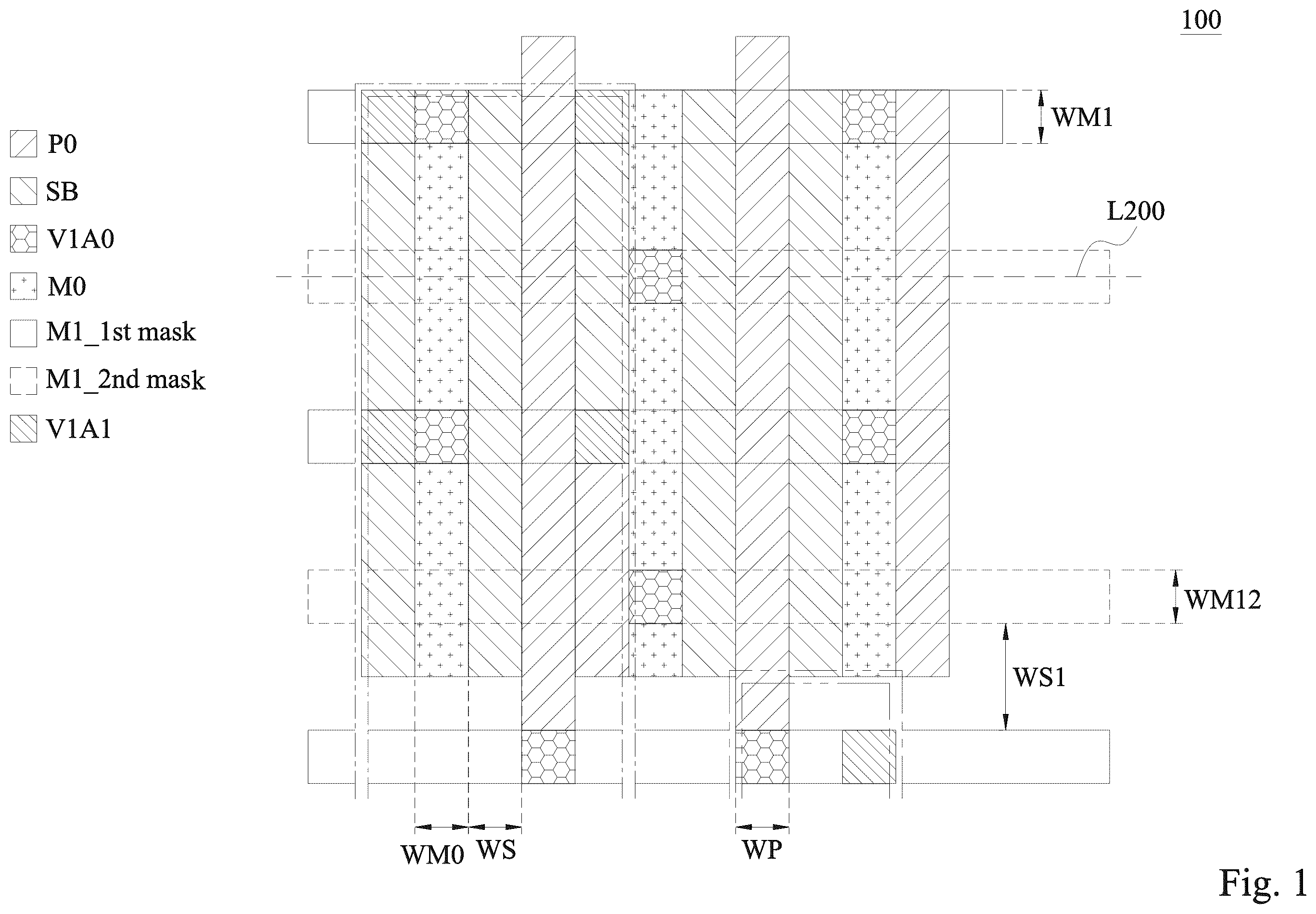
is a layout diagram of a semiconductor structure 100 , in accordance with some embodiments. is a cross section diagram 200 at line L 200 of semiconductor structure 100 , in accordance with some embodiments. Labels for different sub-structures of semiconductor structure 100 are illustratively provided in .
Semiconductor structure 100 is used to form different electrical devices, including transistors, for example. As illustratively shown in , structure 100 includes a substrate SB, two poly structures PO, a metal layer M 0 having three metal strips, eight vias VIA 0 , five vias VIA 1 , a metal line in metal layer M 1 formed by a first mask, and a metal line in metal layer M 1 formed by a second mask. A metal strip is also called a metal structure. Various other semiconductor structures different from semiconductor structure 100 are within the contemplated scope of the present disclosure.
A region or a portion of a poly structure PO is used to form a gate of a transistor. An oxide diffusion (OD) region or a portion of substrate SB is used to form a drain or a source of a transistor. Vias VIA 0 are used to connect electrical components in metal layer M 0 to metal layer M 1 . Vias VIA 1 are used to connect electrical components in metal layer M 1 to metal layer M 2 . In various embodiments of the present disclosure, a source of a transistor functions as a drain and vice versa. Semiconductor 100 is of a fin field effect transistor (FinFET) type, but planar or other technologies are within the contemplated scope of the present disclosure.
A width WM 0 indicates a width of a metal strip M 0 in metal M 0 layer. A width WM 11 indicates a width of a metal strip in a metal M 1 layer formed by a first mask, such as mask M 10 in B . A width WM 12 indicates a width of a metal strip in a metal M 1 layer formed by a second mask, such as mask M 20 in F . A width WS 1 indicates a distance between two metal strips in a metal M 1 layer. A width WS indicates a distance between a metal strip M 0 to a poly structure PO. A width WP indicates a width of a poly structure PO. In some embodiments, a width WP is proportional to a channel length of a transistor. For example, a transistor having a larger channel length has a larger width WP, and vice versa. Two similar currents of two transistors having two larger widths WP have a lower mismatch than the same two similar currents of the same two transistors having two smaller widths WP. In some embodiments, to reduce current mismatch in similar circuits with similar transistors, poly structures PO having larger widths WP are used. Transistors in a circuit that are formed by the same or different widths WP are within the contemplated scope of the disclosure. In some embodiments, width WP is equal to or greater than each of width WM 0 , WM 11 , or WM 12 . In some embodiments, widths WM 0 , WM 11 , and WM 12 are of a same size, but widths WM 0 , WM 11 , and WM 12 are of different sizes in other embodiments.
For illustration, each of widths WM 0 , WS, WP, WS 1 , WM 11 , WM 12 is called a distance unit, and is used to determine whether a conductive line is long or not. For example, in some embodiments, a conductive line is considered long if the conductive line is at least five distance units. In some embodiments, the smallest width among the widths is used as the distance unit. Five distance units are used as an example. Another number of distance units are within the contemplated scope of the disclosures. Various ways to determine whether a conductive line is long is within the contemplated scope of the disclosure.
is a diagram of a circuit 300 , in accordance with some embodiments. Circuit 300 is an inverter ring that includes three inverters connected in series. The first inverter is formed by a PMOS transistor MP 1 and an NMOS transistor MN 1 . The second inverter is formed by a PMOS transistor MP 2 and an NMOS transistor MN 2 , and the third inverter is formed by a PMOS transistor MP 3 and an NMOS transistor MN 3 . An output of the first inverter is coupled with an input of the second inverter. An output of the second inverter is coupled with an input of the third inverter, and an output of the third inverter is coupled with an input of the first inverter.
In various embodiments, a conductive line LDD_P 1 _N 1 between the drain of transistor MP 1 and the drain of transistor MN 1 is considered long, and is formed by a second mask, such as a mask M 20 in F . Similarly, a conductive line LDD_P 2 _N 2 between the drain of transistor MP 2 and the drain of transistor MN 2 and a conductive line LDD_P 3 _N 3 between the drain of transistor MP 3 and the drain of transistor MN 3 are each considered long, and are each formed by mask M 20 .
Additionally, conductive lines LDG_N 1 _N 2 , LDG_N 2 _N 3 , LGD_P 1 _P 3 are considered long and are formed by mask M 20 . Conductive line LDG_N 1 _N 2 connects the drain of transistor N 1 and the gate of transistor N 2 . Because the drain of transistor MP 1 is coupled to the drain of transistor MN 1 , and the gate of transistor MP 2 is coupled to the gate of transistor MN 2 , the drains of transistors MP 1 , MN 1 , MP 2 , and MN 2 are coupled together by conductive line LDG_N 1 _N 2 . Similarly, through conductive line LDG_N 2 _N 3 , the drains of transistor MP 2 , MN 2 and the gates of transistors MP 3 , MN 3 are coupled together. Conductive line LGD_P 1 _P 3 connects the gate of transistor P 1 and the drain of transistor P 3 . Because the gate of transistor MP 1 is coupled to the gate of transistor MN 1 , and the drain of transistor MP 3 is coupled to the drain of transistor MN 3 , the gates of transistors MP 1 , MN 1 , and the drains of transistor MP 3 , MN 3 are coupled together by conductive line LGD_P 1 _P 3 . In various embodiments, conductive lines, including conductive lines LDD_P 1 _N 1 , LDG_N 1 _N 2 , LDD_P 3 _N 3 , etc., are surrounded by dielectric material, such as dielectric material of dielectric lay 170 in C .
is a layout diagram of a semiconductor structure 400 , in accordance with some embodiments. Semiconductor structure 400 includes six semiconductor structures 100 - 1 to 100 - 6 that form circuit 300 in . Semiconductor structures 100 - 1 , 100 - 2 , 100 - 3 , 100 - 4 , 100 - 5 , and 100 - 6 form transistors MP 1 , MN 1 , MP 2 , MN 2 , MP 3 , and MN 3 in , respectively. Poly structures PO_P 1 , PO_P 2 , PO_P 3 , PO_N 1 , PO_N 2 , and PO_N 3 are used to form the gates of transistor MP 1 , MP 2 , MP 3 , MN 1 , MN 2 , and MN 3 , respectively. Substrates SB of structures 100 - 1 , 100 - 2 , 100 - 3 , 100 - 4 , 100 - 5 , and 100 - 6 are called SB- 1 , SB- 2 , SB- 3 , SB- 4 , SB- 5 , and SB- 6 , respectively, but, for simplicity, are not labeled in . Each of substrates SB- 1 , SB- 2 , SB- 3 , SB- 4 , SB- 5 , and SB- 6 includes OD regions to form the drains and the sources of respective transistors MP 1 , MP 2 , MP 3 , MN 1 , MN 2 , and MN 3 . For simplicity, various elements of transistors MP 1 , MP 2 , MP 3 , MN 1 , MN 2 , and MN 3 in and are not labeled.
Lines L 510 , L 520 , and L 530 are discussed with reference to .
is a cross-section diagram 500 at line L 510 of , in accordance with some embodiments. Cross section diagram 500 is used to illustrate a connection between the drain of transistor MP 1 and the drain of transistor MN 1 by conductive line LDD_P 1 _N 1 .
OD regions S_P 1 and D_P 1 are parts of substrate SB- 1 in . OD region S_P 1 forms a source of transistor MP 1 . OD region D_P 1 forms a drain of transistor MP 1 . Poly region G_P 1 on poly structure PO_P 1 in forms a gate of transistor MP 1 .
OD regions S_N 1 and D_N 1 are part of substrate SB- 2 in . OD region S_N 1 forms a source of transistor MN 1 . OD region D_N 1 forms a drain of transistor MN 1 . Poly region G_N 1 on poly structure PO_N 1 in forms a gate of transistor MP 1 .
As illustratively shown in , drain region D_P 1 is electrically coupled with metal piece M 0 - 1 , via VIA 0 - 10 , conductive line LDD_P 1 _N 1 , via VIA 0 - 20 , metal piece M 0 - 2 and drain region D_N 1 . Effectively, conductive line LDD_P 1 _N 1 electrically connects the drain of transistor MP 1 and the drain of transistor MN 1 .
In some embodiments as illustrated in , conductive line LDD_P 1 _N 1 is considered long because conductive line LDD_P 1 _N 1 extends beyond one semiconductor structure. For example, conductive line LDD_P 1 _N 1 extends across semiconductor structure 100 - 1 and semiconductor structure 100 - 2 . Considered in another way, conductive line LDD_P 1 _N 1 is long because conductive line LDD_P 1 _N 1 is longer than a predetermined length. For example, conductive line LDD_P 1 _N 1 from via VIA 0 - 10 to via VIA 0 - 20 is longer than five distance units because the conductive line from via VIA 0 - 10 to via VIA- 20 expands at least the distance units of via VIA 0 - 10 , poly region G_P 1 , metal piece M 0 - 11 , metal piece M 0 - 21 , and poly region G_N 1 . Considered in yet another way, conductive line LDD_P 1 _N 1 is long because conductive line LDD_P 1 _N 1 carries a current from the drain of transistor MP 1 to the drain of transistor MN 1 , which is relatively large compared with another current in another part of circuit 300 , such as a current between the gate of transistor MP 1 and the gate of transistor MN 1 . In some embodiments, because conductive line LDD_P 1 _N 1 is considered long, conductive line LDD_P 1 _N 1 is formed by a second and succeeding mask M 20 in F in a in a self-aligned double patterning (SADP) technology. Other ways to form conductive line LDD_P 1 _N 1 such that a resistivity and/or an RC constant on conductive line LDD_P 1 _N 1 decrease are within the contemplated scope of the present disclosure.
Because of similarities of semiconductor structures 100 - 1 and 100 - 2 to corresponding semiconductor structure 100 - 3 and 100 - 4 , a connection between the drain of transistor P 2 and the drain of transistor N 2 through conductive line LDD_P 2 _N 2 is similar to the connection between the drain of transistor P 1 and the drain of transistor N 1 through conductive line LDD_P 1 _N 1 . For example, with reference to conductive line LDD_P 2 _N 2 , a cross section diagram at line L 520 in is similar to cross section diagram 500 in . Similarly, a connection between the drain of transistor P 3 and the drain of transistor N 3 through conductive line LDD_P 3 _N 3 is similar to the connection between the drain of transistor P 1 and the drain of transistor N 1 through conductive line LDD_P 1 _N 1 . For example, with reference to conductive line LDD_P 3 _N 3 , a cross section diagram at line L 530 in is similar to cross section diagram 500 in .
A is a layout diagram of semiconductor structure 400 in reproduced to have labels associated with B and 6 C . A- 6 C are used to illustrate a connection between the drain of transistor MN 1 and the gate of transistor MN 2 by conductive line LDG_N 1 _N 2 shown in .
B is a cross-section diagram 600 B at line L 610 of A , in accordance with some embodiments. Metal piece M 1 - 620 in B is not visible in A . As illustratively shown in B , conductive line LDG_N 1 _N 2 is connected with vias VIA 1 - 10 and VIA 1 - 20 . Via VIA 1 - 20 is coupled with metal piece M 1 - 620 , via VIO 0 - 420 , and poly PO_N 2 that is the gate of transistor MN 2 . C is a cross-section diagram 600 C at line L 620 of A . Diagram 600 C is used to illustrate a connection between via VIA 1 - 10 and the drain of transistor MN 1 . As illustratively shown, via VIA 1 - 10 is coupled with conductive line LDD_P 1 _N 1 , via VIA 0 - 20 , metal piece M 0 - 2 , and OD region D_N 1 that is the drain of transistor MN 1 . Effectively, conductive line LDG_N 1 _N 2 connects the drain of transistor MN 1 to the gate of transistor MN 2 .
A connection between the drain of transistor MP 1 and the drain of transistor MN 1 is illustrated above with reference to . A connection between the gate of transistor MP 2 and the gate of transistor MN 2 is similar to the connection between the gate of transistor MP 1 and the gate of transistor MN 1 as illustrated with reference to C . Effectively, conductive line LDG_N 1 _N 2 connects the drains of transistors MP 1 , MN 1 and the gates of transistors MP 2 , MN 2 .
A connection between the drains of transistors MP 2 , MN 2 and the gates of transistors MP 3 , MN 3 through conductive line LDG_N 2 _N 3 is similar to the connection between the drains of transistors MP 1 , MN 1 and the gates of transistor MP 2 , MN 2 through conductive line LDG_N 1 _N 2 .
In some embodiments, conductive lines LDG_N 1 _N 2 , LDG_N 2 _N 3 are considered long based on various factors as described with reference to conductive line LDD_P 1 _N 1 . As a result, in some embodiments, conductive lines LDG_N 1 _N 2 , LDG_N 2 _N 3 are formed by mask M 20 .
A is a layout diagram of semiconductor structure 400 reproduced having labels related B, 7 C, and 7 D . A- 7 D are used to illustrate a connection between a gate of transistor MP 1 and a drain of transistor MP 3 by conductive line LGD_P 1 _P 3 shown in .
B is a cross-section diagram 700 B at line L 710 of A , in accordance with some embodiments. As illustratively shown in B , conductive line LGD_P 1 _P 3 is connected with vias VIA 1 - 30 and VIA 1 - 40 . Further, via VIA 1 - 30 is coupled with line LGG_P 1 _N 1 , via VIA 0 - 30 , and poly structure PO_P 1 that forms the gate of transistor MP 1 .
C is a cross-section diagram 700 C at line L 740 in A , in accordance with some embodiments. In C , conductive line LGD_P 1 _P 3 is coupled with via VIA 1 - 40 , metal piece M 1 _ 71 , via VIA 0 _ 71 , metal piece M 0 _ 71 , and region D_P 3 that forms the drain of transistor P 3 . Effectively, conductive line LGD_P 1 _P 3 connects the gate of transistor MP 1 and the drain of transistor MP 3 .
D is a cross-section diagram 700 D at line L 720 in A , in accordance with some embodiments.
In D , poly structure PO_P 1 is coupled with via VIA 0 - 30 , line LGG_P 1 _N 1 , via VIA 0 - 40 , and poly structure PO_N 1 . Because poly structure PO_P 1 forms the gate of transistor MP 1 and poly structure PO_N 1 forms the gate of transistor MN 1 , effectively, the gate of transistor MP 1 is coupled with the gate of transistor MN 1 . A connection between the drain of transistor MP 3 and the drain of transistor MN 3 is similar to the connection between the drain of transistor MP 1 and the drain of transistor MN 1 as illustratively shown in . Effectively, conductive line LGD_P 1 _P 3 connects the gates of transistors MP 1 , MN 1 and the drains of transistors MP 3 , MN 3 .
In some embodiments, conductive line LGD_P 1 _P 3 is considered long based on various factors as described with reference to conductive line LDD_P 1 _N 1 . As a result, in some embodiments, conductive line LGD_P 1 _P 3 is formed by mask M 20 .
Similar Circuits
Various embodiments of the present disclosure include similar circuits. For example, in some embodiments regarding a symmetrical circuit having a first circuit similar to second circuit, conductive lines are configured such that performance of the first circuit is substantially the same as performance of the second circuit. For another example, in some embodiments, conductive lines in the first circuit and in the second circuit are configured to meet at least one of the following conditions: a resistivity of a conductive line in the first circuit is substantially the same as a resistivity of a corresponding conductive line in the second circuit, an RC constant of a conductive line in the first circuit is substantially the same as an RC constant of a corresponding conductive line in the second circuit, and/or a first current in the first circuit is substantially the same as a second current in the corresponding second circuit. A current mirror that has a current in a first branch substantially the same as a current in a second branch is an exemplary circuit that can benefit from various embodiments of the present disclosure. Various pairs of similar circuits and/or symmetrical circuits are within the contemplated scope of the present disclosure.
is a diagram of an exemplary symmetrical circuit 800 , in accordance with some embodiments. Circuit 800 includes a circuit 810 L symmetrical with a circuit 810 R with reference to a line 810 . As illustratively shown, circuit 810 L includes nine PMOS transistors MP 6 <A,B,C>, MP 5 <A,B,C>, and MP 4 <A,B,C> corresponding to nine PMOS transistors MP 3 <A,B,C>, MP 2 <A,B,C>, and MP 1 <A,B,C>, respectively, in circuit 810 R.
In various embodiments, conductive lines to connect various terminals of transistors MP 1 <A,B,C> to MP 6 <A,B,C> in circuits 810 L and 810 R are configured such that a current I 1 in circuit 810 L is substantially the same as a current I 2 in circuit 810 R. Current I 1 flows from sources of transistors MP 6 <A,B,C> through transistors MP 6 <A,B,C>, MP 5 <A,B,C>, and MP 4 <A,B,C> to drains of transistors MP 4 <A,B,C>. Current I 2 flows from sources of transistors MP 3 <A,B,C> through transistors MP 3 <A,B,C>, MP 2 <A,B,C>, and MP 1 <A,B,C> to drains of transistors MP 1 <A,B,C>.
In various embodiments, when a conductive line in circuit 810 L is formed by a mask, such as mask M 10 in F , for example, a corresponding conductive line in circuit 810 R is formed by the same mask M 10 . Similarly, when a conductive line in circuit 810 L is formed by another mask, such as mask M 20 in F , a corresponding conductive line in circuit 810 R is formed by the same mask M 20 . As illustratively shown in , conductive line L 850 L connects the drains of transistors MP 6 <A,B,C> and the sources of transistor MP 5 <A,B,C>, and corresponds to conductive line L 850 R that connects the drains of transistors MP 3 <A,B,C> and the sources of transistor MP 2 <A,B,C>. Similarly, conductive line L 860 L connects the drains of transistors MP 5 <A,B,C> and the sources of transistor MP 4 <A,B,C> and corresponds to conductive line L 860 R that connects the drains of transistors MP 2 <A,B,C> and the sources of transistor MP 1 <A,B,C>. Other conductive lines in circuit 810 L corresponding to conductive lines in circuit 810 R are within the contemplated scope of the present disclosure.
is a detailed circuit diagram of circuit 810 R in , in accordance with some embodiments. As illustratively shown, gates of transistors MP 3 <A>, MP 3 <B>, MP 3 <C> are coupled together. Sources of transistors MP 3 <A>, MP 3 <B>, MP 3 <C> are coupled together by a conductive line LSSS_ 3 A_ 3 B_ 3 C. Drains of transistors MP 3 <A>, MP 3 <B>, MP 3 <C> are coupled together by a conductive line LDDD_ 3 A_ 3 B_ 3 C, and are also coupled with sources of transistors MP 2 <A>, MP 2 <B>, MP 2 <C>.
Gates of transistors MP 2 <A>, MP 2 <B>, MP 2 <C> are coupled together. Drains of transistors MP 2 <A>, MP 2 <B>, MP 2 <C> are coupled together by a conductive line LDD_ 2 A_ 2 B_ 2 C, and are also coupled with sources of transistors MP 1 <A>, MP 1 <B>, MP 1 <C>.
Gates of transistors MP 1 <A>, MP 1 <B>, MP 1 <C> are coupled together. Drains of transistors MP 1 <A>, MP 1 <B>, MP 1 <C> are coupled by a conductive line LDDD_ 1 A_ 1 B_ 1 C.
In some embodiments, conductive lines LSSS_ 3 A_ 3 B_ 3 C, LDDD_ 3 A_ 3 B_ 3 C, LDDD_ 2 A_ 2 B 2 C, and LDDD_ 1 A_ 1 B_ 1 C are each considered long based on various factors as described with reference to conductive line LDD_P 1 _N 1 , and are formed by mask M 20 in F . Additionally, conductive lines in circuit 810 L corresponding to conductive lines LSSS_ 3 A_ 3 B_ 3 C, LDDD_ 3 A_ 3 B_ 3 C, LDDD_ 2 A_ 2 B_ 2 C, and LDDD_ 1 A_ 1 B_ 1 C are also considered long and are formed by mask M 20 .
In some embodiments, the drain of transistor MP 3 <A> and the source of transistor MP 2 <A> are formed by the same OD region. Effectively, the drain of transistor MP 3 <A> is coupled with the source of transistor MP 2 <A>. Similarly, the drain of transistor MP 2 <A> and the source of transistor MP 1 <A> are formed by the same OD region. Effectively, the drain of transistor MP 2 <A> is coupled with the source of transistor MP 1 <A>. A connection between a drain of transistor MP 3 <B> and a source of transistor MP 2 <B> and a connection between a drain of transistor MP 3 <C> and a source of transistor MP 2 <C> are each similar to the connection between the drain of transistor MP 3 <A> and the source of transistor MP 2 <A>. Similarly, a connection between a drain of transistor MP 2 <B> and a source of transistor MP 1 <B> and a connection between a drain of transistor MP 2 <C> and a source of transistor MP 1 <C> is similar to a connection between the drain of transistor MP 2 <A> and the source of transistor MP 1 <A>.
is a layout diagram of a semiconductor structure 1000 , in accordance with some embodiments. Semiconductor structure 1000 is used to form circuit 810 R in . Circuit 810 L in is formed by a semiconductor structure similar to semiconductor structure 1000 . Structure 1000 includes a first sub-structure PA, a second sub-structure PB, and a third sub-structure PC. Sub-structure PA is used to form transistors MP 3 <A>, MP 2 <A>, MP 1 <A>. Sub-structure PB is used to form transistors MP 3 <B>, MP 2 <B>, MP 1 <B>, and substructure PC is used to form transistors MP 3 <C>, MP 2 <C>, MP 1 <C>. For simplicity, various elements associated with sub-structure PB and sub-structure PC are not labeled, but are similar to those associated with sub-structure PA. Sub-structures PA, PB, and PC each have various structure elements similar to those of structure 100 in , including, for example, poly structures PO, substrate SB, vias VIA 0 , etc.
For illustration, sub-structures PA, PB, and PC include corresponding substrates SB-A, SB-B, and SB-C shown in .
Poly structures PO_ 3 A, PO_ 2 A, PO_ 1 A are used to form the gates of transistors MP 3 <A>, MP 2 <A>, MP 1 <A>, respectively.
Lines L 1100 , L 1210 , L 1220 , and L 1230 are lines for cross-section diagrams explained with reference to respectively.
is a cross section diagram 1100 at line L 1100 in , in accordance with some embodiments. Diagram 1100 is used to illustrate a connection between a drain of transistor MP 3 <A> and a source of transistor MP 2 <A>, and between a drain of transistor MP 2 <A> and a source of transistor MP 1 <A>. In some embodiments, as illustratively shown in , the drain of transistor MP 3 <A> is formed by OD region D 3 A, which is also used to form the source of transistor MP 2 <A>. For illustration, OD region D 3 A is also called OD region S 2 A. Similarly, the drain of transistor MP 2 <A> is formed by OD region D 2 A, which is also used to form the source of transistor MP 1 <A>, and is also called OD region S 1 A.
A connection between a drain of transistor MP 3 <B> and a source of transistor MP 2 <B>, and between a drain of transistor MP 2 <B> and a source of transistor MP 1 <B> is similar to the connection between a drain of transistor MP 3 <A> and a source of transistor MP 2 <A>, and between a drain of transistor MP 2 <A> and a source of transistor MP 1 <A>, respectively. Further, a connection between a drain of transistor MP 3 <C> and a source of transistor MP 2 <C>, and between a drain of transistor MP 2 <C> and a source of transistor MP 1 <C> is similar to the connection between a drain of transistor MP 3 <A> and a source of transistor MP 2 <A>, and between a drain of transistor MP 2 <A> and a source of transistor MP 1 <A>, respectively.
is a cross section diagram 1200 at line L 1210 in , in accordance with some embodiments. Diagram 1200 is used to illustrate a connection between drains of transistors MP 3 <A>, MP 3 <B>, and MP 3 <C>. In , the drains of transistors MP 3 <A>, MP 3 <B>, MP 3 <C> are formed by OD regions D 3 A, D 3 B, and D 3 C, respectively. As illustratively shown in , OD regions D 3 A, D 3 B, D 3 C are coupled with metal pieces M 0 - 122 , M 0 - 124 , M 0 - 126 , respectively, and with vias VIA 0 - 122 , VIA 0 - 124 , VIA 0 - 126 , respectively. Further, conductive line LDDD_ 3 A_ 3 B_ 3 C is coupled with vias VIA 0 - 122 , VIA 0 - 124 , and VIA 0 - 126 . Effectively, conductive line LDDD_ 3 A_ 3 B_ 3 C couples the drains of transistors MP 3 <A>, MP 3 <B>, MP 3 <C> together.
In a same manner as conductive line LDDD_ 3 A_ 3 B_ 3 C connects the drains of transistors MP 3 <A>, MP 3 <B>, MP 3 <C>, conductive line LDDD_ 2 A_ 2 B_ 2 C connects the drains of transistors MP 2 <A>, MP 2 <B>, MP 2 <C>, conductive line LDDD_ 1 A_ 1 B_ 1 C connects the drains of transistors MP 1 <A>, MP 1 <B>, MP 1 <C>, and conductive line LSSS_ 3 A_ 3 B_ 3 C connects the sources of transistors MP 3 <A>, MP 3 <B>, MP 3 <C>. For example, a cross section diagram at each line L 1220 , L 1230 , and L 1240 in is similar to cross section diagram 1200 in .
In various embodiments, conductive lines LSSS_A_ 3 B_ 3 C LDDD_ 3 A_ 3 B_ 3 C, LDDD_ 2 A_ 2 B_ 2 C, LDDD_ 1 A_ 1 B_ 1 C are each considered long based on various factors as described with reference to conductive line LDD_P 1 _N 1 , and are each formed by mask M 20 in F .
A is a diagram of circuit 810 R in reproduced with label related to B and 12 C . A-C are used to illustrate another way to connect the drain of transistor MP 3 <A> to the source of transistor MP 2 <A> and the source of transistor MP 2 <B>, in accordance with some embodiments.
B is a layout diagram of a semiconductor structure 1200 B, in accordance with some embodiments. Semiconductor structure 1200 B is used to form a portion of circuit 810 R in A . For example, structure 1200 B is used to form transistors MP 3 <A,B>, MP 2 <A,B> and MP 1 <A,B>, and without transistors MP 3 <C>, MP 2 <C>, MP 1 <C> in A .
Structure 1200 B includes a first sub-structure P 01 , a second sub-structure P 02 , and a third sub-structure P 03 . Sub-structure P 01 is used to form transistors MP 1 <A>, MP 1 <B>. Sub-structure P 02 is used to form transistors MP 2 <A>, MP 2 <B>, and substructure P 03 is used to form transistors MP 3 <A>, MP 3 <B>. For simplicity, various elements associated with sub-structures P 01 , P 02 , P 03 are not labeled. Sub-structures P 01 , P 02 , and P 03 each have various structure elements similar to those of structure 100 in , including, for example, poly structures PO, substrate SB, vias VIA 0 , etc.
For illustration, sub-structures P 01 , P 02 , and P 03 include substrates SB- 01 , SB- 02 , and SB- 03 , respectively, which are labeled in C . Sub-structure P 01 includes poly structure PO_ 1 A, PO_ 1 B. Sub-structure P 02 includes poly structure PO_ 2 A, PO_ 2 B, and sub-structure P 03 includes poly structure PO_ 3 A, PO_ 3 B. Poly structures PO_ 3 A, PO_ 2 A, PO_ 1 A are used to form the gates of transistors MP 3 <A>, MP 2 <A>, MP 1 <A>, respectively. Poly structures PO_ 3 B, PO_ 2 B, PO_ 1 B are used to form the gates of transistors MP 3 <B>, MP 2 <B>, MP 1 <B>, respectively. Corresponding OD regions in sub-structures P 01 , P 02 , and P 03 are used to form the drains and the sources of transistors MP 1 <A,B>, MP 2 <A,B>, and MP 3 <A,B> respectively.
Lines L 1260 and L 1270 are used for cross-section diagrams explained with reference to C .
C is a cross section diagram 1200 C at line L 1260 in A , in accordance with some embodiments. Diagram 1200 C is used to illustrate a connection between the drain of transistor MP 3 <A>, the source of transistor MP 2 <A>, and the source of transistor MP 2 <B> by conductive line LDSS_ 3 A_ 2 A_ 2 B.
OD regions DO 3 A, SO 2 A, and SO 2 B form the drain, the source, and the source of transistors MP 3 <A>, MP 2 <A>, and MP 2 <B>, respectively.
In some embodiments, as illustratively shown in C , OD region DO 3 A is coupled with metal piece M 0 - 32 , via VIA 0 - 55 , and conductive line LDSS_ 3 A_ 2 A_ 2 B. OD region SO 2 A is coupled with metal piece M 0 - 34 , via VIA 0 - 65 , and conductive line LDSS_ 3 A_ 2 A_ 2 B. OD region SO 2 B is coupled with metal piece M 0 - 36 , via VIA 0 - 75 , and conductive line LDSS_ 3 A_ 2 A_ 2 B. Effectively, conductive line LDSS_ 3 A_ 2 A_ 2 B connects the drain, the source, and the source of corresponding transistors MP 3 <A>, MP 2 <A>, and MP 2 <B>.
Conductive line LDSS_ 2 A_ 1 A_ 1 B connects the drain, the source, and the source of corresponding transistors MP 2 <A>, MP 1 <A>, and MP 1 <B> in a same manner as conductive line LDSS_ 3 A_ 2 A_ 2 B connects the drain, the source, and the source of corresponding transistors MP 3 <A>, MP 2 <A>, and MP 2 <B>. For example, a cross section diagram at line L 1270 is similar to cross section diagram 1200 C in C , but, for simplicity, is not shown.
Sub-structure P 01 forming two transistors MP 1 <A>, MP 1 <B> is for illustration. Sub-structure P 01 forming additional transistors is within the contemplated scope of the present disclosure. For example, additional poly structures are added to form gates of the additional transistors. Corresponding OD regions in substrate SB- 01 form sources and drains of the additional transistors. For another example, a poly structure PO_ 1 C (not labeled) is added to sub-structure P 01 to form the gate of transistor MP 1 <C>. Corresponding OD regions DO 1 C (not labeled) and SO 1 C (not labeled) in substrate SB- 01 are used to form the drain and the source of transistor MP 1 <C>. Forming additional transistors in sub-structures P 03 and P 02 is done in a manner similar to forming additional transistors in substructure P 01 . When additional transistors are formed in corresponding sub-structures P 01 , P 02 , and P 03 , conductive lines LDSS_ 3 A_ 2 A_ 2 B and LDSS_ 2 A_ 1 A_ 1 B are extended to connect terminals of corresponding additional transistors. For example, when transistors MP 3 <C>, MP 2 <C>, and MP< 1 C> are added to corresponding sub-structures P 03 , P 02 , and P 01 , conductive line LDSS_ 3 A_ 2 A_ 2 B is extended to connect the source of transistor MP 2 <C>. In such a situation, effectively, conductive line LDSS_ 3 A_ 2 A_ 2 B connects the drain, the source, the source, and the source of corresponding transistors MP 3 <A>, MP 2 <A>, MP 2 <B>, and MP 2 <C>. Similarly, conductive line LDSS_ 2 A_ 1 A_ 1 B is extended to connect the source of transistor MP 1 <C>. In such a situation, conductive line LDSS_ 2 A_ 1 A_ 1 B connects the drain, the source, the source, and the source of corresponding transistors MP 2 <A>, MP 1 <A>, MP 1 <B>, MP 1 <C>, etc.
In various embodiments, conductive line LDSS_ 3 A_ 2 A_ 2 B and conductive line LDSS_ 2 A_ 1 A_ 1 B are each considered long based on various factors as discussed with reference to conductive line LDD_P 1 _N 1 , and are each formed by mask 20 M in F .
As illustrated in and A- 12 C , different semiconductor structures are used to form the same circuit 810 R, resulting in different conductive lines connecting the same terminals of various transistors. For example, conductive line
LDD_ 3 A_ 3 B_ 3 C in connects the drains of transistors MP 3 <A,B,C>. Conductive line LDSS_ 3 A_ 2 A_ 2 B in A effectively connects the drains of the same transistors MP 3 <A,B,C>. In various embodiments of the present disclosure, regardless of the semiconductor structures being used to form transistors and/or other devices, when a conductive line is considered long, a current, a resistivity and/or a RC constant of a conductive line is decided to be reduced, the conductive line is formed to have a wider width by using second mask M 20 , for example.
Forming Conductive Lines
A- 13 K are diagrams used to illustrate how conductive lines are formed by a first mask or a second mask, in accordance with some embodiments. For illustration, the first mask is called mask M 10 , and is shown in B . The second mask is called mask M 20 , and is shown in F . Further, long conductive lines are formed by mask M 20 , and other conductive lines are formed by mask M 10 . Additionally, conductive lines A- 5 and A- 15 in K are formed by first mask M 10 and have a width smaller than that of conductive line B- 10 formed by second mask M 20 . Conductive line A- 5 thus corresponds to conductive line LGG_P 1 _N 1 in C while conductive line B- 10 corresponds to long conductive lines LDD_P 1 _N 1 , LDD_P 2 _N 2 , LDD_P 3 _N 3 , etc.
With reference to A , a pattern 130 - 5 represents conductive line A- 5 in K , and a pattern 130 - 15 represents conductive line A- 15 . Expressed in another way, pattern 130 - 5 is used to form conductive line A- 5 , and pattern 130 - 15 is used to form conductive line A- 15 . Similarly, pattern 130 - 10 is used to form conductive line B- 10 . In some embodiments, patterns 130 - 5 , 130 - 10 , and 130 - 15 are included in a graphic database system (GDS) file. In some embodiments, conductive lines A- 5 and A- 15 have a same width XA. For simplicity, forming conductive line A- 5 is described, but the same procedure to form conductive line A- 5 is also applicable to form conductive line A- 15 . Conductive line B- 10 has a width XB. Because patterns 130 - 5 and 130 - 15 are used to form conductive lines A- 5 and A- 15 , in some embodiments, patterns 130 - 5 and 130 - 15 are each associated with width XA stored in a data file, for example. Similarly, pattern 130 - 10 is associated with width XB. In some embodiments, widths XA and XB are provided in the data file when a layout for circuits that use conductive lines A- 5 and B- 5 are designed, such as, when the layout is drawn in a computer. As a result, a size of width XA and/or XB may be adjusted during the layout design stage. In some embodiments, patterns 130 - 5 and 130 - 15 are associated with a color of mask M 10 and pattern 130 - 10 is associated with a color of mask M 20 . Alternatively expressed, forming conductive lines A- 5 and B- 10 is based on corresponding colors of patterns 130 - 5 and 130 - 10 .
B is a diagram of mask M 10 , in accordance with some embodiments. Mask M 10 has patterns 140 - 5 , 140 - 10 , and 140 - 115 corresponding to patterns 130 - 5 , 130 - 10 , and 130 - 15 in A , respectively.
In some embodiments, pattern 140 - 5 has a width XA 2 S, which is the total of width XA plus two widths XS of spacers 190 - 3 and 190 - 7 in E . Alternatively expressed, width XA 2 S is designed to accommodate spacers 190 - 3 and 190 - 7 . In some embodiments, a size of each of spacers 190 - 3 and 190 - 7 is used to determine a size of opening 150 - 5 in C . Width XA 2 S is therefore determined accordingly. In some embodiments, width XS is the same for various spacers associated with mask M 10 , including, for example, spacers 190 - 8 , 190 - 12 , etc., in E . In some embodiments, width WS of spacers 190 - 3 , 190 - 5 , 190 - 7 , 190 - 8 , 190 - 12 is designed such that a distance DAB between conductive line A- 5 and conductive line B- 10 in K is equal to or greater than a predetermined value, which is called a minimum space value between conductive line A- 15 and conductive line B- 10 .
Pattern 140 - 10 has width XB of conductive line B- 10 , which is the same as a width of pattern 150 - 10 in C .
C is a cross section diagram of a structure 1300 C, in accordance with some embodiments. In C , a hard mask layer 150 is above a buffer layer 160 , which, in turn, is above a dielectric layer 170 . Openings 150 - 5 and 150 - 15 of hard mask layer 150 are a result of an etch operation on layer 150 based on patterns 140 - 5 and 140 - 15 in B . Pattern 150 - 10 includes the hard mask material of hard mask layer 150 after forming openings 150 - 5 and 150 - 15 .
In some embodiments, buffer layer 160 is added in between hard mask layer 150 and dielectric layer 170 to protect dielectric layer 170 . For example, buffer layer 160 prevents potential damage to layer 170 due to the stress of layer 180 in D onto dielectric layer 170 . In some embodiments, dielectric layer 170 surrounds metal strips in corresponding metal layers.
D is a cross-section diagram of a structure 1300 D, in accordance with some embodiments. Structure 1300 D is a result of structure 1300 C being deposited with a layer 180 of spacer material. Layer 180 includes openings 180 - 5 and 180 - 15 corresponding to patterns 130 - 5 and 130 - 15 in A , respectively. Each of openings 180 - 5 and 180 - 15 has width XA corresponding to width XA of conductive lines A- 5 and A- 15 in K . A height Y 180 of layer 180 is selected such that after an etch process to form structure 1300 E in E , a thickness of layer 190 in E is substantially the same as a thickness of hard mask layer 150 . Effectively, height Y 180 is a function of a thickness of mask layer 150 .
In some embodiments, the exposed surface of layer 180 including the bottom of opening 180 - 5 is etched at the same time. In some embodiments, etching includes bombarding ion to the surface of layer 180 and the bottom of opening 180 - 5 . When the bottom of opening 180 - 5 reaches the surface of layer 160 , the surface of layer 180 is leveled with the surface of pattern 150 - 10 , the etch operation stops, resulting in structure 1300 E in E . As illustratively shown in E , a portion of spacer material in layer 180 in structure 1300 D has been removed to result in four spacers 190 - 3 , 190 - 7 , 190 - 8 , and 190 - 12 . Effectively, based on a thickness of hard mask layer 150 , layer 190 is formed to have spacers 190 - 3 , 190 - 7 , 190 - 8 , 190 - 12 , pattern 150 - 10 , and other hard mask material that, for simplicity, is not labeled.
Spacers 190 - 3 and 190 - 7 define opening 190 - 5 . Spacers 190 - 7 and 190 - 8 are adjacent to hard mask pattern 150 - 10 . In some embodiments, a surface of layer 190 is substantially flat. For example, the surface of pattern 150 - 10 and of spacers 190 - 3 , 190 - 7 , 190 - 8 , and 190 - 12 are of about a same level. Openings 180 - 5 and 180 - 15 in D result in corresponding openings 190 - 5 and 190 - 15 having bottoms at a surface of layer 160 .
F is used to illustrate second mask M 20 is used to etch structure 1300 E to result in structure 1300 G in G . For simplicity, elements of structures 1300 E are not labeled in F . In F , mask M 20 has pattern 220 - 10 corresponding to pattern 150 - 10 , and patterns 200 - 5 , 200 - 15 corresponding to openings 190 - 5 , 190 - 15 , respectively. Patterns 200 - 5 and 200 - 15 are to prevent opening 190 - 5 and 190 - 15 from being etched.
Pattern 200 - 10 is to etch and thus remove hard mask pattern 150 - 10 . In some embodiments, a width of pattern 200 - 10 is equal to or greater than a width of hard mask pattern 150 - 10 , which, in some embodiments, is XB. In case the width of mask pattern 200 - 10 is greater than the width of hard mask pattern 150 - 10 , the etch operation does not etch through spacers 190 - 3 , 190 - 7 , 190 - 8 , or 190 - 12 , because, in some embodiments, spacer material in layer 180 that forms spacers 190 - 3 , 190 - 7 , 190 - 8 , and 190 - 12 is selected to stand against etching operation. In other words, during etching away pattern 150 - 10 , opening 210 - 10 in G is conformed to width XB of pattern 150 - 10 that is defined by spacers 190 - 7 and 190 - 8 .
H is a cross-section diagram of a structure 1300 H, in accordance with some embodiments. Structure 1300 H is a result of structure 1300 G being etched into dielectric layer 170 and resulting in openings 220 - 5 , 220 - 10 , 220 - 15 . Effectively, based on openings 190 - 5 , 210 - 10 , and 190 - 15 , an etch operation etches through buffer layer 160 into dielectric layer 170 .
I is a diagram of a structure 1300 I, in accordance with some embodiments. Structure 1300 I is the result of structure 1300 H having layers 190 and 160 removed. Structure 1300 I has openings 230 - 5 , 230 - 10 , and 230 - 15 , which are called trenches of dielectric layer 170 .
J is a diagram of a structure 1300 J, in accordance with some embodiments. Structure 1300 J is the result of structure 1300 I having been filled with a layer 250 of conductive material, which, in some embodiments, is metal. The conductive material fills over trenches 230 - 5 , 230 - 10 , 230 - 15 and surface 235 of dielectric layer 170 .
K is a diagram of a structure 1300 K, in accordance with some embodiments. Structure 1300 K is the result of structure 1300 J being processed with a chemical mechanical process (CMP) operation. In some embodiments, the CMP operation removes conductive material on top of surface 235 and leaves behind conductive material in trenches 230 - 5 , 230 - 10 , 230 - 15 to form conductive lines A- 5 , B- 10 , and A- 15 , respectively. Effectively, conductive lines A- 5 , B- 10 , and A- 15 are surrounded by dielectric material of dielectric layer 170 . A number of embodiments have been described. It will nevertheless be understood that various modifications may be made without departing from the spirit and scope of the disclosure. For example, in various embodiments, when signal traces draw a larger amount of currents, conductive lines with a wider width are formed for those signal traces. For another example, in some embodiments, a current flowing through a drain and/or a source is much higher than a current flowing through a gate of the same transistor. In those embodiments, conductive lines related to the drain and/or the source are formed having a wider width, by, for example, using second mask M 20 .
is a flowchart a method 1400 of forming conductive lines used in a circuit, in accordance with some embodiments.
In operation 1410 , the signal traces are grouped into a first group of first signal traces and a second group of second signal traces. In some embodiments, the first signal traces have a first width, and the second signal traces have a second width different from the first width. Further, the grouping is based on at least one of the following conditions: a current flowing through a signal trace of the signal traces, a length of the signal trace, a resistivity of the signal trace, or a resistive-capacitive constant of the signal trace.
In operation 1420 , a first mask, such as mask M 10 , is used to form first conductive lines for the first signal traces of the first group and a second mask, such as mask M 20 , is used to form second conductive lines for the second signal traces of the second group.
is a flowchart 1500 illustrating a method of forming conductive lines, in accordance with some embodiments.
In some embodiments, operations of flowchart 1500 are based on a first mask used to form a first conductive line and a second mask used to form a second conductive line. In operation 1510 , the first mask, such as mask M 10 , and a second mask, such as mask M 20 , are identified.
In operation 1520 , the first mask is used to form a third conductive line if a width of the first conductive line is larger than a width of the second conductive line or the second mask is used to form the third conductive line if the width of the second conductive line is larger than the width of the first conductive line. In some embodiments, the third conductive line connects a first circuit element distant from a second circuit element by a predetermined value.
is a flowchart 1600 illustrating another method of forming conductive lines, in accordance with some embodiments.
In some embodiments, the flowchart 1600 is based on a first circuit similar to a second circuit, a first mask used to form first conductive lines having a first width, a second mask used to form second conductive lines having a second width different from the first width. In some embodiments, the first mask is mask M 10 and the second mask is mask M 20 .
In operation 1610 , the first mask is used to form third conductive lines of the first circuit and fourth conductive lines of the second circuit. In some embodiments, each conductive line of the third conductive lines corresponds to each conductive line of the fourth conductive lines.
In operation 1620 , the second mask is used to form fifth conductive lines of the first circuit and sixth conductive lines of the second circuit. In some embodiments, each conductive line of the fifth conductive lines corresponds to each conductive line of the sixth conductive lines. Further, the third conductive lines of the first circuit carry respective first currents and fifth conductive lines of the first circuit carry respective second currents, and a current value of the first currents is less than a current value of the second currents.
The above illustrations are based on two masks, masks M 10 and M 20 . However, more than two masks may be used. For example, the inventive concepts disclosed herein are applicable in multi-patterning technology including self-aligned multi-patterning. Similarly to the two mask situations, each mask of the more than two mask situations is used to form a set of conductive lines. In various embodiments, a succeeding mask used to form a set of conductive lines having a width larger than a width of conductive lines formed by a preceding mask. For example, if three masks are used in the order of masks MA 10 , MA 20 , and MA 30 , conductive lines formed by second mask MA 20 have a width larger than that of conductive lines formed by first mask MA 10 , and conductive lines formed by third mask MA 30 have a width larger than that of conductive lines formed by second mask MA 20 .
However, other widths of conductive lines corresponding to other orders of masks being used to form the conductive lines are within the contemplated scope of the present disclosure. Explained in a different way, conductive lines having a larger width are formed regardless of the order of the masks being used to form the conductive lines. For example, mask MA 10 may be used to form conductive lines having a width larger than one or both widths of conductive lines formed by mask MA 20 or mask MA 30 . For another example, in the above illustrations, first mask M 10 provides conductive line A- 5 having a width smaller than a width of conductive line B- 10 formed by second mask M 20 . In other embodiments, first mask M 10 provides conductive lines having a width larger than a width of conductive lines formed by second mask M 20 . In such situations, conductive lines formed by first mask M 10 are used for long signal trances.
Other ways to form different sets of conductive lines each set having a different width are within the contemplated scope of the present disclosure. Various circuits, including inverter ring 300 , are used for illustration purposes. Other circuits are within the contemplated scope of the present disclosure.
In some embodiments, a method is disclosed. The method includes identifying at least a first mask or a second mask, fabricating, by the first mask, a first conductive line, fabricating, by the second mask, a second conductive line; and fabricating, by the first mask, a third conductive line if a dimension of the first conductive line is larger than a corresponding dimension of the second conductive line; or fabricating, by the second mask, the third conductive line if the dimension of the first conductive line is less than the corresponding dimension of the second conductive line. In some embodiments, a first circuit element is coupled to a second circuit element by at least the third conductive line, and the first circuit element is separated from the second circuit element by a predetermined distance.
In some embodiments, a method is disclosed. The method includes identifying at least a first mask or a second mask; fabricating, by a first mask, a first conductive line having a first width; fabricating, by a second mask, a second conductive line having a second width less than the first width; and fabricating, by the first mask, a third conductive line having the first width. In some embodiments, the third conductive line couples a first circuit element to a second circuit element, and the first circuit element is separated from the second circuit element by a predetermined distance.
In some embodiments, a method is disclosed. The method includes fabricating, by a first mask, a first set of conductive lines having a first dimension; fabricating, by a second mask, a second set of conductive lines having a second dimension, the first dimension being different from the second dimension; and fabricating, by the first mask, a third set of conductive lines of a first circuit and a fourth set of conductive lines of a second circuit. In some embodiments, the first circuit is similar to the second circuit, each conductive line of the third set of conductive lines corresponds to each conductive line of the fourth set of conductive lines, and each conductive line of the third set of conductive lines is configured to carry a corresponding first current.
Various transistors being shown as a particular dopant type (e.g., N-type or P-type Metal Oxide Semiconductor (NMOS or PMOS)) are for illustration purposes. Embodiments of the disclosure are not limited to a particular type. Selecting different dopant types for a particular transistor is within the scope of various embodiments. The low or high logical value of various signals used in the above description is also for illustration. Various embodiments are not limited to a particular logical value when a signal is activated and/or deactivated. Selecting different logical values is within the scope of various embodiments. In various embodiments, a transistor functions as a switch. In various embodiments, a source of a transistor can be configured as a drain, and a drain can be configured as a source. In some embodiments, a first value is substantially the same as a second value when a ratio between the first value over the second value is greater than about 90%. Other ratio values and/or different ways to determine whether the first value is substantially the same as the second value are within the contemplated scope of the present disclosure. Exemplary ratio values include 87%, 85%, 80%, etc.
The above illustrations include exemplary steps, but the steps are not necessarily performed in the order shown. Steps may be added, replaced, changed order, and/or eliminated as appropriate, in accordance with the spirit and scope of disclosed embodiments.
Figures (20)
Citations
This patent cites (24)
- US6038383
- US7999393
- US8601416
- US8762900
- US8775993
- US8887116
- US10360314
- US2002/0022311
- US2004/0031010
- US2008/0169862
- US2008/0303776
- US2010/0207248
- US2011/0053096
- US2013/0049211
- US2014/0101623
- US2014/0201692
- US2014/0237435
- US2014/0282337
- US2014/0304670
- US2014/0310675
- US2014/0325464
- US10-0542533
- US10-2009-0084758
- US10-1016826