Abstract
An integrated circuit device includes: a fin-type active region on a substrate and including a fin top surface at a first level; a gate line on the fin-type active region; and an insulating structure on a sidewall of the fin-type active region. The insulating structure includes: a first insulating liner in contact with a sidewall of the fin-type active region; a second insulating liner on the first insulating liner and including an uppermost portion at a second level c than the first level; a lower buried insulating layer facing the sidewall of the fin-type active region and including a first top surface facing the gate line at a third level lower than the second level; and an upper buried insulating layer between the lower buried insulating layer and the gate line and including a second top surface at a fourth level equal to or higher than the second level.
Claims (20)
1. An integrated circuit device, comprising: a fin-type active region extending in a first horizontal direction on a substrate and comprising a fin top surface; a nanosheet stack comprising at least one nanosheet on the fin top surface, the nanosheet stack being spaced apart from the fin top surface in a vertical direction; a gate line extending in a second horizontal direction crossing the first horizontal direction on the fin-type active region, the gate line surrounding the at least one nanosheet; and an insulating structure between the substrate and the gate line and on a sidewall of the fin-type active region, wherein the insulating structure comprises: a lower buried insulating layer comprising a first top surface facing the gate line, the first top surface being closer to a bottom surface of the substrate than the fin top surface; an upper buried insulating layer between the lower buried insulating layer and the gate line, the upper buried insulating layer comprising a second top surface facing the gate line, the second top surface being farther from the bottom surface of the substrate than the first top surface; and an upper insulating liner between the sidewall of the fin-type active region and the upper buried insulating layer and between the lower buried insulating layer and the upper buried insulating layer.
11. An integrated circuit device, comprising: a substrate comprising a device region and an inter-device isolation region defining the device region; a fin-type active region extending in a first horizontal direction in the device region and comprising a fin top surface; a nanosheet stack comprising at least one nanosheet on the fin top surface, the nanosheet stack being spaced apart from the fin top surface in a vertical direction; a gate line extending in a second horizontal direction crossing the first horizontal direction in the device region and the inter-device isolation region, the gate line surrounding the at least one nanosheet on the fin-type active region; a first insulating structure between the substrate and the gate line in the device region and on a sidewall of the fin-type active region; and a second insulating structure between the substrate and the gate line in the inter-device isolation region, wherein the first insulating structure comprises: a first lower buried insulating layer on the sidewall of the fin-type active region, the first lower buried insulating layer comprising a first top surface facing the gate line, the first top surface being closer to a bottom surface of the substrate than the fin top surface; a first upper buried insulating layer between the first lower buried insulating layer and the gate line, the first upper buried insulating layer comprising a second top surface facing the gate line, the second top surface being farther from the bottom surface of the substrate than the first top surface; and a first upper insulating liner between the sidewall of the fin-type active region and the first upper buried insulating layer and between the first lower buried insulating layer and the first upper buried insulating layer.
17. An integrated circuit device, comprising: a substrate comprising a first region and a second region spaced apart from each other; a first fin-type active region defined by a first device isolation trench in the first region, the first fin-type active region comprising a first fin top surface at a first level; at least one nanosheet on the first fin top surface; a first gate line on the first fin-type active region, the first gate line surrounding the at least one nanosheet on the first fin top surface; a second fin-type active region defined by a second device isolation trench in the second region, the second fin-type active region comprising a second fin top surface higher, relative to a bottom surface of the substrate, than the first fin top surface; a second gate line on the second fin-type active region, the second gate line surrounding the second fin top surface and sidewalls of the second fin-type active region; a first insulating structure on a sidewall of the first fin-type active region in the first region; and a second insulating structure on a sidewall of the second fin-type active region in the second region, wherein each of the first insulating structure and the second insulating structure comprises: a lower buried insulating layer comprising a first top surface closer to a bottom surface of the substrate than the first level; an upper buried insulating layer comprising a second top surface farther from the bottom surface of the substrate than the first top surface; and an upper insulating liner between the lower buried insulating layer and the upper buried insulating layer.
Show 17 dependent claims
2. The integrated circuit device of claim 1 , wherein the upper buried insulating layer is spaced apart from the fin-type active region with the upper insulating liner between the upper buried insulating layer and the fin-type active region.
3. The integrated circuit device of claim 1 , wherein the upper insulating liner comprises a first part overlying the lower buried insulating layer in the vertical direction, and a second part that is closer to the sidewall of the fin-type active region than both of the lower buried insulating layer and the upper buried insulating layer.
4. The integrated circuit device of claim 1 , wherein the upper buried insulating layer comprises a silicon oxide layer comprising at least one impurity element comprising at least one of nitrogen (N) and fluorine (F).
5. The integrated circuit device of claim 1 , wherein the upper buried insulating layer comprises: a first silicon oxide layer comprising at least one of nitrogen (N) atom and fluorine (F); and a second silicon oxide layer between the first silicon oxide layer and the gate line.
6. The integrated circuit device of claim 1 , wherein the first top surface of the lower buried insulating layer has a concave shape toward the gate line, and wherein a bottom surface of the upper buried insulating layer faces the first top surface of the lower buried insulating layer and has a convex shape toward the substrate.
7. The integrated circuit device of claim 1 , wherein at least a portion of the second top surface of the upper buried insulating layer has a planar shape extending in the second horizontal direction.
8. The integrated circuit device of claim 1 , wherein at least a portion of the second top surface of the upper buried insulating layer has a convex shape toward the gate line.
9. The integrated circuit device of claim 1 , wherein at least a portion of the second top surface of the upper buried insulating layer has a concave shape toward the gate line.
10. The integrated circuit device of claim 1 , wherein each of the lower buried insulating layer and the upper insulating liner comprises a silicon oxide layer, wherein the upper buried insulating layer comprises a silicon oxide layer comprising at least one of nitrogen (N) and fluorine (F), and wherein a density of the lower buried insulating layer is lower than a respective density of each of the upper insulating liner and the upper buried insulating layer.
12. The integrated circuit device of claim 11 , wherein the second insulating structure comprises: a second lower buried insulating layer between the substrate and the gate line, the second lower buried insulating layer comprising a third top surface facing the gate line, the third top surface being farther from the bottom surface of the substrate than the first top surface of the first lower buried insulating layer; and a second upper buried insulating layer between the second lower buried insulating layer and the gate line, the second upper buried insulating layer comprising a fourth top surface facing the gate line, the fourth top surface being farther from the bottom surface of the substrate than the second top surface of the first upper buried insulating layer.
13. The integrated circuit device of claim 11 , wherein the second insulating structure comprises: a second lower buried insulating layer between the substrate and the gate line; and a second upper buried insulating layer between the second lower buried insulating layer and the gate line, and wherein each of the first upper buried insulating layer and the second upper buried insulating layer comprises a silicon oxide layer comprising at least one of nitrogen (N) and fluorine (F).
14. The integrated circuit device of claim 11 , wherein the second insulating structure comprises: a second lower buried insulating layer between the substrate and the gate line; and a second upper buried insulating layer between the second lower buried insulating layer and the gate line, and wherein each of the first upper buried insulating layer and the second upper buried insulating layer comprises: a first silicon oxide layer comprising at least one of nitrogen (N) and fluorine (F); and a second silicon oxide layer between the first silicon oxide layer and the gate line.
15. The integrated circuit device of claim 11 , wherein the second insulating structure comprises: a second lower buried insulating layer between the substrate and the gate line, the second lower buried insulating layer comprising a third top surface facing the gate line, the third top surface being farther from the bottom surface of the substrate than the first top surface of the first lower buried insulating layer; a second upper buried insulating layer between the second lower buried insulating layer and the gate line, the second upper buried insulating layer comprising a fourth top surface facing the gate line, the fourth top surface being farther from the bottom surface of the substrate than the second top surface of the first upper buried insulating layer; and a second upper insulating liner between the second lower buried insulating layer and the second upper buried insulating layer, wherein the first upper buried insulating layer is spaced apart from the fin-type active region with the first upper insulating liner between the first upper buried insulating layer and the fin-type active region, and wherein the second upper buried insulating layer is spaced apart from the fin-type active region with the second upper insulating liner between the second upper buried insulating layer and the fin-type active region.
16. The integrated circuit device of claim 11 , wherein the second insulating structure comprises: a second lower buried insulating layer between the substrate and the gate line; and a second upper buried insulating layer between the second lower buried insulating layer and the gate line, wherein the first lower buried insulating layer comprises a first silicon oxide layer having a first density, and wherein the second lower buried insulating layer comprises a second silicon oxide layer having a second density greater than the first density.
18. The integrated circuit device of claim 17 , wherein the upper buried insulating layer is spaced apart from the first fin-type active region with the upper insulating liner between the upper buried insulating layer and the first fin-type active region in the first region.
19. The integrated circuit device of claim 17 , wherein the upper insulating liner comprises a first part overlying the lower buried insulating layer in the vertical direction, and a second part that is closer to the sidewall of the first fin-type active region than both of the lower buried insulating layer and the upper buried insulating layer.
20. The integrated circuit device of claim 17 , wherein the upper buried insulating layer comprises a silicon oxide layer comprising at least one of nitrogen (N) and fluorine (F) in each of the first region and the second region.
Full Description
Show full text →
CROSS-REFERENCE TO RELATED APPLICATION
This application is a continuation of and claims priority to U.S. patent application Ser. No. 17/379,051, filed Jul. 19, 2021, which is based on and claims priority under 35 U.S.C. § 119 to Korean Patent Application No. 10-2020-0183522, filed on Dec. 24, 2020, in the Korean Intellectual Property Office, the disclosures of which are incorporated by reference herein in their entirety.
BACKGROUND
The inventive concepts relate to integrated circuit devices, and more particularly, to integrated circuit devices including a field-effect transistor.
Recently, as down-scaling of integrated circuit devices is rapidly progressing, it is beneficial for an integrated circuit device to secure not only a fast operation speed but also accuracy of operation. In addition, as the degree of integration of integrated circuit device increases and the size of integrated circuit devices is reduced, there is a need for the development of a new structure capable of improving the performance and reliability of a nanosheet field-effect transistor.
SUMMARY
The inventive concepts provide integrated circuit devices having a structure capable of improving the performance of a transistor and reducing power consumption by reducing parasitic capacitance between adjacent conductive regions.
According to an aspect of the inventive concepts, there is provided an integrated circuit device including a fin-type active region extending in a first horizontal direction on a substrate and including a fin top surface at a first level; a gate line extending in a second horizontal direction crossing the first horizontal direction on the fin-type active region; and an insulating structure between the substrate and the gate line and on a sidewall of the fin-type active region, wherein the insulating structure includes a first insulating liner in contact with a sidewall of the fin-type active region; a second insulating liner on the sidewall of the fin-type active region with the first insulating liner therebetween and including an uppermost portion at a second level that is closer to a bottom surface of the substrate than the first level; a lower buried insulating layer on the sidewall of the fin-type active region with the first insulating liner and the second insulating liner therebetween and including a first top surface facing the gate line at a third level that is closer to the bottom surface of the substrate than the second level; and, an upper buried insulating layer between the lower buried insulating layer and the gate line and including a second top surface at a fourth level that is at a same distance or farther from the bottom surface of the substrate than the second level.
According to another aspect of the inventive concepts, there is provided an integrated circuit device including a substrate including a device region and an inter-device isolation region defining the device region; a fin-type active region extending in a first horizontal direction in the device region and including a fin top surface at a first level; a nanosheet stack including at least one nanosheet on the fin top surface and spaced apart from the fin top surface in a vertical direction, each nanosheet of the nanosheet stack having a different vertical distance from the fin top surface; a gate line on the at least one nanosheet on the fin-type active region, the gate line extending in a second horizontal direction crossing the first horizontal direction in the device region and the inter-device isolation region; a first insulating structure between the substrate and the gate line in the device region and on a sidewall of the fin-type active region; and a second insulating structure between the substrate and the gate line in the inter-device isolation region, wherein the first insulating structure includes a first insulating liner in contact with the sidewall of the fin-type active region; a second insulating liner on the sidewall of the fin-type active region with the first insulating liner therebetween and including an uppermost portion at a second level that is closer to a bottom surface of the substrate than the first level; a first lower buried insulating layer on the sidewall of the fin-type active region with the first insulating liner and the second insulating liner therebetween, and comprising a first top surface facing the gate line at a third level that is closer to the bottom surface of the substrate than the second level; and a first upper buried insulating layer between the first lower buried insulating layer and the gate line and comprising a second top surface at a fourth level that is at a same distance or farther from the bottom surface of the substrate than the second level.
According to another aspect of the inventive concepts, there is provided an integrated circuit device including a substrate including a first region and a second region spaced apart from each other, the substrate further including a first device isolation trench disposed in the first region and a second device isolation trench disposed in the second region, a first fin-type active region defined by the first device isolation trench in the first region, at least one nanosheet on a first fin top surface of the first fin-type active region and spaced apart from the first fin top surface in a vertical direction, a second fin-type active region defined by the second device isolation trench in the second region and including a second fin top surface higher, relative to a bottom surface of the substrate, than the first fin top surface; a first insulating structure on a sidewall of the first fin-type active region in the first region, and a second insulating structure on a sidewall of the second fin-type active region in the second region, wherein each of the first insulating structure and the second insulating structure device regions a first insulating liner in contact with the substrate; a second insulating liner on the first insulating liner and including an uppermost portion at a second level that is lower, relative to the bottom surface of the substrate, than a first level of the first fin top surface; a lower buried insulating layer on the second insulating liner and including a first top surface at a third level that is lower, relative to the bottom surface of the substrate, than the second level; and an upper buried insulating layer on the uppermost portion of the second insulating liner and the first top surface of the lower buried insulating layer and including a second top surface at a fourth level that is equal to or higher, relative to the bottom surface of the substrate, than the second level.
BRIEF DESCRIPTION OF THE DRAWINGS
Embodiments of the inventive concepts will be more clearly understood from the following detailed description taken in conjunction with the accompanying drawings in which:
is a plan layout diagram of some components of an integrated circuit device according to an embodiment of the inventive concepts;
A is a cross-sectional view showing a partial configuration of a cross-section taken along line X 1 -X 1 ′ of , B is a cross-sectional view showing a partial configuration of a cross-section taken along line X 2 -X 2 ′ of , C is a cross-sectional view showing a partial configuration of a cross-section taken along line Y 1 -Y 1 ′ of , and D is an enlarged cross-sectional view of some components included in a region indicated as “EQ” in C ;
is a cross-sectional view illustrating an integrated circuit device according to an embodiment of the inventive concepts;
is a cross-sectional view illustrating an integrated circuit device according to an embodiment of the inventive concepts;
is a cross-sectional view illustrating an integrated circuit device according to an embodiment of the inventive concepts;
is a cross-sectional view illustrating an integrated circuit device according to an embodiment of the inventive concepts;
is a cross-sectional view illustrating an integrated circuit device according to an embodiment of the inventive concepts;
is a block diagram of an integrated circuit device according to an embodiment of the inventive concept;
is a plan layout diagram illustrating a partial configuration of a second region of the integrated circuit device illustrated in ;
is a cross-sectional view showing a partial configuration of a cross-section taken along line Y 4 -Y 4 ′ of ; and
A to 20 D are cross-sectional views illustrating methods of manufacturing an integrated circuit device according to embodiments of the inventive concepts, wherein A, 12 A , . . . , and 20 A are cross-sectional views showing a partial configuration of a portion corresponding to a cross-section taken along line X 1 -X 1 ′ of , B, 12 B , . . . , and 20 B are cross-sectional views showing a partial configuration of a portion corresponding to a cross-section taken along line X 2 -X 2 ′ of , C, 12 C , . . . , and 20 C are cross-sectional views showing a partial configuration of a portion corresponding to a cross-section taken along line Y 1 -Y 1 ′ of , and D, 12 D , . . . , and 20 D are cross-sectional views showing a partial configuration of a portion corresponding to a cross-section taken along line Y 4 -Y 4 ′ of .
DETAILED DESCRIPTION
Hereinafter, embodiments of the inventive concepts will be described in detail with reference to the accompanying drawings. The same reference numerals are used for the same elements in the drawings, and redundant descriptions thereof are omitted.
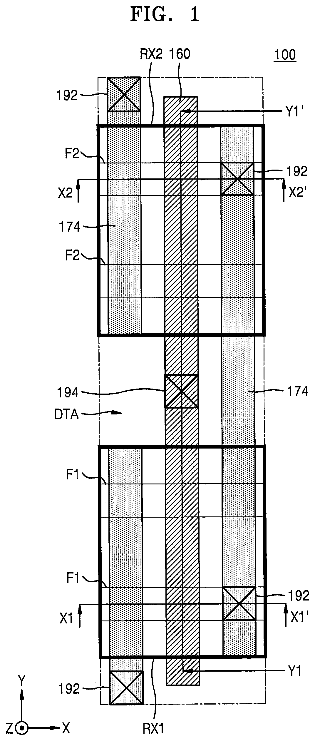
is a plan layout diagram of some components of an integrated circuit device according to an embodiment of the inventive concepts. A is a cross-sectional view showing a partial configuration of a cross-section taken along line X 1 -X 1 ′ of , B is a cross-sectional view showing a partial configuration of a cross-section taken along line X 2 -X 2 ′ of , C is a cross-sectional view showing a partial configuration of a cross-section taken along line Y 1 -Y 1 ′ of , and D is an enlarged cross-sectional view of some components included in a region indicated as “EQ” in C .
Referring to A to 2 D , the integrated circuit device 100 may include a first device region RX 1 and a second device region RX 2 , and a substrate 102 including an inter-device isolation area DTA therebetween. A deep trench DTR may be formed in the substrate 102 in the inter-device isolation area DTA. The first device region RX 1 and the second device region RX 2 may be defined by the deep trench DTR.
The substrate 102 may include a semiconductor such as Si or Ge, or a compound semiconductor such as SiGe, SiC, GaAs, InAs, InGaAs, or InP. The terms “SiGe”, “SiC”, “GaAs”, “InAs”, “InGaAs”, and “InP” as used herein mean materials including elements included in the respective terms, and are not equations representing stoichiometric relationships. The substrate 102 may include a conductive region, for example, a well doped with an impurity, or a structure doped with an impurity.
In the first device region RX 1 and the second device region RX 2 , a plurality of fin-type active regions F 1 and F 2 may protrude from the substrate 102 in a vertical direction (e.g., a Z direction). The plurality of fin-type active regions F 1 and F 2 may extend parallel to each other in a first horizontal direction (e.g., an X direction). The plurality of fin-type active regions F 1 and F 2 may be defined by device isolation trenches STR formed in the substrate 102 in the first device region RX 1 and the second device region RX 2 , respectively.
The plurality of fin-type active regions F 1 and F 2 may include the plurality of first fin-type active regions F 1 arranged in the first device region RX 1 and the plurality of second fin-type active regions F 2 arranged in the second device region RX 2 . Each of the plurality of fin-type active regions F 1 and F 2 may have a fin top surface FT of a first level LV 1 . The term “level” as used herein means a height in a vertical direction (e.g., the Z direction or −Z direction) from a bottom surface of the substrate 102 . illustrates two first fin-type active regions F 1 disposed in the first device region RX 1 and two second fin-type active regions F 2 disposed in the second device region RX 2 , but one or three or more fin-type active regions F 1 and F 2 may be disposed in the first device region RX 1 and the second device region RX 2 , respectively.
On the plurality of fin-type active regions F 1 and F 2 , a gate line 160 extends long in a second horizontal direction (e.g., a Y direction) crossing the first horizontal direction (X direction). illustrates a configuration in which one gate line 160 is disposed on the plurality of fin-type active regions F 1 and F 2 , but the number of gate lines 160 on the plurality of fin-type active regions F 1 and F 2 is not limited thereto. For example, a plurality of gate lines 160 may be disposed on each of the plurality of fin-type active regions F 1 and F 2 .
A first insulating structure ST 1 may be filled in the device isolation trench STR in the first device region RX 1 and the second device region RX 2 . The first insulating structure ST 1 may be disposed between the substrate 102 and the gate line 160 and may cover a sidewall of each of the plurality of fin-type active regions F 1 and F 2 .
The first insulating structure ST 1 may include a first insulating liner 112 A, a second insulating liner 112 B, a first lower buried insulating layer 112 C, a first upper insulating liner 114 S, and a first upper buried insulating layer 116 S that are sequentially stacked on the substrate 102 .
The first insulating liner 112 A may contact sidewalls of each of the plurality of fin-type active regions F 1 and F 2 . An uppermost portion of the first insulating liner 112 A may be equal to or lower (e.g., closer to the substrate 102 ) than the first level LV 1 of the fin top surface FT. The second insulating liner 112 B may be on and/or face the sidewall of each of the plurality of fin-type active regions F 1 and F 2 with the first insulating liner 112 A therebetween. As used herein, the term “and/or” includes any and all combinations of one or more of the associated listed items. The second insulating liner 112 B may have an uppermost portion of a second level LV 2 lower (e.g., closer to the substrate 102 ) than the first level LV 1 .
The first lower buried insulating layer 112 C may be on and/or face the sidewall of each of the plurality of fin-type active regions F 1 and F 2 with the first insulating liner 112 A and the second insulating liner 112 B therebetween. A top surface of the first lower buried insulating layer 112 C facing the gate line 160 may non-linearly extend in the second horizontal direction (e.g., the Y direction) at a level lower than the second level LV 2 . A top surface of the first lower buried insulating layer 112 C facing the gate line 160 may have a concave shape toward the gate line 160 . A lowermost portion of the top surface of the first lower buried insulating layer 112 C may be a third level LV 3 lower than the second level LV 2 .
A first height H 1 that is a distance in the vertical direction (e.g., the Z direction) from the fin top surface FT of each of the plurality of fin-type active regions F 1 and F 2 to the second level LV 2 that is a level of the uppermost portion of the second insulating liner 112 B may be greater than zero. A second height H 2 that is a distance in the vertical direction (e.g., the Z direction) from the fin top surface FT of each of the plurality of fin-type active regions F 1 and F 2 to the third level LV 3 that is a level of a lowermost portion of the top surface of the first lower buried insulating layer 112 C may be greater than the first height H 1 .
The first upper insulating liner 114 S may be interposed between the second insulating liner 112 B and the first upper buried insulating layer 116 S, and between the first lower buried insulating layer 112 C and the first upper buried insulating layer 116 S. The first upper insulating liner 114 S may include a portion in contact with an uppermost portion of the second insulating liner 112 B and a portion in contact with a top surface of the first lower buried insulating layer 112 C.
The first upper buried insulating layer 116 S may be interposed between the first lower buried insulating layer 112 C and the gate line 160 . The first upper insulating liner 114 S may be interposed between a top surface of the first lower buried insulating layer 112 C and a bottom surface of the first upper buried insulating layer 116 S.
A top surface of the first upper buried insulating layer 116 S may extend flatly in the horizontal direction (e.g., the X direction and the Y direction) at a fourth level LV 4 higher (e.g., farther from the substrate 102 ) than the second level LV 2 . The bottom surface of the first upper buried insulating layer 116 S may face the top surface of the first lower buried insulating layer 112 C with the first upper insulating liner 114 S therebetween, and have a convex shape toward the substrate 102 corresponding to a concave shape of the top surface of the first lower buried insulating layer 112 C.
A third height H 3 that is a distance in the vertical direction (e.g., the Z direction) from the fin top surface FT of each of the plurality of fin-type active regions F 1 and F 2 to the fourth level LV 4 that is a level of the top surface of the first upper buried insulating layer 116 S may be greater than or equal to zero. In some embodiments, the third height H 3 may be equal to or smaller than the first height H 1 . That is, the level of the top surface of the first upper buried insulating layer 116 S may be equal to or higher than the level of the uppermost portion of the second insulating liner 112 B.
In some embodiments, the first insulating liner 112 A and the second insulating liner 112 B may include different materials. For example, the first insulating liner 112 A may include a silicon oxide layer, and the second insulating liner 112 B may include a silicon nitride layer.
In some embodiments, each of the first lower buried insulating layer 112 C and the first upper insulating liner 114 S may include a silicon oxide layer. The first upper buried insulating layer 116 S may include a silicon oxide layer including at least one impurity element selected from a nitrogen (N) atom and/or a fluorine (F) atom. Expressions such as “at least one of,” when preceding a list of elements, modify the entire list of elements and do not modify the individual elements of the list. In some embodiments, a density of the silicon oxide layer constituting the first lower buried insulating layer 112 C may be lower than a density of each of the first upper insulating liner 114 S and the first upper buried insulating layer 116 S.
A second insulating structure ST 2 may be disposed between the substrate 102 and the gate line 160 in the inter-device isolation area DTA. The second insulating structure ST 2 may fill in a deep trench DTR. The second insulating structure ST 2 may be spaced apart from the plurality of fin-type active regions F 1 and F 2 in the second horizontal direction (e.g., the Y direction).
The second insulating structure ST 2 may include a second lower buried insulating layer 113 , a second upper insulating liner 114 D, and a second upper buried insulating layer 116 D that are sequentially stacked on the substrate 102 .
At least a part of a top surface of the second lower buried insulating layer 113 may be at a level higher than the top surface of the first lower buried insulating layer 112 C. The top surface of the first lower buried insulating layer 112 C may have an uppermost portion of a fifth level LV 5 higher than the third level LV 3 .
The second upper buried insulating layer 116 D may be interposed between the second lower buried insulating layer 113 and the gate line 160 . The second upper insulating liner 114 D may be interposed between the top surface of the second lower buried insulating layer 113 and the bottom surface of the second upper buried insulating layer 116 D.
The second upper buried insulating layer 116 D may have a top surface that extends flatly in the horizontal direction (e.g., the X and the Y directions) at a sixth level LV 6 higher than the fourth level LV 4 that is a level of a top surface of the first upper buried insulating layer 116 S.
The top surface of the second lower buried insulating layer 113 may have a convex shape toward the gate line 160 . A bottom surface of the second upper buried insulating layer 116 D may face the top surface of the second lower buried insulating layer 113 with the second upper insulating liner 114 D therebetween, and have a concave shape toward the substrate 102 corresponding to a convex shape of the top surface of the second lower buried insulating layer 113 .
Each of the second lower buried insulating layer 113 and the second upper insulating liner 114 D may include a silicon oxide layer. In some embodiments, a density of the silicon oxide layer constituting each of the second lower buried insulating layer 113 and the second upper insulating liner 114 D may be higher than a density of the silicon oxide layer constituting the first lower buried insulating layer 112 C. The second upper buried insulating layer 116 D may include a silicon oxide layer including at least one impurity element selected from a nitrogen (N) atom and a fluorine (F) atom. In some embodiments, the first upper insulating liner 114 S and the second upper insulating liner 114 D may include the same material, and the first upper buried insulating layer 116 S and the second upper buried insulating layer 116 D may include the same material. In some embodiments, a content of the impurity element in each of the first upper buried insulating layer 116 S and the second upper buried insulating layer 116 D may be about 0.1 atomic % to about 20 atomic %, but is not limited thereto.
The gate line 160 may extend in the second horizontal direction (e.g., the Y direction) on the plurality of fin-type active regions F 1 and F 2 , the first insulating structure ST 1 , and the second insulating structure ST 2 . A plurality of nanosheet stacks NSS may be disposed on the fin top surface FT of each of the plurality of fin-type active regions F 1 and F 2 in regions where the plurality of fin-type active regions F 1 and F 2 and the gate line 160 cross each other. The plurality of nanosheet stacks NSS may face the fin top surface FT at positions spaced apart from the plurality of fin-type active regions F 1 and F 2 in the vertical direction (e.g., the Z direction), respectively.
The plurality of nanosheet stacks NSS may include a plurality of nanosheets N 1 , N 2 , and N 3 overlapping each other in the vertical direction (e.g., the Z direction) on the fin top surface FT of each of the fin-type active regions F 1 and F 2 . The term “nanosheet” as used herein refers to a conductive structure having a cross-section substantially perpendicular to a direction in which a current flows in the conductive structure. It should be understood that the nanosheets may include nanowires. The plurality of nanosheets N 1 , N 2 , and N 3 may have different vertical distances (e.g., Z-direction distances) from the fin top surface FT. The plurality of nanosheets N 1 , N 2 , and N 3 may include the first nanosheet N 1 , the second nanosheet N 2 , and the third nanosheet N 3 that are sequentially stacked on the fin top surface FT of the fin-type active regions F 1 and F 2 .
The number of the nanosheet stacks NSS and the gate lines 160 disposed on one fin-type active region F 1 or F 2 is not limited to those in the figures. For example, one or a plurality of nanosheet stacks NSS and one or a plurality of gate lines 160 may be disposed on one fin-type active region F 1 or F 2 .
A to 2 D illustrate a case in which each of the plurality of nanosheet stacks NSS includes the three nanosheets N 1 , N 2 , and N 3 , but the embodiments of the inventive concepts are not limited thereto. The number of nanosheets constituting the nanosheet stack NSS is not particularly limited. For example, each of the plurality of nanosheet stacks NSS may include one, two, or four or more nanosheets. Each of the plurality of nanosheets N 1 , N 2 , and N 3 may have a channel region. For example, each of the plurality of nanosheets N 1 , N 2 , and N 3 may have a thickness selected within a range of about 4 nm to about 6 nm, but is not limited thereto. Here, the thickness of the plurality of nanosheets N 1 , N 2 , and N 3 means a size along the vertical direction (e.g., the Z direction). In some embodiments, the plurality of nanosheets N 1 , N 2 , and N 3 may have substantially the same thickness in the vertical direction (e.g., the Z direction). In some embodiments, at least some of the plurality of nanosheets N 1 , N 2 , and N 3 may have different thicknesses along a vertical direction (e.g., the Z direction).
As shown in A and 2 B , each of the plurality of nanosheets N 1 , N 2 , and N 3 included in one nanosheet stack NSS may have the same size in the first horizontal direction (e.g., the X direction). In some embodiments, at least some of the plurality of nanosheets N 1 , N 2 , and N 3 included in one nanosheet stack NSS may have different sizes in the first horizontal direction (e.g., the X direction). For example, among the plurality of nanosheets N 1 , N 2 , and N 3 in the first horizontal direction (e.g., the X direction), a length of each of the first nanosheet N 1 and the second nanosheet N 2 relatively close to the fin top surface FT may be smaller than a length of the third nanosheet N 3 farthest from the fin top surface FT.
As illustrated in A , a plurality of first recesses R 1 may be formed in the top surface of the first fin-type active region F 1 in the first device region RX 1 , and as illustrated in B , a plurality of second recesses R 2 may be formed in the top surface of the second fin-type active region F 2 in the second device region RX 2 . A and 2 B illustrate a case where a level of a lowermost surface of each of the plurality of first and second recesses R 1 and R 2 is lower than the level of the fin top surface FT of the plurality of fin-type active regions F 1 and F 2 , but the embodiments of the inventive concepts are not limited thereto. The level of the lowermost surface of each of the plurality of first and second recesses R 1 and R 2 may be the same as or similar to the level of the fin top surface FT of the fin-type active regions F 1 and F 2 .
As shown in A and 2 B , a plurality of first source/drain regions SD 1 may be formed on the plurality of first recesses R 1 in the first device region RX 1 , and a plurality of second source/drain regions SD 2 may be formed on the plurality of second recesses R 2 in the second device region RX 2 .
The gate line 160 may surround each of the plurality of nanosheets N 1 , N 2 , and N 3 while covering the plurality of nanosheet stacks NSS on the plurality of fin-type active regions F 1 and F 2 . A plurality of transistors may be formed on parts of the substrate 102 where the plurality of fin-type active regions F 1 and F 2 and the gate line 160 cross each other. In some embodiments, the first device region RX 1 may be an NMOS transistor region, and the second device region RX 2 may be a PMOS transistor region. A plurality of NMOS transistors TR 1 may be formed in parts of the first device region RX 1 where the first fin-type active region F 1 and the gate line 160 cross each other, and a plurality of PMOS transistors TR 2 may be formed in parts of the second device region RX 2 where the active region F 2 and the gate line 160 cross each other.
The gate line 160 may include a main gate portion 160 M and a plurality of sub gate portions 160 S. The main gate portion 160 M may cover the top surface of the nanosheet stack NSS and extend long in (e.g., have a longitudinal axis extending in) the second horizontal direction (e.g., the Y direction). The plurality of sub gate portions 160 S may be integrally connected to the main gate portion 160 M, and disposed between the plurality of nanosheets N 1 , N 2 , and N 3 , and between the fin-type active regions F 1 and F 2 and the first nanosheet N 1 .
The gate line 160 may include a metal, a metal nitride, a metal carbide, or a combination thereof. The metal may be selected from Ti, W, Ru, Nb, Mo, Hf, Ni, Co, Pt, Yb, Tb, Dy, Er, and/or Pd. The metal nitride may be selected from TiN and/or TaN. The metal carbide may be TiAlC. In some embodiments, the gate line 160 may have a structure in which a metal nitride layer, a metal layer, a conductive capping layer, and a gap-fill metal layer are sequentially stacked. The metal nitride layer and the metal layer may include at least one metal selected from Ti, Ta, W, Ru, Nb, Mo, and/or Hf. The gap-fill metal layer may include a W layer and/or an Al layer. The plurality of gate lines 160 may include at least one work function metal-containing layer. The at least one work function metal-containing layer may include at least one metal selected from Ti, W, Ru, Nb, Mo, Hf, Ni, Co, Pt, Yb, Tb, Dy, Er, and/or Pd. In some embodiments, the gate line 160 may have a stack structure of TiAlC/TiN/W, a stack structure of TiN/TaN/TiAlC/TiN/W, or a stack structure of TiN/TaN/TiN/TiAlC/TiN/W, but is not limited to the above examples. In some embodiments, the gate line 160 may have different stack structures in the first device region RX 1 and the second device region RX 2 .
A gate dielectric layer 152 may be interposed between the plurality of nanosheets N 1 , N 2 , and N 3 and the gate line 160 . The gate dielectric layer 152 may include portions respectively covering surfaces of the plurality of nanosheets N 1 , N 2 , and N 3 , portions covering sidewalls of the main gate portion 160 M, portions respectively covering the fin top surfaces FT of the plurality of fin-type active regions F 1 and F 2 , portions covering the top surface of the first insulating structure ST 1 , and portions covering the top surface of the second insulating structure ST 2 .
In some embodiments, the gate dielectric layer 152 may include a material different from a material of each of the first upper insulating liner 114 S, the second upper insulating liner 114 D, the first upper buried insulating layer 116 S, and the second upper buried insulating layer 116 D. For example, the gate dielectric layer 152 may include a high dielectric layer. The high dielectric layer may include a material having a higher dielectric constant than that of a silicon oxide layer. For example, the high dielectric layer may have a dielectric constant of about 10 to about 25. The high dielectric layer may include hafnium oxide, but is not limited thereto.
The plurality of nanosheets N 1 , N 2 , and N 3 may include semiconductor layers of the same element. In an example, each of the plurality of nanosheets N 1 , N 2 , and N 3 may include a Si layer. In the first device region RX 1 , the plurality of nanosheets N 1 , N 2 , and N 3 may be doped with a dopant having the same conductivity type as that of the first source/drain region SD 1 . In the second device region RX 2 , the plurality of nanosheets N 1 , N 2 , and N 3 may be doped with a dopant having the same conductivity type as that of the second source/drain region SD 2 . For example, the plurality of nanosheets N 1 , N 2 , and N 3 in the first device region RX 1 may include a Si layer doped with an n-type dopant, and the plurality of nanosheets N 1 , N 2 , and N 3 in the second device region RX 2 may include a Si layer doped with a p-type dopant.
On each of the plurality of fin-type active regions F 1 and F 2 , the first insulating structure ST 1 , and the second insulating structure ST 2 , both sidewalls of the gate line 160 may be covered with a plurality of outer insulating spacers 118 (see A and B ). The plurality of outer insulating spacers 118 may cover both sidewalls of the main gate portion 160 M on the top surface of the plurality of nanosheet stacks NSS. Each of the plurality of outer insulating spacers 118 may be spaced apart from the gate line 160 with the gate dielectric layer 152 therebetween. The plurality of outer insulating spacers 118 may include silicon nitride, silicon oxide, SiCN, SiBN, SiON, SiOCN, SiBCN, SiOC, or a combination thereof. The terms “SiCN”, “SiBN”, “SiON”, “SiOCN”, “SiBCN”, and “SiOC” as used herein mean materials including elements included in the respective terms, and are not equations representing stoichiometric relationships.
As illustrated in A , a plurality of inner insulating spacers 120 may be interposed between the plurality of nanosheets N 1 , N 2 , and N 3 , and between the fin top surface FT of the first fin-type active region F 1 and the first nanosheet N 1 in the first device region RX 1 . The plurality of inner insulating spacers 120 may be interposed between the plurality of sub gate portions 160 S and the first source/drain regions SD 1 in the first horizontal direction (e.g., the X direction).
In the first horizontal direction (e.g., the X direction), both sidewalls of each of the plurality of sub gate portions 160 S in the first device region RX 1 may be covered with the inner insulating spacer 120 with the gate dielectric layer 152 therebetween. Each of the plurality of sub gate portions 160 S in the first device region RX 1 may be spaced apart from the first source/drain regions SD 1 with the gate dielectric layer 152 and the inner insulating spacer 120 therebetween. Each of the plurality of inner insulating spacers 120 may contact the first source/drain region SD 1 . At least some of the plurality of inner insulating spacers 120 may overlap the outer insulating spacer 118 in the vertical direction (e.g., the Z direction). The inner insulating spacer 120 may include silicon nitride, silicon oxide, SiCN, SiBN, SiON, SiOCN, SiBCN, SiOC, or a combination thereof. The inner insulating spacer 120 may further include an air gap. In some embodiments, the inner insulating spacer 120 and the outer insulating spacer 118 may include the same material. In some embodiments, the outer insulating spacer 118 and the inner insulating spacer 120 may include different materials.
In the first horizontal direction (e.g., the X direction), the plurality of first source/drain regions SD 1 in the first device region RX 1 may respectively face the plurality of sub gate portions 160 S with the inner insulating spacer 120 therebetween. The plurality of first source/drain regions SD 1 may not include a portion in contact with the gate dielectric layer 152 .
As illustrated in B , both sidewalls of each of the plurality of sub gate portions 160 S in the second device region RX 2 in the first horizontal direction (e.g., the X direction) may be spaced apart from the second source/drain area SD 2 with the gate dielectric layer 152 therebetween. In the second device region RX 2 , the gate dielectric layer 152 may include a portion in contact with the second source/drain region SD 2 . In the first horizontal direction (e.g., the X direction), the plurality of second source/drain regions SD 2 may respectively face the nanosheet stack NSS and the plurality of sub gate portions 160 S.
As illustrated in A to 2 C , the gate line 160 and the gate dielectric layer 152 may be covered with a capping insulating pattern 164 . The capping insulating pattern 164 may include a silicon nitride layer.
In the first device region RX 1 , the main gate portion 160 M of the gate line 160 may be spaced apart from the first source/drain region SD 1 with the outer insulating spacer 118 therebetween. In the second device region RX 2 , the main gate portion 160 M of the gate line 160 may be spaced apart from the second source/drain region SD 2 with the outer insulating spacer 118 therebetween.
When the first device region RX 1 is an NMOS transistor region and the second device region RX 2 is a PMOS transistor region, the plurality of first source/drain regions SD 1 in the first device region RX 1 may include a Si layer doped with an n-type dopant or a SiC layer doped with an n-type dopant, and the plurality of second source/drain regions SD 2 in the second device region RX 2 may include a SiGe layer doped with a p-type dopant. The n-type dopant may be selected from P (phosphorus), As (arsenic), and Sb (antimony). The p-type dopant may be selected from B (boron) and Ga (gallium).
The plurality of first source/drain regions SD 1 in the first device region RX 1 and the plurality of second source/drain regions SD 2 in the second device region RX 2 may have different shapes and sizes. However, the embodiments of the inventive concepts are not limited thereto, and the plurality of first and second source/drain regions SD 1 and SD 2 having various shapes and sizes in the first device region RX 1 and the second device region RX 2 may be formed.
As illustrated in A and 2 B , the plurality of first and second source/drain regions SD 1 and SD 2 may be covered with an insulating liner 142 . The insulating liner 142 may conformally cover the surfaces of the plurality of first and second source/drain regions SD 1 and SD 2 and the outer insulating spacer 118 . The insulating liner 142 may include SiN, SiCN, SiBN, SiON, SiOCN, SiBCN, SiOC, SiO 2 , or a combination thereof.
In the first device region RX 1 and the second device region RX 2 , the first and second source/drain regions SD 1 and SD 2 may be covered with an inter-gate insulating layer 144 . The insulating liner 142 may be interposed between the inter-gate insulating layer 144 and the first and second source/drain regions SD 1 and SD 2 . The inter-gate insulating layer 144 may be formed of a silicon nitride layer, a silicon oxide layer, SiON, SiOCN, or a combination thereof. The plurality of capping insulating patterns 164 and the inter-gate insulating layer 144 between each of the plurality of capping insulating patterns 164 may be covered with the interlayer insulating layer 190 . The interlayer insulating layer 190 may include an etch stop layer 190 A and an insulating layer 190 B. The etch stop layer 190 A may include silicon carbide (SiC), SiN, nitrogen-doped silicon carbide (SiC:N), SiOC, AlN, AlON, AlO, AlOC, or a combination thereof. The insulating layer 190 B may include an oxide layer, a nitride layer, an ultra low-k (ULK) layer having an ultra low dielectric constant K of about 2.2 to about 2.4, or a combination thereof. For example, the insulating layer 190 B may include a tetraethylorthosilicate (TEOS) layer, a high density plasma (HDP) layer, a boro-phospho-silicate glass (BPSG) layer, a flowable chemical vapor deposition (FCVD) oxide layer, a SiON layer, a SiN layer, a SiOC layer, a SiCOH layer, or a combination thereof.
As illustrated in A and 2 B , a plurality of source/drain contacts 174 and a plurality of source/drain via contacts 192 may be formed on the plurality of first and second source/drain regions SD 1 and SD 2 in the first device region RX 1 and the second device region RX 2 . The plurality of first and second source/drain regions SD 1 and SD 2 may be connected to an upper conductive line (not shown) through the plurality of source/drain contacts 174 and the plurality of source/drain via contacts 192 .
A metal silicide layer 172 may be formed between the first and second source/drain regions SD 1 and SD 2 and the source/drain contact 174 . In some embodiments, the metal silicide layer 172 may include Ti, W, Ru, Nb, Mo, Hf, Ni, Co, Pt, Yb, Tb, Dy, Er, and/or Pd. For example, the metal silicide layer 172 may include titanium silicide.
The plurality of source/drain contacts 174 may penetrate the inter-gate insulating layer 144 and the insulating liner 142 in the vertical direction (e.g., the Z direction) to contact the metal silicide layer 172 . The plurality of source/drain via contacts 192 may penetrate the interlayer insulating layer 190 in the vertical direction (e.g., the Z direction) to contact the top surface of the source/drain contact 174 . The plurality of source/drain contacts 174 may include a conductive barrier layer 174 A and a metal plug 174 B. The plurality of source/drain via contacts 192 may include a conductive barrier layer 192 A and a metal plug 192 B.
As illustrated in C , a gate contact 184 and a gate via contact 194 may be formed on the gate line 160 . The gate line 160 may be connected to an upper conductive line (not shown) through the gate contact 184 and the gate via contact 194 . The gate contact 184 may include a conductive barrier layer 184 A and a metal plug 184 B. The gate via contact 194 may include a conductive barrier layer 194 A and a metal plug 194 B.
The conductive barrier layers 174 A, 184 A, 192 A, and 194 A may include Ti, Ta, TiN, TaN, or a combination thereof, and the metal plugs 174 B, 184 B, 192 B, and 194 B may include W, Co, Cu, Ru, Mn, or a combination thereof, but the inventive concepts are not limited thereto.
The gate contact 184 and the gate via contact 194 may be disposed in the inter-device isolation area DTA and configured to be connected to the main gate portion 160 M of the gate line 160 . However, the embodiments of the inventive concepts are not limited thereto. For example, the gate contact 184 and the gate via contact 194 may be disposed in at least one of the first device region RX 1 and the second device region RX 2 , and may be configured to be connected to the main gate portion 160 M.
The gate contact 184 may penetrate the capping insulating pattern 164 in the vertical direction (e.g., the Z direction) to contact the top surface of the gate line 160 . The gate via contact 194 may penetrate the interlayer insulating layer 190 in the vertical direction (e.g., the Z direction) to contact the top surface of the gate contact 184 .
In some embodiments, a sidewall of each of the plurality of source/drain contacts 174 , the plurality of source/drain via contacts 192 , the gate contact 184 , and the gate via contact 194 may be surrounded by a contact insulating spacers (not shown). The contact insulating spacer may include SiCN, SiCON, silicon nitride (SiN), or a combination thereof, but is not limited thereto.
The integrated circuit device 100 illustrated in A to 2 D may include the first insulating structure ST 1 filled in the device isolation trench STR in each of the first device region RX 1 and the second device region RX 2 and covering a sidewall of each of the plurality of fin-type active regions F 1 and F 2 . The first insulating structure ST 1 may include a first upper insulating liner 114 S and a first upper buried insulating layer 116 S covering a top surface of the first lower buried insulating layer 112 C. A level of a top surface of the first upper buried insulating layer 116 S may be equal to or higher than a level of an uppermost portion of the second insulating liner 112 B. Therefore, even when a level of the top surface of the first lower buried insulating layer 112 C is lower than the level of the uppermost portion of the second insulating liner 112 B during a manufacturing process of the integrated circuit device 100 , a space of a level lower than the level of the uppermost portion of the second insulating liner 112 B on the top surface of the first lower buried insulating layer 112 C may be filled by the first upper insulating liner 114 S and the first upper buried insulating layer 116 S. Accordingly, a sufficient insulating space may be secured between the fin-type active regions F 1 and F 2 and the gate line 160 by the first insulating structure ST 1 , and thus a parasitic capacitance generated by coupling between the fin-type active regions F 1 and F 2 and the gate line 160 may be reduced. Accordingly, an ON current characteristic and an OFF current characteristic of each of a plurality of transistors formed in the first device region RX 1 and the second device region RX 2 may be improved, which may contribute to improvement of the performance and reliability of the transistors.
is a cross-sectional view illustrating an integrated circuit device 100 A according to an embodiment of the inventive concepts. illustrates a partial configuration of a portion corresponding to a region indicated as “EQ” in C .
Referring to , the integrated circuit device 100 A may have substantially the same configuration as the integrated circuit device 100 described with reference to A to 2 D . However, the integrated circuit device 100 A may include a first insulating structure ST 1 A and a second insulating structure ST 2 A instead of the first insulating structure ST 1 and the second insulating structure ST 2 .
The first insulating structure ST 1 A may have substantially the same configuration as described with respect to the first insulating structure ST 1 with reference to C and 2 D . However, the first insulating structure ST 1 A may include a first upper buried insulating layer 116 SA instead of the first upper buried insulating layer 116 S. The first upper buried insulating layer 116 SA may include a first silicon oxide layer S 1 and a second silicon oxide layer S 2 sequentially stacked on the first upper insulating liner 114 S. The second silicon oxide layer S 2 may be interposed between the first silicon oxide layer S 1 and the gate line 160 . The first silicon oxide layer S 1 may include at least one impurity element selected from a nitrogen (N) atom and a fluorine (F) atom, and the second silicon oxide layer S 2 may not include the impurity element.
The second insulating structure ST 2 A may have substantially the same configuration as described with respect to the second insulating structure ST 2 with reference to C and 2 D . However, the second insulating structure ST 2 A may include a second upper buried insulating layer 116 DA instead of the second upper buried insulating layer 116 D. The second upper buried insulating layer 116 DA may include a first silicon oxide layer D 1 and a second silicon oxide layer D 2 sequentially stacked on the second upper insulating liner 114 D. The second silicon oxide layer D 2 may be interposed between the first silicon oxide layer D 1 and the gate line 160 . The first silicon oxide layer D 1 may include at least one impurity element selected from a nitrogen (N) atom and a fluorine (F) atom, and the second silicon oxide layer D 2 may not include the impurity element.
The second silicon oxide layers S 2 and D 2 respectively constituting uppermost portions of the first and second insulating structures ST 1 A and ST 2 A have a denser structure than the first silicon oxide layers Si and D 1 including impurity elements. Therefore, to form a subsequent process after forming the first insulating structure ST 1 A and the second insulating structure ST 2 A during a manufacturing process of the integrated circuit device 100 A, the first insulating structure ST 1 A and the second insulating structure ST 2 A may be prevented from being consumed or damaged in a cleaning or etching atmosphere by the first silicon oxide layers Si and D 1 having a relatively dense structure when the first insulating structure ST 1 A and the second insulating structure ST 2 A are exposed to the cleaning or etching atmosphere.
is a cross-sectional view illustrating an integrated circuit device 200 according to an embodiment of the inventive concepts. illustrates a partial configuration of a portion corresponding to a region indicated as “EQ” in C .
Referring to , the integrated circuit device 200 may have substantially the same configuration as the integrated circuit device 100 described with reference to A to 2 D . However, the integrated circuit device 200 may include a first insulating structure ST 21 and a second insulating structure ST 22 instead of the first insulating structure ST 1 and the second insulating structure ST 2 .
The first insulating structure ST 21 may have substantially the same configuration as described with respect to the first insulating structure ST 1 with reference to C and 2 D . However, the first insulating structure ST 21 may include a first upper buried insulating layer 216 S instead of the first upper buried insulating layer 116 S. A top surface of the first upper buried insulating layer 216 S may have a convex shape toward the gate line 160 . A level of a lowermost portion of the top surface of the first upper buried insulating layer 216 S may be equal to or higher than the second level LV 2 . A level LV 24 of an uppermost portion of the top surface of the first upper buried insulating layer 216 S may be higher than the second level LV 2 .
A third height H 23 which is a distance in the vertical direction (e.g., the Z direction) from the fin top surface FT to the level LV 24 of the uppermost portion of the top surface of the first upper buried insulating layer 216 S may be equal to or greater than 0. In some embodiments, the third height H 23 may be equal to or smaller than the first height H 1 .
The second insulating structure ST 22 may have substantially the same configuration as described with respect to the second insulating structure ST 2 with reference to C and 2 D . However, the second insulating structure ST 22 may include a second upper buried insulating layer 216 D instead of the second upper buried insulating layer 116 D. The second upper buried insulating layer 216 D may have a top surface in a convex shape toward the gate line 160 . A level LV 26 of an uppermost portion of the top surface of the second upper buried insulating layer 216 D may be higher than the level LV 24 of the uppermost portion of the top surface of the first upper buried insulating layer 216 S.
is a cross-sectional view illustrating an integrated circuit device 200 A according to an embodiment of the inventive concepts. illustrates a partial configuration of a portion corresponding to a region indicated as “EQ” in C .
Referring to , the integrated circuit device 200 A may have substantially the same configuration as the integrated circuit device 200 described with reference to . However, the integrated circuit device 200 A may include a first insulating structure ST 21 A and a second insulating structure ST 22 A instead of the first insulating structure ST 21 and the second insulating structure ST 22 .
The first insulating structure ST 21 A may have substantially the same configuration as described with respect to the first insulating structure ST 21 with reference to . However, the first insulating structure ST 21 A may include a first upper buried insulating layer 216 SA instead of the first upper buried insulating layer 216 S. The first upper buried insulating layer 216 SA may include a first silicon oxide layer Si and a second silicon oxide layer S 2 sequentially stacked on the first upper insulating liner 114 S. The second insulating structure ST 22 A may have substantially the same configuration as described with respect to the second insulating structure ST 22 with reference to . However, the second insulating structure ST 22 A may include a second upper buried insulating layer 216 DA instead of the second upper buried insulating layer 216 D. The second upper buried insulating layer 216 DA may include a first silicon oxide layer D 1 and a second silicon oxide layer D 2 sequentially stacked on the second upper insulating liner 114 D. More detailed configurations and effects of the first silicon oxide layers Si and D 1 and the second silicon oxide layers S 2 and D 2 are the same as described with reference to .
is a cross-sectional view illustrating an integrated circuit device 300 according to an embodiment of the inventive concepts. illustrates a partial configuration of a portion corresponding to a region indicated as “EQ” in C .
Referring to , the integrated circuit device 300 may have substantially the same configuration as the integrated circuit device 100 described with reference to A to 2 D . However, the integrated circuit device 300 may include a first insulating structure ST 31 and a second insulating structure ST 32 instead of the first insulating structure ST 1 and the second insulating structure ST 2 .
The first insulating structure ST 31 may have substantially the same configuration as described with respect to the first insulating structure ST 1 with reference to C and 2 D . However, the first insulating structure ST 31 may include the first upper buried insulating layer 316 S instead of the first upper buried insulating layer 116 S. A top surface of the first upper buried insulating layer 316 S may have a concave shape toward the gate line 160 . A level of the top surface of the first upper buried insulating layer 316 S may be equal to or higher than the second level LV 2 . In particular, a level LV 34 of a lowermost portion of the top surface of the first upper buried insulating layer 316 S may be equal to or higher than the second level LV 2 .
A third height H 33 which is a distance in the vertical direction (e.g., the Z direction) from the fin top surface FT to the level LV 34 of the lowermost portion of the top surface of the first upper buried insulating layer 316 S may be equal to or greater than zero. In some embodiments, the third height H 33 may be equal to or smaller than the first height H 1 .
The second insulating structure ST 32 may have substantially the same configuration as described with respect to the second insulating structure ST 2 with reference to C and 2 D . However, the second insulating structure ST 32 may include a second upper buried insulating layer 316 D instead of the second upper buried insulating layer 116 D. The second upper buried insulating layer 316 D may have a top surface in a concave shape toward the gate line 160 . A level LV 36 of a lowermost portion of the top surface of the second upper buried insulating layer 316 D may be higher than the level LV 34 of the lowermost portion of the top surface of the first upper buried insulating layer 316 S.
is a cross-sectional view illustrating an integrated circuit device 300 A according to an embodiment of the inventive concepts. illustrates a partial configuration of a portion corresponding to a region indicated as “EQ” in C .
Referring to , the integrated circuit device 300 A may have substantially the same configuration as the integrated circuit device 300 described with reference to . However, the integrated circuit device 300 A may include a first insulating structure ST 31 A and a second insulating structure ST 32 A instead of the first insulating structure ST 31 and the second insulating structure ST 32 .
The first insulating structure ST 31 A may have substantially the same configuration as described with respect to the first insulating structure ST 31 with reference to . However, the first insulating structure ST 31 A may include the first upper buried insulating layer 316 SA instead of the first upper buried insulating layer 316 S. The first upper buried insulating layer 316 SA may include a first silicon oxide layer Si and a second silicon oxide layer S 2 sequentially stacked on the first upper insulating liner 114 S. The second insulating structure ST 32 A may have substantially the same configuration as described with respect to the second insulating structure ST 32 with reference to . However, the second insulating structure ST 32 A may include a second upper buried insulating layer 316 DA instead of the second upper buried insulating layer 316 D. The second upper buried insulating layer 316 DA may include a first silicon oxide layer D 1 and a second silicon oxide layer D 2 sequentially stacked on the second upper insulating liner 114 D. More detailed configurations and effects of the first silicon oxide layers Si and D 1 and the second silicon oxide layers S 2 and D 2 are the same as described with reference to .
Although to 7 illustrate only the first fin-type active region F 1 in the first device region RX 1 and peripheral components thereof, the descriptions of the integrated circuit devices 100 A, 200 , 200 A, 300 , and 300 A given with reference to to 7 may be applied to the second fin-type active region F 2 in the second device region RX 2 and peripheral components thereof in the same manner.
is a block diagram of an integrated circuit device 400 according to an embodiment of the inventive concepts.
Referring to , the integrated circuit device 400 may include the substrate 102 including a first region I and a second region II. The first region I and the second region II of the substrate 102 refer to different regions of the substrate 102 and may be regions on the substrate 102 where different operations are performed. The first region I and the second region II may be regions spaced apart from each other in a horizontal direction.
In some embodiments, the first device region I may be a region in which devices operating in a low power mode are formed, and the second device region II may be a region in which devices operating in a high power mode are formed. In some embodiments, the first device region I may be a region in which a memory device or a non-memory device is formed, and the second device region II may be a region in which a peripheral circuit such as an input/output device (I/O) is formed.
In some embodiments, the first region I may be a region constituting a volatile memory device such as a dynamic random access memory (DRAM) or a static RAM (SRAM), or a nonvolatile memory device such as a read only memory (ROM), a mask ROM (MROM), a programmable memory device (PROM), an erasable ROM (EPROM), an electrically erasable ROM (EEPROM), a ferromagnetic ROM (FRAM), a phase change RAM (PRAM), a magnetic RAM (MRAM), a resistive RAM (RRAM), flash memory, etc. In some embodiments, the first region I may be a region in which a non-memory device such as a logic device is formed. The logic device may include standard cells that perform a desired logical function such as a counter and a buffer. The standard cells may include various types of logic cells including a plurality of circuit elements such as transistors and resistors. The logical cells may constitute, for example, AND, NAND, OR, NOR, exclusive OR (XOR), exclusive NOR (XNOR), an inverter INV, an adder ADD, a buffer BUF, a delay DLY, a filter FIL, multiplexer MXT/MXIT, OR/AND/INVERTER (OAI), AND/OR (AO), AND/OR/INVERTER (AOI), a D flip-flop, a reset flip-flop, a master-slaver flip-flop, a latch, etc.
In the integrated circuit device 400 , a pattern formation density in the second device region II may be smaller than a pattern formation density in the first device region I.
In some embodiments, at least one selected from the structures described with respect to the integrated circuit devices 100 , 100 A, 200 , 200 A, 300 , and 300 A described with reference to to 7 may be included in the first region I.
is a plan layout diagram illustrating a partial configuration of the second region II of the integrated circuit device 400 illustrated in . is a cross-sectional view showing a partial configuration of a cross-section taken along line Y 4 -Y 4 ′ of .
Referring to , the integrated circuit device 400 may include a plurality of fin-type active regions F 3 protruding in the vertical direction (e.g., the Z direction) from the substrate 102 in the second region II. The plurality of fin-type active regions F 3 may extend parallel to each other in the first horizontal direction (e.g., the X direction). Each of the plurality of fin-type active regions F 3 may be defined by a device isolation trench STR 4 formed in the substrate 102 .
The plurality of fin-type active regions F 3 may have the fin top surface FT 4 of a first level LV 41 . A gate line 162 may extend long in (e.g., have a longitudinal axis extending in) the second horizontal direction (e.g., the Y direction) on the plurality of fin-type active regions F 3 . illustrate two fin-type active regions F 3 and one gate line 162 disposed on the two fin-type active regions F 3 , but the number of each of the fin-type active region F 3 and the gate line 162 is not limited to the illustrated example and may be variously selected.
The device isolation trench STR 4 in the second region II may be filled with a third insulating structure ST 43 . The third insulating structure ST 43 may be interposed between the substrate 102 and the gate line 162 and may be on a sidewall of the fin-type active region F 3 .
The third insulating structure ST 43 may include the first insulating liner 112 A, the second insulating liner 112 B, the first lower buried insulating layer 112 C, the third upper insulating liner 114 E and the third upper buried insulating layer 116 E sequentially stacked on the substrate 102 in the second region II.
Detailed configurations of the first insulating liner 112 A, the second insulating liner 112 B, and the first lower buried insulating layer 112 C are substantially the same as those described with reference to A to 2 D . However, in the second region II, the first insulating liner 112 A may contact the sidewall of the fin-type active region F 3 . An uppermost portion of the first insulating liner 112 A may be lower than the first level LV 41 of the fin top surface FT 4 . The second insulating liner 112 B may face the sidewall of the fin-type active region F 3 with the first insulating liner 112 A therebetween. The second insulating liner 112 B may have an uppermost portion of the second level LV 42 lower than the first level LV 41 .
The first lower buried insulating layer 112 C may face the sidewall of the fin-type active region F 3 with the first insulating liner 112 A and the second insulating liner 112 B therebetween. A top surface of the first lower buried insulating layer 112 C facing the gate line 162 may non-linearly extend in a second horizontal direction (e.g., the Y direction) at a level lower than the second level LV 42 . The top surface of the first lower buried insulating layer 112 C facing the gate line 162 may have a concave shape toward the gate line 162 . A lowermost portion of the top surface of the first lower buried insulating layer 112 C may be a third level LV 43 lower than the second level LV 42 .
A distance in the vertical direction (e.g., the Z direction) from the fin top surface FT 4 of the fin-type active region F 3 to the third level LV 43 which is a level of the lowermost portion of the top surface of the first lower buried insulating layer 112 C may be greater than a vertical height H 41 from the fin top surface FT 4 of the fin-type active region F 3 to the second level LV 42 which is a level of the uppermost portion of the second insulating liner 112 B.
The third upper insulating liner 114 E may be interposed between the second insulating liner 112 B and the third upper buried insulating layer 116 E, and between the first lower buried insulating layer 112 C and the third upper buried insulating layer 116 E. The third upper insulating liner 114 E may include a portion in contact with the uppermost portion of the second insulating liner 112 B and a portion in contact with the top surface of the first lower buried insulating layer 112 C.
The third upper buried insulating layer 116 E may be interposed between the first lower buried insulating layer 112 C and the gate line 162 . The third upper insulating liner 114 E may be interposed between the top surface of the first lower buried insulating layer 112 C and a bottom surface of the third upper buried insulating layer 116 E.
The third upper buried insulating layer 116 E may have a top surface flatly extending in the horizontal direction (e.g., the X direction and the Y direction) at a fourth level LV 44 higher than the second level LV 42 . The bottom surface of the third upper buried insulating layer 116 E may face the top surface of the first lower buried insulating layer 112 C with the third upper insulating liner 114 E therebetween, and have a convex shape toward the substrate 102 corresponding to a concave shape of the top surface of the first lower buried insulating layer 112 C.
A vertical height H 43 from the fin top surface FT 4 of the fin-type active region F 3 to the fourth level LV 44 which is a level of the top surface of the third upper buried insulating layer 116 E may be equal to or smaller than the vertical height H 41 from the fin top surface FT 4 to the second level LV 42 . That is, the level of the top surface of the third upper buried insulating layer 116 E may be equal to or higher than the level of the uppermost portion of the second insulating liner 112 B.
In some embodiments, the fourth level LV 44 which is the level of the top surface of the third upper buried insulating layer 116 E in the second region II may be higher than the fourth level LV 4 (see D ) which is the level of the top surface of the first upper insulating liner 114 S in the first region I and may be lower than the sixth level LV 6 (see D ) which is the level of the top surface of the second upper buried insulating layer 116 D in the first region I, but embodiments of the inventive concepts are not limited thereto. 1001191 A material of the third upper insulating liner 114 E may be the same as the material of the first upper insulating liner 114 S described with reference to A to 2 D . The material of the third upper buried insulating layer 116 E may be the same as the material of the first upper buried insulating layer 116 S described with reference to A to 2 D . In some embodiments, the first upper insulating liner 114 S and the third upper insulating liner 114 E may include a silicon oxide layer, and the first upper buried insulating layer 116 S and the third upper buried insulating layer 116 E may include a silicon oxide layer including at least one impurity element selected from a nitrogen (N) atom and a fluorine (F) atom. In some embodiments, a content of the impurity element in each of the first upper buried insulating layer 116 S and the third upper buried insulating layer 116 E may be about 0.1 atomic % to about 20 atomic %, but is not limited thereto. More detailed configurations of the third upper insulating liner 114 E and the third upper buried insulating layer 116 E are the same as described with respect to the first upper insulating liner 114 S and the first upper buried insulating layer 116 S with reference to A to 2 D .
In some embodiments, the third upper buried insulating layer 116 E may include the first silicon oxide layer S 1 and the second silicon oxide layer S 2 sequentially stacked on the third upper insulating liner 114 E, similar to the description of the first upper buried insulating layer 116 SA with reference to . In some embodiments, the third upper buried insulating layer 116 E may have a top surface of a convex shape toward the gate line 162 , similar to the description of the first upper buried insulating layer 216 S with reference to . In some embodiments, the third upper buried insulating layer 116 E may have a top surface of a concave shape toward the gate line 162 , similar to the description of the first upper buried insulating layer 316 S with reference to .
In the second region II, the gate line 162 may extend long in the second horizontal direction (e.g., the Y direction) on the fin-type active region F 3 and the third insulating structure ST 43 while covering the fin top surface FT 4 and both sidewalls of the fin-type active region F 3 . As illustrated in , in the first horizontal direction (e.g., the X direction), a width of the gate line 162 in the second region II may be greater than a width of the gate line 160 in the first region I.
In the second region II, the gate dielectric layer 450 may be interposed between the fin-type active region F 3 and the gate line 162 . The gate dielectric layer 450 may include a lower gate dielectric layer 114 G in contact with the fin-type active region F 3 , and an upper gate dielectric layer 452 covering the lower gate dielectric layer 114 G and in contact with the bottom surface of the gate line 162 .
The lower gate dielectric layer 114 G may be integrally connected to the third upper insulating liner 114 E, and may include the same material as the material of the third upper insulating liner 114 E. For example, each of the lower gate dielectric layer 114 G and the third upper insulating liner 114 E may include a silicon oxide layer.
The upper gate dielectric layer 452 may be in contact with the lower gate dielectric layer 114 G on the fin-type active region F 3 , and may be spaced apart from the third upper insulating liner 114 E in the vertical direction (e.g., the Z direction) on the device isolation trench STR 4 with the third upper buried insulating layer 116 E therebetween. The material of the upper gate dielectric layer 452 may be the same as the material of the gate dielectric layer 152 (see A to 2 D ) in the first region I. For example, the upper gate dielectric layer 452 may include a high dielectric layer. A detailed description of the high dielectric layer is the same as described with reference to A to 2 D .
The top surface of the gate line 162 may be covered with a capping insulating pattern 166 . The capping insulating pattern 166 may have substantially the same configuration as described with respect to the capping insulating pattern 164 with reference to A to 2 C . The capping insulating pattern 166 may be covered with an interlayer insulating layer 190 .
The integrated circuit device 400 described with reference to to 10 may include the first insulating structure ST 1 and the third insulating structure ST 43 covering sidewalls of each of the fin-type active regions F 1 , F 2 , and F 3 between the substrate 102 and the gate lines 160 and 162 in the first region I and the second region II. The first insulating structure ST 1 and the third insulating structure ST 43 may include first and third upper insulating liners 114 S and 114 E and first and third upper buried insulating layers 116 S and 116 E covering the top surface of the first lower buried insulating layer 112 C, respectively, and a level of a top surface of each of the first and third upper buried insulating layers 116 S and 116 E may be equal to or higher than the level of the uppermost portion of the second insulating liner 112 B. Accordingly, even when the level of the top surface of the first lower buried insulating layer 112 C is lower than the level of the uppermost portion of the second insulating liner 112 B, a space of a level lower than the level of the uppermost portion of the second insulating liner 112 B on the top surface of the first lower buried insulating layer 112 C may be filled by the first and third upper insulating liners 114 S and 114 E and the first and third upper buried insulating layers 116 S and 116 E. Accordingly, a sufficient insulating space may be secured between the fin-type active regions F 1 , F 2 , and F 3 and the gate lines 160 and 162 by the first insulating structure ST 1 and the third insulating structure ST 43 in the first region I and the second region II, and thus unwanted parasitic capacitance between the fin-type active regions F 1 , F 2 , and F 3 and the gate lines 160 and 162 may be reduced. Accordingly, the performance and reliability of transistors included in the integrated circuit device 400 may be improved.
A to 20 D are cross-sectional views illustrating a method of manufacturing an integrated circuit device according to embodiments of the inventive concepts. A, 12 A , . . . , and 20 A are cross-sectional views showing a partial configuration of a portion corresponding to a cross-section taken along line X 1 -X 1 ′ of , B, 12 B , . . . , and 20 B are cross-sectional views showing a partial configuration of a portion corresponding to a cross-section taken along line X 2 -X 2 ′ of , C, 12 C , . . . , and 20 C are cross-sectional views showing a partial configuration of a portion corresponding to a cross-section taken along line Y 1 -Y 1 ′ of , and D, 12 D , . . . , and 20 D are cross-sectional views showing a partial configuration of a portion corresponding to a cross-section taken along line Y 4 -Y 4 ′ of . The method of manufacturing the integrated circuit device 400 illustrated in to 10 will be described with reference to A to 20 D . Here, a case where the first region I of the integrated circuit device 400 includes the configuration as described with respect to the integrated circuit device 100 with reference to to 2 D is described as an example. In A to 20 D , the same reference numerals as in to 10 denote the same members, and detailed descriptions thereof are omitted here.
Referring to A to 11 D , the device isolation trench STR is formed in the substrate 102 by alternately stacking a plurality of sacrificial semiconductor layers 104 and a plurality of nanosheet semiconductor layers NS on the substrate 102 in the first region I, and then etching a part of each of the sacrificial semiconductor layer 104 , the plurality of nanosheet semiconductor layers NS, and the substrate 102 . As a result, the plurality of fin-type active regions F 1 and F 2 protruding upward from the substrate 102 may be formed in the vertical direction (e.g., the Z direction) in a first device region RX 1 and a second device region RX 2 of the first region I. A stack structure of the plurality of sacrificial semiconductor layers 104 and the plurality of nanosheet semiconductor layers NS may remain on the fin top surface FT of each of the plurality of fin-type active regions F 1 and F 2 .
The plurality of sacrificial semiconductor layers 104 and the plurality of nanosheet semiconductor layers NS may include semiconductor materials having different etch selectivities. In some embodiments, the plurality of nanosheet semiconductor layers NS may include a Si layer, and the plurality of sacrificial semiconductor layers 104 may include a SiGe layer. In some embodiments, the Ge content in the plurality of sacrificial semiconductor layers 104 may be constant. The SiGe layer constituting the plurality of sacrificial semiconductor layers 104 may have a constant Ge content selected within a range of about 5 atomic % to about 60 atomic %, for example, about 10 atomic % to about 40 atomic %. The Ge content in the SiGe layer constituting the plurality of sacrificial semiconductor layers 104 may be variously selected as necessary.
A part of the substrate 102 is etched in the second region II to form the device isolation trench STR 4 in the substrate 102 . As a result, the plurality of fin-type active regions F 3 protruding upward from the substrate 102 in the vertical direction (e.g., the Z direction) and extending parallel to each other in the first horizontal direction (e.g., the X direction) may be formed in the first region II.
Referring to A to 12 D , the deep trench DTR defining the first device region RX 1 and the second device region RX 2 may be formed in the first region I by forming a composite insulating layer 112 on a resultant of A to 11 D in the first region I and the second region II, then etching a part of the composite insulating layer 112 in the inter-device isolation area DTA of the first region I and, as a result, etching a part of the exposed substrate 102 , and the deep trench DTR may be filled with the second lower buried insulating layer 113 .
In some embodiments, a process of forming the composite insulating layer 112 may include forming the first insulating liner 112 A conformally covering exposed surfaces of the resultant of A to 11 D , forming the second insulating liner 112 B conformally covering a top surface of the first insulating liner 112 A, and forming the first lower buried insulating layer 112 C in spaces between the plurality of fin-type active regions F 1 , F 2 , and F 3 on the second insulating liner 112 B. The first lower buried insulating layer 112 C may be formed to have a top surface extending flatly at a level higher than that of the plurality of fin-type active regions F 1 , F 2 , and F 3 .
In some embodiments, the first insulating liner 112 A may include a silicon oxide layer, and the second insulating liner 112 B may include a silicon nitride layer. The first lower buried insulating layer 112 C may include a silicon oxide layer formed using a flowable chemical vapor deposition (FCVD) process or a spin coating process. The second lower buried insulating layer 113 may include a silicon oxide layer formed using a plasma deposition method. A density of the silicon oxide layer constituting the second lower buried insulating layer 113 may be greater than a density of the silicon oxide layer constituting the first lower buried insulating layer 112 C.
Referring to A to 13 D , the composite insulating layer 112 and the second lower buried insulating layer 113 in the resultant of A to 12 D may be etched back in the first region I and the second region II such that sidewalls of each of the plurality of sacrificial semiconductor layers 104 and the plurality of nanosheet semiconductor layers NS are exposed in the first region I, and the fin top surface FT 4 of each of the plurality of fin-type active regions F 3 and both sidewalls of an upper portion of each of the plurality of fin-type active regions F 3 may be exposed in the second region II.
In this regard, the density of the second lower buried insulating layer 113 may be higher than the density of the first lower buried insulating layer 112 C so that a top surface of the second lower buried insulating layer 113 remaining on the substrate 102 after etching back the composite insulating layer 112 and the second lower buried insulating layer 113 may be higher than the top surface of the first lower buried insulating layer 112 C.
Similar to the description with reference to D , after etching back the composite insulating layer 112 and the second lower buried insulating layer 113 in the first region I and the second region II, the second insulating liner 112 B may have an uppermost portion of the second level LV 2 lower than the first level LV 1 of the fin top surface FT, the top surface of the first lower buried insulating layer 112 C may have a lowermost portion of the third level LV 3 lower than the second level LV 2 , and the top surface of the second lower buried insulating layer 113 may have an uppermost portion of the fifth level LV 5 higher than the third level LV 3 . In the first region I, a second height H 2 which is a distance in the vertical direction (e.g., the Z direction) from the fin top surface FT of each of the plurality of fin-type active regions F 1 and F 2 to the third level LV 3 may be greater than the first height H 1 which is a distance in the vertical direction (e.g., the Z direction) from the fin top surface FT to the second level LV 2 .
After the composite insulating layer 112 is etched back in the second region II, an upper portion of each of the plurality of fin-type active regions F 3 may protrude from an upper portion of the composite insulating layer 112 . While the composite insulating layer 112 is etched back in the second region II, the upper portion of each of the plurality of fin-type active regions F 3 is exposed to an etch atmosphere of the composite insulating layer 112 , and thus a width and a height of each of the plurality of fin-type active regions F 3 may be reduced. In the resultant of etching back the composite insulating layer 112 in the second region II, a level of the fin top surface FT 4 of each of the plurality of fin-type active regions F 3 may be higher than a level of the fin top surface FT of each of the plurality of fin-type active regions F 1 and F 2 .
Referring to A to 14 D , a stack pattern including the upper insulating liner 114 , the dummy gate pattern DP, and the dummy capping pattern DC may be formed on the resultant of A to 13 D in the first region I and the second region II, and the outer insulating spacers 118 may be formed to cover both sidewalls of the stack pattern in the second horizontal direction (e.g., the X direction). In the first region I, the stack pattern may be formed to extend long in the second horizontal direction (e.g., the Y direction) at a position corresponding to the gate line 160 illustrated in . In the second region II, the stack pattern may be formed to extend long in the second horizontal direction (e.g., the Y direction) at a position corresponding to the gate line 162 illustrated in . In some embodiments, the upper insulating liner 114 may include a silicon oxide layer formed using a plasma deposition method, the dummy gate pattern DP may include a polysilicon layer, and the dummy capping pattern DC may include a silicon nitride layer. A density of the upper insulating liner 114 may be greater than that of the first lower buried insulating layer 112 C.
Thereafter, the nanosheet stack NSS including the first to third nanosheets N 1 , N 2 , and N 3 may be formed from the plurality of nanosheet semiconductor layers NS in the first device region RX 1 by selectively removing a part of each of the plurality of sacrificial semiconductor layers 104 and the plurality of nanosheet semiconductor layers NS in the first device region RX 1 of the first region I in the resultant in which the stack pattern and the outer insulating spacers 118 are formed, a plurality of first recesses R 1 may be formed in an upper portion of the first fin-type active region F 1 by etching a partial region of the first fin-type active region F 1 on both sides of the nanosheet stack NSS, after providing indent spaces by selectively removing parts of the plurality of sacrificial semiconductor layers 104 exposed from both sides of the nanosheet stack NSS through the plurality of first recesses R 1 , the plurality of inner insulating spacers 120 filled in the indent spaces may be formed, and a plurality of first source/drain regions SD 1 filled in the plurality of first recesses R 1 may be formed on both sides of the nanosheet stack NSS.
To form the plurality of first source/drain regions SD 1 , the surface of the first fin-type active region F 1 exposed from bottom surfaces of the plurality of first recesses R 1 and a semiconductor material from each sidewall of each of the first to third nanosheets N 1 , N 2 , and N 3 may be epitaxially grown. In some embodiments, to form the plurality of first source/drain regions SD 1 , a low-pressure chemical vapor deposition (LPCVD) process, a selective epitaxial growth (SEG) process, or a cyclic deposition and etching (CDE) process may be performed using raw materials including an elemental semiconductor precursor. In some embodiments, the plurality of first source/drain regions SD 1 may include a Si layer doped with an n-type dopant. To form the plurality of first source/drain regions SD 1 , silane (SiH 4 ), disilane (Si 2 H 6 ), trisilane (Si 3 H 8 ), dichlorosilane (SiH 2 Cl 2 ), etc. may be used as a Si source. The n-type dopant may be selected from P (phosphorus), As (arsenic), and Sb (antimony).
In some embodiments, while the plurality of first source/drain regions SD 1 are formed in the first device region RX 1 of the first region I, a plurality of third source/drain regions (not shown) may be formed on both sides of the stack pattern on a partial region of the plurality of fin-type active regions F 3 in the second region II.
In addition, the nanosheet stack NSS including the first to third nanosheets N 1 , N 2 , and N 3 may be formed from the plurality of nanosheet semiconductor layers NSS by selectively removing a part of each of the plurality of sacrificial semiconductor layers 104 and the plurality of nanosheet semiconductor layers NSS from the second device region RX 2 of the first region I, a plurality of second recesses R 2 may be formed in the upper portion of the second fin-type active region F 2 by etching the second fin-type active region F 2 exposed from both sides of the nanosheet stack NSS, and the plurality of source/drain regions SD 2 filled in the plurality of second recesses R 2 may be formed in both sides of the nanosheet stack NSS. Similar to the description of the plurality of first source/drain regions SD 1 , to form the plurality of second source/drain regions SD 2 , the surface of the second fin-type active region F 2 exposed from bottom surfaces of the plurality of second recesses R 2 and a semiconductor material from each sidewall of each of the first to third nanosheets N 1 , N 2 , and N 3 may be epitaxially grown. In some embodiments, the plurality of second source/drain regions SD 2 may include a SiGe layer doped with a p-type dopant. Si source and Ge source may be used to form the plurality of second source/drain regions SD 2 . As the Si source, silane (SiH 4 ), disilane (Si 2 H 6 ), trisilane (Si 3 H 8 ), dichlorosilane (SiH 2 Cl 2 ), etc. may be used. As the Ge source, germain (GeH 4 ), desermain (Ge 2 H 6 ), trigermain (Ge 3 H 8 ), tetragermain (Ge 4 H 10 ), dichlorogermain (Ge 2 H 2 Cl 2 ), etc. may be used. The p-type dopant may be selected from B (boron) and Ga (gallium).
In some embodiments, while the plurality of second source/drain regions SD 2 are formed in the second device region RX 2 of the first region I, a plurality of fourth source/drain regions (not shown) may be formed on both sides of the stack pattern on a partial region of the plurality of fin-type active regions F 3 in the second region II.
Thereafter, in the first region I, the insulating liner 142 covering a surface of each of the plurality of first and second source/drain regions SD 1 and SD 2 and a surface of each of the plurality of outer insulating spacers 118 may be formed, and the inter-gate insulating layer 144 may be formed on the insulating liner 142 . Similarly to the first region I, the insulating liner 142 and the inter-gate insulating layer 144 may be formed to cover each of a plurality of third and fourth source/drain regions (not shown) on both sides of the second horizontal direction (e.g., the X direction) of the stack pattern in the second region II.
Referring to A to 15 D , a top surface of the dummy gate pattern DP may be exposed by removing the dummy capping pattern DC from the resultant of A to 14 D , and the plurality of outer insulating spacers 118 , the insulating liner 142 and the inter-gate insulating layer 144 may be planarized. Thereafter, a gate space GS may be provided by removing the dummy gate pattern DP, and the upper insulating liner 114 may be exposed through the gate space GS.
Referring to A to 16 D , the upper buried insulating layer 116 may be formed on the upper insulating liner 114 in the resultant of A to 15 D . The upper buried insulating layer 116 may be formed to have a larger thickness as the upper buried insulating layer 116 is closer to the substrate 102 . The upper buried insulating layer 116 may include a silicon oxide layer.
In some embodiments, to form the upper buried insulating layer 116 , an inhibitor plasma exposure process and a vapor deposition process including at least one atomic layer deposition (ALD) cycle may be alternately repeated with respect to the resultant of A to 15 D a plurality of times. The inhibitor plasma exposure process may be performed before and after the ALD process of 1 cycle, or may be performed once every ALD cycle of a certain number of times.
During the inhibitor plasma exposure process, a partial surface of an upper side of a structure including the resultant of A to 15 D may be passivated by an inhibitor plasma, which may suppress deposition in some regions of the upper side relatively far from the substrate 102 when a subsequent deposition process is performed. In some embodiments, a nitrogen atom source may be used to form the inhibitor plasma. In some embodiments, the nitrogen atom source may include NF 3 , N 2 , or a combination thereof, but is not limited thereto.
During the inhibitor plasma exposure process in the first region I and the second region II, an upper region of each of the plurality of fin-type active regions F 1 , F 2 , and F 3 at a position relatively far from the substrate 102 may have a great passivation effect by the inhibitor plasma, and the passivation effect by the inhibitor plasma may be gradually reduced or there may be almost no passivation effect as the upper region is closer to the substrate 102 .
During the deposition process including the at least one ALD cycle, the upper buried insulating layer 116 may be deposited to a larger thickness in parts closer to the substrate 102 than in the upper region of each of the plurality of fin-type active regions F 1 , F 2 , and F 3 having the relatively great passivation effect by the inhibitor plasma, a bottom-up filling effect may be improved in forming the upper buried insulating layer 116 .
After the upper buried insulating layer 116 is formed, a level of the top surface HV 12 of the portion of the upper buried insulating layer 116 covering the second lower buried insulating layer 113 in the first region I may be higher than a level of the top surfaces HV 11 and HV 13 of each of the portions covering the first lower buried insulating layer 112 C by a first height DHV 1 in the first region I and the second region II.
In some embodiments, when N 2 is used as the nitrogen atom source for forming the inhibitor plasma in forming the upper buried insulating layer 116 , the upper buried insulating layer 116 may include a silicon oxide layer including impurity elements including a nitrogen (N) atom. In some embodiments, when NF 3 is used as the nitrogen atom source for forming the inhibitor plasma, the upper buried insulating layer 116 may include a silicon oxide layer including impurity elements including a fluorine (F) atom. In some embodiments, when a combination of N 2 and NF 3 is used as the nitrogen atom source for forming the inhibitor plasma, the upper buried insulating layer 116 may include a silicon oxide layer including impurity elements including a nitrogen (N) atom and a fluorine (F) atom.
Referring to A to 17 D , a mask pattern MP covering the second region II may be formed in the resultant of A to 16 D . In some embodiments, the mask pattern MP may include a photoresist pattern. Thereafter, while the second region II is covered with the mask pattern MP, sidewalls of each of the plurality of nanosheets N 1 , N 2 , and N 3 and the plurality of sacrificial semiconductor layers 104 may be exposed in the gate space GS of the first region I by removing a part of an upper side of each of the upper buried insulating layer 116 and the upper insulating liner 114 in the first region I. As a result, a height of the top surface of each of the upper buried insulating layer 116 and the upper insulating liner 114 may be lowered.
After the part of an upper side of each of the upper buried insulating layer 116 and the upper insulating liner 114 is removed in the first region, a level of the top surface HV 22 of a part of the upper buried insulating layer 116 covering the second lower buried insulating layer 113 in the first region I may be higher than the level of the top surface HV 21 of each of parts covering the first lower buried insulating layer 112 C.
Referring to A to 18 D , after removing the mask pattern MP from the second region II in the resultant of A to 17 D , the gate space GS may extend to a space between the plurality of nanosheets N 1 , N 2 , and N 3 and a space between the first nanosheet N 1 and the fin top surface FT by selectively removing the plurality of sacrificial semiconductor layers 104 remaining on the plurality of fin-type active regions F 1 and F 2 through the gate space GS of the upper portion of the nanosheet stack NSS in the first region I.
In some embodiments, to selectively remove the plurality of sacrificial semiconductor layers 104 , a difference in etch selectivity between the plurality of nanosheets N 1 , N 2 , and N 3 and the plurality of sacrificial semiconductor layers 104 may be used. A liquid or gaseous etchant may be used to selectively remove the plurality of sacrificial semiconductor layers 104 . In some embodiments, to selectively remove the plurality of sacrificial semiconductor layers 104 , a CH 3 COOH-based etchant, for example, an etchant including a mixture of CH 3 COOH, HNO 3 , and HF, or an etchant including a mixture of CH 3 COOH, H 2 O 2 , and HF may be used, but is not limited to the above-described examples.
During the etching process to selectively remove the plurality of sacrificial semiconductor layers 104 , the upper buried insulating layer 116 and the upper insulating liner 114 may also be exposed to the etching atmosphere in the first region I and the second region II, and as a result, a small amount of a part of the upper side of each of the upper buried insulating layer 116 and the upper insulating liner 114 may be consumed by the etching atmosphere.
After the plurality of sacrificial semiconductor layers 104 are removed, as described with reference to D , the first upper buried insulating layer 116 S having the top surface of the fourth level LV 4 and the second upper buried insulating layer 116 D having the top surface of the sixth level LV 6 may be obtained from the upper buried insulating layer 116 , and the first upper insulating liner 114 S and the second upper insulating liner 114 D may be obtained from the upper insulating liner 114 in the first region I. In the second region II, as described with reference to , the third upper buried insulating layer 116 E having the top surface of the fourth level LV 44 may be obtained from the upper buried insulating layer 116 , and the upper insulating liner 114 may remain as the third upper insulating liner 114 E interposed between the first lower buried insulating layer 112 C and the third upper buried insulating layer 116 E, and the lower gate dielectric layer 114 G in contact with the fin-type active region F 3 . The fourth level LV 44 of the top surface of the third upper buried insulating layer 116 E in the second region II may be higher than the fourth level LV 4 of the top surface of the first upper buried insulating layer 116 S and may be lower than the sixth level LV 6 of the top surface of the second upper buried insulating layer 116 D in the first region I.
Referring to A to 19 D , the gate dielectric layer 152 covering exposed surfaces of the plurality of nanosheets N 1 , N 2 , N 3 and the plurality of fin-type active regions F 1 may be formed in the first region I by forming a high dielectric layer on the resultant of A to 18 D , and the upper gate dielectric layer 452 covering the upper portion of the fin-type active region F 3 may be formed with the lower gate dielectric layer 114 G therebetween in the second region II.
In the first region I, the gate dielectric layer 152 may be formed to conformally cover surfaces of the plurality of outer insulating spacers 118 exposed through the gate space GS. In the second region II, the lower gate dielectric layer 114 G and the upper gate dielectric layer 452 may form the gate dielectric layer 450 .
Referring to A to 20 D , a conductive layer may be formed so that the gate space GS is filled in the resultant of A to 19 D , and then etched back so that a part of an upper side of the gate space GS is empty again. As a result, the gate line 160 covering the gate dielectric layer 152 may be formed in the first region I, and the gate line 162 covering the gate dielectric layer 450 may be formed in the second region II. Thereafter, the capping insulating patterns 164 and 166 filled in the gate space GS may be formed on the gate lines 160 and 162 in the first region I and the second region II.
Thereafter, a plurality of source/drain contact holes (not shown) penetrating the inter-gate insulating layer 144 and the insulating liner 142 in the vertical direction (e.g., the Z direction) respectively in the first device region RX 1 and the second device region RX 2 of the first region I and exposing the plurality of first and second source/drain regions SD 1 and SD 2 may be formed, and then the plurality of metal silicide layers 172 (see A and 2 B ) covering the plurality of source/drain regions SD 1 and SD 2 in lower portions of the plurality of source/drain contact holes and the plurality of source/drain contacts 174 (see A and 2 B ) filled in the plurality of source/drain contact holes may be formed. In addition, the gate contact 184 (see C ) penetrating the capping insulating pattern 164 in the vertical direction (e.g., the Z direction) and connected to the gate line 160 may be formed.
Thereafter, as illustrated in A to 2 D and 10 , the interlayer insulating layer 190 may be formed on the resultant in which the source/drain contact 174 and the gate contact 184 are formed. Thereafter, as illustrated in A to 2 C , the plurality of source/drain via contacts 192 penetrating the interlayer insulating layer 190 and connected to the plurality of source/drain contacts 174 and the gate via contact 194 penetrating the interlayer insulating layer 190 and connected to the gate contact 184 may be formed in the first region I.
The methods of manufacturing the integrated circuit device 400 including the structure described with reference to A to 2 D in the first region I and the structure described with reference to in the second region are described above, but it will be understood that the integrated circuit devices 100 A, 200 , 200 A, 300 , and 300 A illustrated in to 7 , and integrated circuit devices having various structures modified and changed therefrom may be manufactured through various modifications and changes made within the scope of the embodiment of the inventive concept from those described with reference to A to 20 D .
In some embodiments, to manufacture the integrated circuit devices 200 and 300 illustrated in , in the process described with reference to A to 17 D , by controlling the etching atmosphere of the upper buried insulating layer 116 , the first upper buried insulating layer 216 S and the second upper buried insulating layer 216 D having a convex top surface toward the gate line 160 as illustrated in may be formed or the first upper buried insulating layer 316 S and the second upper buried insulating layer 316 D having a concave top surface toward the gate line 160 as illustrated in may be formed. Thereafter, subsequent processes described with reference to A to 20 D may be performed to manufacture the integrated circuit devices 200 and 300 illustrated in .
In some embodiments, to manufacture the integrated circuit devices 100 A, 200 A, and 300 A illustrated in , 5 , and 7 , the first silicon oxide layer S 1 and the second silicon oxide layer S 2 may be formed from the upper buried insulating layer 116 or the first and second upper buried insulating layers 116 S and 116 D by performing the process described with reference to A to 17 D , or performing the process described with reference to A to 18 D , then performing a purge process using a gas including H 2 , N 2 , Ar, He, or a combination thereof on the resultant, and removing an impurity element, such as a nitrogen (N) atom and/or a fluorine (F) atom, from the exposed surface of the upper buried insulating layer 116 or the exposed surface of each of the first and second upper buried insulating layers 116 S and 116 D at a partial thickness. Here, the second silicon oxide layer S 2 may correspond to a part of the upper buried insulating layer 116 or the first and second upper buried insulating layers 116 S and 116 D from which the impurity element is removed by the purge process, and the first silicon oxide layer S 1 may correspond to a remaining part of the upper buried insulating layer 116 or the first and second upper buried insulating layers 116 S and 116 D that is not affected by the purge process.
While the inventive concepts have been particularly shown and described with reference to embodiments thereof, it will be understood that various changes in form and details may be made therein without departing from the scope of the following claims.
Figures (20)
Citations
This patent cites (14)
- US6737330
- US8211779
- US9490348
- US9564353
- US9899388
- US9953885
- US10121875
- US10246774
- US10396205
- US11670676
- US20100090290
- US20170114459
- US20220406650
- US1020160132523