Nitride-based Semiconductor Devices with Recesses for Dicing and Methods of Fabricating the Same
Abstract
The present disclosure provides a semiconductor device and a fabrication method thereof. The semiconductor device includes a substrate, a group III-V layer disposed on the substrate, a dielectric layer disposed on the group III-V layer, and an inclined sidewall extending from the dielectric layer to the substrate. Wherein the substrate comprising a relative rough surface opposite the inclined sidewall.
Claims (6)
1. A nitride-based semiconductor structure, comprising: a substrate; a group 111-V nitride layer disposed on the substrate; a dielectric layer disposed on the group 111-V nitride layer; a first sidewall extending from the dielectric layer onto the substrate; a second sidewall disposed opposite the first sidewall, and extending from the dielectric layer onto the substrate, wherein the first sidewall and the second sidewall define a recess, and wherein a base of the recess is the substrate; a passivation layer extending over the nitride-based semiconductor structure and into the recess, the passivation layer covering the first and second sidewalls and a portion of the substrate; and an opening formed in the passivation layer exposing a portion of the substrate, the opening defining an alignment mark for pre-dicing; wherein the passivation layer comprises a first portion and a second portion disposed on a surface of the substrate, and the opening is defined by the first portion and the second portion, wherein the first portion covers a first corner of the recess, and the second portion covers a second corner of the recess; and the first portion and the second portion extend on the surface of the substrate, the first portion has a first surface facing opposite to the first sidewall, the second portion has a second surface facing opposite to the second sidewall, and the first surface and the second surface are smooth and perpendicular to the surface of the substrate.
Show 5 dependent claims
2. The nitride-based semiconductor structure according to claim 1 , wherein an exposed portion of the substrate is not coplanar with an interface between the substrate and the group 111-V nitride layer.
3. The nitride-based semiconductor structure according to claim 1 , wherein the surface of the substrate and the first sidewall define a first angle, wherein the first angle is in a range of 90 degrees to 150 degrees.
4. A method for fabricating the nitride-based semiconductor device of claim 1 , comprising: providing a semiconductor structure having a substrate, a group 111-V nitride layer and a dielectric layer; forming a recess extending from the dielectric layer to the substrate; forming a metal layer covering the dielectric layer and the recess; forming a photoresist layer on the metal layer; performing a first photolithography process and a second photolithography process on the photoresist layer; wherein the focus setting of the first photolithography process is different from the focus setting of the second photolithography process; forming a patterned metal layer; and forming a passivation layer covering the patterned metal layer, wherein the passivation layer covers sidewalls of the recess and a portion of a surface of the substrate; wherein the passivation layer comprises a first portion and a second portion disposed on the surface of the substrate, an opening is formed in the passivation layer exposing a portion of the substrate and defined by the first portion and the second portion, the first portion covers a first corner of the recess, and the second portion covers a second corner of the recess; and the first portion and the second portion extend on the surface of the substrate, the first portion has a first surface facing opposite to the first sidewall, the second portion has a second surface facing opposite to the second sidewall, and the first surface and the second surface are smooth and perpendicular to the surface of the substrate; performing a singulation process at the opening formed in the passivation layer.
5. The method according to claim 4 , wherein the focus setting of the first photolithography process is selected in accordance with the top of the recess.
6. The method according to claim 4 , wherein the focus setting of the second photolithography process is selected in accordance with the bottom of the recess.
Full Description
Show full text →
BACKGROUND
1. Technical Field
The present disclosure relates to semiconductor devices and methods of fabricating the same, and more particularly to semiconductor devices having a group III-V layer.
2. Description of the Related Art
A semiconductor component, which includes direct bandgap semiconductor material(s) (e.g. group III-V materials or group III-V compounds (Category: III-V compounds), can operate or work under various conditions (e.g., at different voltages and frequencies) due to its nature.
Such semiconductor component may include a heterojunction bipolar transistor (HBT), a heterojunction field effect transistor (HFET), a high-electron-mobility transistor (HEMT), a modulation-doped FET (MODFET) and the like.
Gallium nitride (GaN) is a compound of nitrogen and gallium, and is an III-V material that may be used in manufacturing an III-V semiconductor component. The III-V semiconductor component can have better electronic properties in terms of saturation electron velocity, high electron mobility, etc.
SUMMARY OF THE INVENTION
In some embodiments of the present disclosure, a semiconductor device is provided. The semiconductor device includes a substrate, a group III-V layer disposed on the substrate, a dielectric layer disposed on the group III-V layer, and an inclined sidewall extending from the dielectric layer to the substrate. Wherein the substrate comprising a relative rough surface opposite the inclined sidewall.
In some embodiments of the present disclosure, a semiconductor structure is provided. The semiconductor structure comprises a substrate; a group III-V layer disposed on the substrate; and a dielectric layer disposed on the group III-V layer. The semiconductor structure comprises a first sidewall extending from the dielectric layer into the substrate; and a second sidewall disposed opposite the first sidewall and extending from the dielectric layer into the substrate, wherein the first sidewall and the second sidewall define a recess.
In some embodiments of the present disclosure, a method for manufacturing a semiconductor device is provided. The method includes providing a semiconductor structure having a substrate, a group III-V layer and a dielectric layer. The method includes forming a recess extending from the dielectric layer to the substrate and forming a metal layer covering the dielectric layer and the recess. The method includes forming a photoresist layer on the metal layer. The method includes performing a first photolithography process and a second photolithography process on the photoresist layer. The focus setting of the first photolithography process is different from the focus setting of the second photolithography process.
BRIEF DESCRIPTION OF THE DRAWINGS
Aspects of the present disclosure are readily understood from the following detailed description when read with the accompanying figures. It should be noted that various features may not be drawn to scale. In fact, the dimensions of the various features may be arbitrarily increased or reduced for clarity of discussion.
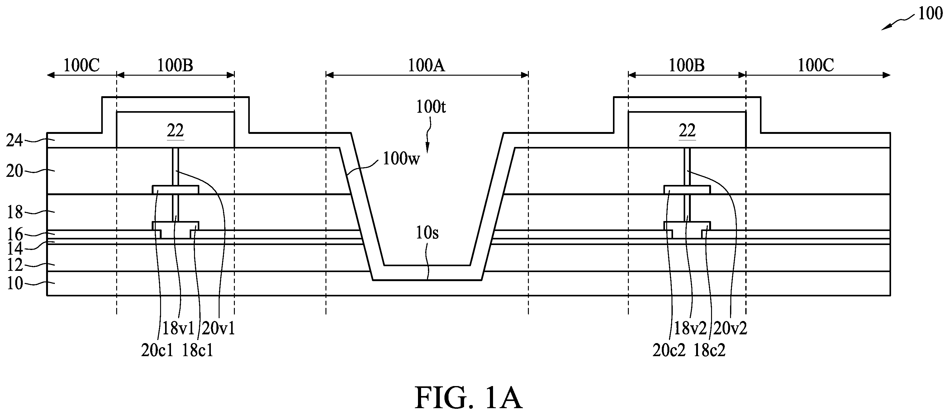
A is a simplified schematic cross-sectional view of a portion of a semiconductor wafer according to certain embodiments of the present disclosure.
B is a simplified schematic cross-sectional view of a portion of a semiconductor wafer according to certain embodiments of the present disclosure.
C is a simplified schematic cross-sectional view of a portion of a semiconductor wafer according to certain embodiments of the present disclosure.
A , B , C , D , E , F , G and H illustrate a method of manufacturing a semiconductor structure according to some embodiments of the present disclosure.
A , B , C , D , E , F , G , H , I- 1 and J- 1 illustrate a method of manufacturing a semiconductor structure according to some embodiments of the present disclosure.
A , B , C , D , E , F , G , H , I- 2 and J- 2 illustrate a method of manufacturing a semiconductor structure according to some embodiments of the present disclosure.
A shows a simplified schematic diagram of a plan view of a portion of a wafer comprising a plurality of semiconductor devices and a pre-dicing trench according to certain embodiments of the present disclosure.
B is a simplified schematic cross-sectional view of a portion of a semiconductor wafer according to certain embodiments of the present disclosure.
C shows a portion of a semiconductor device according to certain embodiments of the present disclosure.
D shows a portion of a semiconductor device according to certain embodiments of the present disclosure.
E shows a portion of a semiconductor device according to certain embodiments of the present disclosure.
A shows a simplified schematic diagram of a plan view of a portion of a wafer comprising a plurality of semiconductor devices and a pre-dicing trench according to certain comparative embodiments of the present disclosure.
B is a simplified schematic cross-sectional view of a portion of a semiconductor wafer according to certain comparative embodiments of the present disclosure.
C shows a portion of a semiconductor device according to certain comparative embodiments of the present disclosure.
PREFERRED EMBODIMENT OF THE PRESENT INVENTION
The following disclosure provides for many different embodiments, or examples, for implementing different features of the provided subject matter. Specific examples of components and arrangements are described below. These are, of course, merely examples and are not intended to be limiting. In the present disclosure, reference to the formation of a first feature over or on a second feature in the description that follows may include embodiments in which the first and second features are formed in direct contact, and may also include embodiments in which additional features may be formed between the first and second features, such that the first and second features may not be in direct contact. In addition, the present disclosure may repeat reference numerals and/or letters in the various examples. This repetition is for the purpose of simplicity and clarity and does not in itself dictate a relationship between the various embodiments and/or configurations discussed.
Embodiments of the present disclosure are discussed in detail below. It should be appreciated, however, that the present disclosure provides many applicable concepts that can be embodied in a wide variety of specific contexts. The specific embodiments discussed are merely illustrative and do not limit the scope of the disclosure.
Direct bandgap materials, such as group III-V compounds, may include, but are not limited to, for example, gallium arsenide (GaAs), indium phosphide (InP), gallium nitride (GaN), indium gallium arsenide (InGaAs), aluminum gallium arsenide (InAlAs), and others.
A is a simplified schematic cross-sectional view of a portion of a semiconductor wafer according to certain embodiments of the present disclosure.
A shows a semiconductor structure 100 according to certain embodiments of the present disclosure. As shown in A , the semiconductor structure 100 includes a substrate 10 , group III-V layers 12 and 14 , dielectric layers 16 , 18 and 20 , a metal layer 22 and a passivation layer 24 . The semiconductor structure 100 further includes a recess 100 t . In some embodiments, the recess 100 t can also be referred to as a trench.
The substrate 10 may include, without limitation, silicon (Si), doped Si, silicon carbide (SiC), germanium silicide (SiGe), gallium arsenide (GaAs), or other semiconductor materials. The substrate 10 may include, without limitation, sapphire, silicon on insulator (SOI), or other suitable materials. In some embodiments, the substrate 10 may further include a doped region (not shown in A ), for example, a p-well, n-well, or the like.
The group III-V layers 12 and 14 can be disposed on the substrate 10 . The group III-V layers 12 and 14 can be stacked on the substrate 10 . In some embodiments, group III-V layers 12 and 14 can be doped group III-V layers. In some embodiments, the semiconductor structure 100 may include more than two group III-V layers. In some embodiments, the semiconductor structure 100 may include only one group III-V layer.
The group III-V layers 12 and 14 may include, without limitation, for example, doped gallium nitride (doped GaN), doped aluminum gallium nitride (doped AlGaN), doped indium gallium nitride (doped InGaN), and other doped III-V compounds. The group III-V layers 12 and 14 may include, without limitation, for example, a p-type dopant, an n-type dopant, or other dopants. In some embodiments, exemplary dopants can include, for example, but are not limited to, magnesium (Mg), zinc (Zn), cadmium (Cd), silicon (Si), germanium (Ge), and the like.
Dielectric layers 16 , 18 and 20 may include, without limitation, for example, an oxide or a nitride, such as silicon nitride (SiN), silicon oxide (SiO 2 ), and the like. The dielectric layers 16 , 18 and 20 can include, for example, without limitation, a composite layer of an oxide and a nitride, such as Al 2 O 3 /SiN, Al 2 O 3 /SiO 2 , AlN/SiN, AlN/SiO 2 , and the like.
In some embodiments, the semiconductor structure 100 may include more than three dielectric layers. In some embodiments, the semiconductor structure 100 may include only one dielectric layer.
The metal layer 22 can be located on the dielectric layer 20 . In some embodiments, the metal layer 22 may include, without limitation, for example, a refractory metal or a compound thereof. For example, the metal layer 22 may include, without limitation, for example niobium (Nb), molybdenum (Mo), tantalum (Ta), tungsten (W), rhenium (Re), titanium (Ti), vanadium (V), chromium (Cr), zirconium (Zr), hafnium (Hf), ruthenium (Ru), osmium (Os), iridium (Ir) and other metals, or compounds of these metals, such as tantalum nitride (TaN), titanium nitride (TiN), and tungsten carbide (WC), etc.
The passivation layer 24 may be disposed on the dielectric layer 20 . The passivation layer 24 may be disposed on the metal layer 22 . The passivation layer 24 may cover at least a portion of the dielectric layer 20 . The passivation layer 24 may cover at least a portion of the metal layer 22 .
Referring to A , the recess 100 t extends from the dielectric layer 20 to the substrate 10 . The passivation layer 24 can be disposed to cover the sidewall 100 w of the recess 100 t . The passivation layer 24 can be disposed to cover a surface 10 s of the substrate 10 .
The semiconductor structure 100 may include one or more contacts. In some embodiments, the semiconductor structure 100 may include a metal contact 18 c 1 disposed within the dielectric layers 16 and 18 . In some embodiments, the semiconductor structure 100 may include a metal contact 18 c 2 disposed within the dielectric layers 16 and 18 . In some embodiments, the semiconductor structure 100 may include a metal contact 20 c 1 disposed within the dielectric layer 20 . In some embodiments, the semiconductor structure 100 may include a metal contact 20 c 2 disposed within the dielectric layer 20 .
The semiconductor structure 100 may include one or more interlayered connection elements. In some embodiments, the semiconductor structure 100 may include an interlayered connection element 18 v 1 electrically connected between the metal contact 18 c 1 and the metal contact 20 c 1 . In some embodiments, the semiconductor structure 100 may include an interlayered connection element 18 v 2 electrically connected between the metal contact 18 c 2 and the metal contact 20 c 2 . In some embodiments, the semiconductor structure 100 may include an interlayered connection element 20 v 1 electrically connected between the metal contact 20 c 1 and the metal layer 22 . In some embodiments, the semiconductor structure 100 may include an interlayered connection element 20 v 2 electrically connected between the metal contact 20 c 2 and the metal layer 22 .
Each of the interlayered connection elements 18 v 1 , 18 v 2 , 20 v 1 and 20 v 2 can be referred to as a via.
Referring to A , the semiconductor structure 100 includes regions 100 A, 100 B and 100 C. The region 100 A can be referred to as a scribe line or a scribe region. The semiconductor structure 100 can be separated or singulated into some semiconductor devices (not denoted in A , which can include structures in region 100 B and 100 C) by cutting/sawing technique along the region 100 A.
The techniques that may be used to cut/saw the semiconductor structure 100 includes, but are not limited to, mechanical cutting or sawing, laser ablation or laser grooving, plasma dicing, wet etching or dry etching of grooves or trenches, and or laser induced cleaving/splitting.
The region 100 B can include a protection structure (e.g. a seal ring). For example, the seal ring can be disposed around integrated circuits (which can be disposed in region 100 C) for protection. For example, when applying cutting technique to the semiconductor structure 100 along the region 100 A, the seal ring in region 100 B can stop the propagation of the crack (which may be rendered from the scribe region 100 A) so as to protect the structure within region 100 C.
The structure, which includes the metal contact 18 c 1 , the interlayered connection element 18 v 1 , the metal contact 20 c 1 , the interlayered connection element 20 v 1 and the metal layer 22 , can have metal, alloy or other suitable material to protect the circuit (for example, internal circuitry within region 100 C) from damage.
The structure, which includes the metal contact 18 c 2 , the interlayered connection element 18 v 2 , the metal contact 20 c 2 , the interlayered connection element 20 v 2 and the metal layer 22 , can have metal, alloy or other suitable material to protect the circuit (for example, internal circuitry within region 100 C) from damage.
The region 100 C can be an area occupied by circuit(s) or integrated circuit(s). The region 100 C can be referred to as an active device area.
A relatively thin portion (not denoted in A ) under the recess 100 t in the region 100 A of the semiconductor structure 100 can save cost. For example, time of cutting/sawing operation on the semiconductor structure 100 can be reduced. For example, power consumed by cutting/sawing operation can be minimized. For example, lifetime of cutting tool(s) (e.g. knife or blade of knife) can be extended.
A relatively thin portion (not denoted in A ) under the recess 100 t in the region 100 A of the semiconductor structure 100 can also prevent cracks or delamination. Singulation process conducted within the recess 100 t does not pass through interlayered interface (for example, an interface between the substrate 10 and the group III-V layer 12 ) and thus cracks or delamination resulting from lattice mismatch can be avoided.
Lattice mismatch between the substrate 10 and the group III-V layer 12 may cause the interface between the substrate 10 and the group III-V layer 12 to be vulnerable when applying cutting technique to the semiconductor structure 100 . The passivation layer 24 , which defines the recess 100 t in the region 100 A, can cover the interface between the substrate 10 and the group III-V layer 12 for protection. Therefore, the yield rate of manufacturing can be improved. For example, propagation of the crack or delamination caused by cutting operation on the interface between the substrate 10 and the passivation layer 24 can be stopped by the passivation layer 24 covering on the sidewall of the substrate 10 and the group III-V layer 12 .
B is a simplified schematic cross-sectional view of a portion of a semiconductor wafer according to certain embodiments of the present disclosure.
B shows a semiconductor structure 100 ′ according to certain embodiments of the present disclosure. As shown in B , the semiconductor structure 100 ′ includes a substrate 10 , group III-V layers 12 and 14 , dielectric layers 16 , 18 and 20 , a metal layer 22 and a passivation layer 24 ′. The semiconductor structure 100 ′ further includes a recess 100 t . In some embodiments, the recess 100 t can also be referred to as a trench.
The semiconductor structure 100 ′ shown in B is similar to the semiconductor structure 100 shown in A , except for that the passivation layer 24 ′ of the semiconductor structure 100 ′ includes an opening 24 h 1 near the bottom of the recess 100 t . The opening 24 h 1 exposes a portion of the bottom of the recess 100 t . The opening 24 h 1 exposes a portion of the substrate 10 . The opening 24 h 1 exposes a portion of a surface 10 s of the substrate 10 .
Referring to B , the passivation layer 24 ′ includes a portion 24 a disposed on the surface 10 s of the substrate 10 . The passivation layer 24 ′ includes a portion 24 b disposed on the surface 10 s of the substrate 10 . The opening 24 h 1 can be defined by the portion 24 a and the portion 24 b.
The semiconductor structure 100 ′ can be cut/saw along the opening 24 h 1 . Cutting/sawing the semiconductor structure 100 ′ along the opening 24 h 1 may bring many benefits. For example, the portion of the substrate 10 exposed by the opening 24 h 1 has a smaller thickness compared to the other portions of the semiconductor structure 100 ′, cutting/sawing the semiconductor structure 100 ′ along the opening 24 h 1 can reduce the cost of the overall manufacturing process.
In addition, cutting/sawing the semiconductor structure 100 ′ along the opening 24 h 1 merely involves cutting/sawing the substrate 10 , which is a single-layered structure. Therefore, cracks or delamination will not be introduced in the manufacturing process.
In some embodiments, the opening 24 h 1 can be utilized as an alignment mark during the pre-dicing procedure of the semiconductor structure 100 ′. In some embodiments, the opening 24 h 1 can increase the accuracy of the pre-dicing procedure. In some embodiments, the opening 24 h 1 can increase the speed of the pre-dicing procedure. In some embodiments, the opening 24 h 1 can improve the yield of the semiconductor structure 100 ′.
Referring now to the dotted circle A shown in B . In some embodiments, the portion 24 a covers a corner 100 r of the recess 100 t . In some embodiments, the portion 24 a covers an interface 10 i between the substrate 10 and the group III-V layer 12 . The portion 24 a can prevent moisture from entering the interface 10 i between the substrate 10 and the group III-V layer 12 . The portion 24 a can prevent pollutants from entering the interface 10 i between the substrate 10 and the group III-V layer 12 . In addition, propagation of the crack or delamination caused by cutting operation on the interface between the substrate 10 and the passivation layer 24 can be stopped by the portion 24 a.
C is a simplified schematic cross-sectional view of a portion of a semiconductor wafer according to certain embodiments of the present disclosure.
C shows a semiconductor structure 100 ″ according to certain embodiments of the present disclosure. As shown in C , the semiconductor structure 100 ″ includes a substrate 10 , group III-V layers 12 and 14 , dielectric layers 16 , 18 and 20 , a metal layer 22 and a passivation layer 24 ″. The semiconductor structure 100 ″ further includes a recess 100 t . In some embodiments, the recess 100 t can also be referred to as a trench.
The semiconductor structure 100 ″ shown in C is similar to the semiconductor structure 100 shown in A , except for that the passivation layer 24 ″ of the semiconductor structure 100 ″ includes an opening 24 h 2 . The opening 24 h 2 exposes a portion of the bottom of the recess 100 t . The opening 24 h 2 exposes a portion of the substrate 10 . The opening 24 h 2 exposes a portion of a surface 10 s of the substrate 10 .
The recess 100 t may include an inclined sidewall 100 w . The sidewall 100 w may include sidewalls 12 w , 14 w , 16 w , 18 w and 20 w . The sidewall 100 w is adjacent to the region 100 B including protection structures. The sidewall 12 w connects the group III-V layer 14 and the substrate 10 . The sidewall 14 w connects the group III-V layer 12 and the dielectric layer 16 . The sidewall 16 w connects the group III-V layer 14 and the dielectric layer 18 . The sidewall 18 w connects the dielectric layer 16 and the dielectric layer 20 . The sidewall 100 w extends from the dielectric layer 20 to the substrate 10 . The sidewall 100 w connects an upper surface 24 s ″ of the passivation layer 24 ″ to a surface 10 s of the substrate 10 .
The recess 100 t may include an inclined sidewall 100 w 2 . The sidewall 100 w 2 may include sidewalls 12 w 2 , 14 w 2 , 16 w 2 , 18 w 2 and 20 w 2 . The sidewall 100 w 2 is adjacent to the region 100 B including protection structures.
The opening 24 h 2 exposes a sidewall 100 w of the recess 100 t . As shown in C , the sidewall 12 w of the group III-V layer 12 is exposed. The sidewall 14 w of the group III-V layer 14 is exposed. The sidewall 16 w of the dielectric layer 16 is exposed. The sidewall 18 w of the dielectric layer 18 is exposed. The sidewall 20 w of the dielectric layer 20 is exposed.
The semiconductor structure 100 ″ can be cut/saw along the recess 100 t . As previously discussed, cutting/sawing the semiconductor structure 100 ″ along the recess 100 t may bring many benefits. In some embodiments, the recess 100 t can be utilized as an alignment mark during the pre-dicing procedure of the semiconductor structure 100 ″. In some embodiments, the recess 100 t can increase the accuracy of the pre-dicing procedure. In some embodiments, the recess 100 t can increase the speed of the pre-dicing procedure. In some embodiments, the recess 100 t can improve the yield of the semiconductor structure 100 ″.
A , B , C , D , E , F , G and H illustrate a method of manufacturing a semiconductor structure according to some embodiments of the present disclosure.
The operations shown in A , B , C , D , E , F , G and H may be utilized to produce a semiconductor structure similar to the semiconductor structure 100 shown in A .
Referring to A , a substrate 10 is provided, and group III-V layers 12 and 14 are disposed on an upper surface of the substrate 10 . Dielectric layers 16 , 18 and 20 are then disposed on an upper surface of the group III-V layer 14 . A patterned photoresist layer 30 is provided (e.g. formed) on the dielectric layer 20 . The patterned photoresist layer 30 defines an opening 30 h . The opening 30 h exposes a portion of the dielectric layer 20 . The opening 30 h exposes a surface 20 s of the dielectric layer 20 .
Referring to B , portions of the substrate 10 , the group III-V layers 12 and 14 and dielectric layers 16 , 18 and 20 are removed and a recess 100 t is formed. Subsequently, the patterned photoresist layer 30 is then removed.
In some embodiments, the recess 100 t can be formed by an etching process. In some embodiments, the recess 100 t may be formed by dry etching, wet etching, or a combination of dry and wet etching. In some embodiments, the recess 100 t may be formed by laser ablation or laser grooving. In some embodiments, the recess 100 t may be formed by any other suitable techniques.
An angle θ exists between the sidewall 100 w and the surface 10 s of the substrate 10 . The angle θ varies depending on the techniques used to form the recess 100 t.
In some embodiments, the angle θ is in a range of 90 degrees to 100 degrees. In some embodiments, the angle θ is in a range of 100 degrees to 110 degrees. In some embodiments, the angle θ is in a range of 110 degrees to 120 degrees. In some embodiments, the angle θ is in a range of 120 degrees to 130 degrees. In some embodiments, the angle θ is in a range of 130 degrees to 140 degrees. In some embodiments, the angle θ is in a range of 140 degrees to 150 degrees. In some embodiments, the angle θ is in a range of 90 degrees to 150 degrees.
Referring to C , a metal layer 22 is formed on the dielectric layer 20 and the recess 100 t . The metal layer 22 covers an upper surface of the dielectric layer 20 . The metal layer 22 covers the sidewall 100 w of the recess 100 t . The metal layer 22 covers the surface 10 s of the substrate 10 .
In some embodiments, the metal layer 22 can be formed by physical vapor deposition (PVD), chemical vapor deposition (CVD), atomic layer deposition (ALD), plating, and/or other suitable deposition steps.
Referring to D , a photoresist layer 31 is provided (e.g. formed) on the metal layer 22 . The photoresist layer 31 can be conformally formed on the metal layer 22 .
Referring to E , a photolithography process is performed to remove specific portions of the photoresist layer 31 in order to form a patterned photoresist layer. After the photolithography process, portions 31 a , 31 b , 31 c and 31 d of the photoresist layer 31 remain.
Among the portions 31 a , 31 b , 31 c and 31 d , the portions 31 a and 31 b are desired while the portions 31 b and 31 c should be removed.
If the portions 31 b and 31 c are not removed, portions of the metal layer 22 that are under the portions 31 b and 31 c cannot be removed in the subsequent procedures and thus will remain in the recess 100 t . The remaining metal layer will be located around the bottom corners of the recess 100 t . The remaining metal layer within the recess 100 t may adversely affect the cutting/sawing procedure of the semiconductor structure. For example, remaining metal layer within the recess 100 t may cause damage to the wafer sawing/dicing machine that is used to cut/saw the wafer through the recess 100 t.
The portions 31 b and 31 c can result from the focus setting of the photolithography equipment used. That is, since the recess 100 t has a depth, if the focus is set according to the top of the recess 100 t , then the photoresist layer 31 at the bottom of the recess 100 t will be out of the range of the focus. On the other hand, if the focus is set according to the bottom of the recess 100 t , the photoresist layer 31 around the top of the recess 100 t will be out of the range of the focus.
In order to produce a patterned photoresist layer that extends from the top to the bottom of a recess, a two-step photolithography process (that is, the operations shown in E and 2 F ) is proposed.
Referring to F , a photolithography process is performed to remove the portions 31 b and 31 c . The remaining portions 31 a and 31 d can be referred to as a patterned photoresist layer 31 ′. In some embodiments, the focus used in the operation shown in E is different from that used in the operation shown in F . In some embodiments, the focus used in the operation shown in E is shorter than that used in the operation shown in F .
In some embodiments, the focus used in the operation shown in E is selected in accordance with the distance between the top of the recess 100 t and the photolithography equipment. In some embodiments, the focus used in the operation shown in F is selected in accordance with the distance between the bottom of the recess 100 t and the photolithography equipment.
Referring to G , a portion of the metal layer 22 is removed. Subsequently, the patterned photoresist layer 31 ′ is removed. The remained portions of the metal layer 22 can also be referred to as a patterned metal layer.
Referring to H , a passivation layer 24 is formed on the metal layer 22 and the recess 100 t . The passivation layer 24 can be formed conformally along the sidewalls of the recess 100 t.
A , B , C , D , E , F , G , H , I- 1 and J- 1 illustrate a method of manufacturing a semiconductor structure according to some embodiments of the present disclosure.
The operations shown in A , B , C , D , E , F , G , H , I- 1 and J- 1 may be utilized to produce a semiconductor structure similar to the semiconductor structure 100 shown in B .
The operation shown in I- 1 can be performed after the operation shown in H . Referring to I- 1 , a patterned photoresist layer 32 is formed on the passivation layer 24 . The patterned photoresist layer 32 includes an opening 32 h 1 near the bottom of the recess 100 t . The opening 32 h 1 exposes a portion of the passivation layer 24 . The opening 32 h 1 exposes a surface 24 s of the passivation layer 24 .
The operation shown in J- 1 can be performed after the operation shown in I- 1 . Referring to J- 1 , a portion of the passivation layer 24 is removed, and then the patterned photoresist layer 32 is removed. The operation shown in J- 1 produces an opening 24 h 1 from the passivation layer 24 . The opening 24 h 1 exposes a portion of the substrate 10 . The opening 24 h 1 exposes a surface 10 s of the substrate 10 .
A , B , C , D , E , F , G , H , I- 2 and J- 2 illustrate a method of manufacturing a semiconductor structure according to some embodiments of the present disclosure.
The operations shown in A , B , C , D , E , F , G , H , I- 2 and J- 2 may be utilized to produce a semiconductor structure similar to the semiconductor structure 100 shown in C .
The operation shown in I- 2 can be performed after the operation shown in H . Referring to I- 2 , a patterned photoresist layer 32 is formed on the passivation layer 24 . The patterned photoresist layer 32 includes an opening 32 h 2 . The opening 32 h 2 exposes a portion of the passivation layer 24 .
The operation shown in J- 2 can be performed after the operation shown in I- 2 . Referring to J- 2 , a portion of the passivation layer 24 is removed, and then the patterned photoresist layer 32 is removed. The operation shown in J- 2 produces an opening 24 h 2 from the passivation layer 24 . The opening 24 h 2 exposes the recess 100 t . The opening 24 h 2 exposes the sidewall 100 w of the recess 100 t . The opening 24 h 2 exposes a portion of the substrate 10 . The opening 24 h 1 exposes a surface 10 s of the substrate 10 .
A shows a simplified schematic diagram of a plan view of a portion of a wafer comprising a plurality of semiconductor devices and a pre-dicing trench according to certain embodiments of the present disclosure.
Referring to A , the wafer 40 includes semiconductor devices 42 d 1 , 42 d 2 , 42 d 3 and 42 d 4 . The semiconductor device 42 d 1 includes a seal ring 42 s 1 surrounding the peripherals of the semiconductor device 42 d 1 . The semiconductor device 42 d 2 includes a seal ring 42 s 2 surrounding the peripherals of the semiconductor device 42 d 2 . The semiconductor device 42 d 3 includes a seal ring 42 s 3 surrounding the peripherals of the semiconductor device 42 d 3 . The semiconductor device 42 d 4 includes a seal ring 42 s 4 surrounding the peripherals of the semiconductor device 42 d 4 .
The recess 100 t is disposed between the semiconductor device 42 d 1 and the semiconductor device 42 d 2 . The recess 100 t is disposed between the semiconductor device 42 d 1 and the semiconductor device 42 d 3 . The recess 100 t is disposed between the semiconductor device 42 d 2 and the semiconductor device 42 d 4 . The recess 100 t is disposed between the semiconductor device 42 d 3 and the semiconductor device 42 d 4 . The semiconductor devices 42 d 1 , 42 d 2 , 42 d 3 and 42 d 4 can be singulated by sawing the wafer 40 along the recess 100 t.
In some embodiments, the recess 100 t has a width of around 40 micrometers (μm). In some embodiments, the region 100 A has a width of around 40 μm.
B is a simplified schematic cross-sectional view of a portion of a semiconductor wafer according to certain embodiments of the present disclosure. The semiconductor structure 100 d of B can be a cross-sectional view of a portion of the wafer 40 along the dotted line A-A′ of A .
C shows a portion of a semiconductor device according to certain embodiments of the present disclosure.
C shows a portion of the semiconductor device 42 d 1 . The semiconductor device 42 d 1 can be singulated from the wafer 40 . In some embodiments, the semiconductor device 42 d 1 can be singulated from the wafer 40 using a metal blade. In some embodiments, the semiconductor device 42 d 1 can be singulated from the wafer 40 using a water-cooled circular saw with diamond-tipped teeth.
Referring to the dotted circle B shown in C , the upper surface 24 s of the passivation layer 24 may not be coplanar with the interface 10 i . Also, the upper surface 10 s of the substrate 10 may not be coplanar with the interface 10 i . As previously discussed in accordance with B , the configuration of the portion 24 a includes several advantages. For example, the portion 24 a can prevent moisture from entering the interface 10 i between the substrate 10 and the group III-V layer 12 . The portion 24 a can prevent pollutants from entering the interface 10 i between the substrate 10 and the group III-V layer 12 . In addition, propagation of the crack or delamination caused by cutting operation on the interface between the substrate 10 and the passivation layer 24 can be stopped by the portion 24 a.
Referring again to the dotted circle B shown in C , the blade or the saw used to singulate the semiconductor device 42 d 1 may pass through the passivation layer 24 and introduce uneven edges to the passivation layer 24 . The blade or the saw used to singulate the semiconductor device 42 d 1 may introduce uneven edges to the substrate 10 .
As shown in the dotted circle B, the passivation layer 24 can have a relatively rough surface 24 w 1 adjacent to the substrate 10 . The passivation layer 24 can have a relatively uneven surface 24 w 1 adjacent to the substrate 10 . The passivation layer 24 can have a relatively rough surface 24 w 1 adjacent to the interface 10 i . The passivation layer 24 can have a relatively uneven surface 24 w 1 adjacent to the interface 10 i . The passivation layer 24 can have a relatively rough surface 24 w 1 facing opposite the interface 10 i . The passivation layer 24 can have a relatively uneven surface 24 w 1 facing opposite the interface 10 i . The passivation layer 24 can have a relatively rough surface 24 w 1 adjacent to the sidewall 100 w . The passivation layer 24 can have an uneven surface 24 w 1 facing opposite the sidewall 100 w . The passivation layer 24 can have a relatively rough surface 24 w 1 facing opposite the sidewall 100 w.
The substrate 10 can have a relatively rough surface 10 w adjacent to the interface 10 i . The substrate 10 can have a relatively uneven surface 10 w adjacent to the interface 10 i . The substrate 10 can have a relatively rough surface 10 w facing opposite/away the interface 10 i . The substrate 10 can have a relatively uneven surface 10 w facing opposite/away the interface 10 i . The substrate 10 can have a relatively rough surface 10 w adjacent to the sidewall 100 w . The substrate 10 can have a relatively uneven surface 10 w facing opposite/away the sidewall 100 w.
D shows a portion of a semiconductor device according to certain embodiments of the present disclosure. D shows a portion of the semiconductor device 42 d 1 ′. The semiconductor device 42 d 1 ′ can be singulated from the wafer 40 .
Referring to the dotted circle C shown in D , the blade or the saw used to singulate the semiconductor device 42 d 1 ′ may introduce uneven edges to the substrate 10 . The blade or the saw used to singulate the semiconductor device 42 d 1 ′ may not pass through the passivation layer 24 and thus may not introduce uneven edges to the passivation layer 24 .
As shown in the dotted circle C, the passivation layer 24 can have a relatively smooth surface 24 w 2 adjacent to the substrate 10 . The passivation layer 24 can have a relatively smooth surface 24 w 2 adjacent to the interface 10 i . The passivation layer 24 can have a relatively smooth surface 24 w 2 facing opposite the interface 10 i . The passivation layer 24 can have a relatively smooth surface 24 w 2 facing opposite the sidewall 100 w.
The substrate 10 can have a relatively rough surface 10 w adjacent to the interface 10 i . The substrate 10 can have a relatively uneven surface 10 w adjacent to the interface 10 i . The substrate 10 can have a relatively rough surface 10 w facing opposite the interface 10 i . The substrate 10 can have a relatively uneven surface 10 w facing opposite the interface 10 i.
E shows a portion of a semiconductor device according to certain embodiments of the present disclosure. E shows a portion of the semiconductor device 42 d 1 ″. The semiconductor device 42 d 1 ″ can be singulated from the wafer 40 .
Referring to the dotted circle D shown in E , the blade or the saw used to singulate the semiconductor device 42 d 1 ′ may introduce uneven edges to the substrate 10 . The substrate 10 can have a relatively rough surface 10 w adjacent to the interface 10 i . The substrate 10 can have a relatively uneven surface 10 w adjacent to the interface 10 i . The substrate 10 can have a relatively rough surface 10 w facing opposite the interface 10 i . The substrate 10 can have a relatively uneven surface 10 w facing opposite the interface 10 i . The substrate 10 can have a relatively rough surface 10 w facing opposite the sidewall 100 w.
A shows a simplified schematic diagram of a plan view of a portion of a wafer comprising a plurality of semiconductor devices and a pre-dicing trench according to certain comparative embodiments of the present disclosure.
Referring to A , the wafer 60 includes semiconductor devices 62 d 1 , 62 d 2 , 62 d 3 and 62 d 4 . The semiconductor device 62 d 1 includes a seal ring 62 s 1 surrounding the peripherals of the semiconductor device 62 d 1 . The semiconductor device 62 d 2 includes a seal ring 62 s 2 surrounding the peripherals of the semiconductor device 62 d 2 . The semiconductor device 62 d 3 includes a seal ring 62 s 3 surrounding the peripherals of the semiconductor device 62 d 3 . The semiconductor device 62 d 4 includes a seal ring 62 s 4 surrounding the peripherals of the semiconductor device 62 d 4 .
A recess 62 t 1 surrounds the peripherals of the seal ring 62 s 1 . A recess 62 t 2 surrounds the peripherals of the seal ring 62 s 2 . A recess 62 t 3 surrounds the peripherals of the seal ring 62 s 3 . A recess 62 t 4 surrounds the peripherals of the seal ring 62 s 4 .
B is a simplified schematic cross-sectional view of a portion of a semiconductor wafer according to certain comparative embodiments of the present disclosure.
B shows a semiconductor structure 200 according to certain comparative embodiments of the present disclosure. The semiconductor structure 200 of B can be a cross-sectional view of a portion of the wafer 60 along the dotted line B-B′ of A .
The semiconductor structure 200 includes regions 200 A, 200 B and 200 C. The region 200 A can be referred to as a scribe line or a scribe region. Semiconductor devices included in the semiconductor structure 200 (not shown) can be separated or singulated by cutting/sawing the semiconductor structure 200 along the region 200 A. The region 200 B is a seal ring, and the region 200 C is an area where the semiconductor devices (not shown) located and can be referred to as an active device area.
The semiconductor structure 200 includes a recess 200 t 1 disposed adjacent to one side of the region 200 A and a recess 200 t 2 disposed adjacent to the other side of the region 200 A.
Referring to the region 200 A of B , this region of the semiconductor structure 200 includes multi-layered structures. Therefore, the blade or the saw used in the singulation process will inevitably pass through several interfaces. For example, cutting/sawing along the region 200 A will pass through the interface 10 i between the substrate 10 and the group III-V layer 12 . Since there is a lattice mismatch between the substrate 10 and the group III-V layer 12 , cutting through the interface 10 i will tend to cause cracks or delamination. In accordance with the embodiments shown in B , a crack 12 c may be formed from the interface 10 i and propagate toward the direction of the regions 200 B and 200 C. The cracks or delamination resulting from cutting/sawing along the region 200 A will adversely affect the yield of the overall manufacturing process.
Referring to both A and 4 B , the recess 62 t 1 shown in A may correspond to the recess 200 t 1 shown in B . The recess 62 t 3 shown in A may correspond to the recess 200 t 2 shown in B . The seal rings 62 s 1 and 62 s 3 shown in A may correspond to the regions 200 B shown in B . The semiconductor devices 62 d 1 and 62 d 3 shown in A may be located in the region 200 C of B .
In some embodiments, the recess 200 t 1 , the region 200 A and the recess 200 t 2 have a total width of around 80 μm. In some embodiments, the recess 200 t 1 , the region 200 A and the recess 200 t 2 have a total width of around 120 μm. In some embodiments, the total width of the recess 200 t 1 , the region 200 A and the recess 200 t 2 is in a range from 80 μm to 120 μm.
Due to the width of the recess 200 t 1 , the region 200 A and the recess 200 t 2 , the effective area used of the wafer 60 shown in A can be less than that of the wafer 40 shown in A . In some embodiments, the effective area used of the wafer 60 can be 30% less than that of the wafer 40 . In some embodiments, the effective area used of the wafer 60 can be upto 40% less than that of the wafer 40 . The effective area used here refers to the percentage of the total area of the wafer occupied by the semiconductor device.
C shows a portion of a semiconductor device according to certain comparative embodiments of the present disclosure.
C shows a portion of the semiconductor device 62 d 1 . The semiconductor device 62 d 1 can be singulated from the wafer 60 . In some embodiments, the semiconductor device 62 d 1 can be singulated from the wafer 60 using a blade, a saw, or laser. Referring to C , the semiconductor device 62 d 1 includes a recess 200 t 1 . The passivation layer 24 may extend toward the recess 200 t 1 and cover the sidewall of the recess 200 t 1 .
As used herein, spatially relative terms, such as “beneath,” “below,” “lower,” “above,” “upper,” “lower,” “left,” “right” and the like, may be used herein for ease of description to describe one element or feature's relationship to another element(s) or feature(s) as illustrated in the figures. The spatially relative terms are intended to encompass different orientations of the device in use or operation in addition to the orientation depicted in the figures. The apparatus may be otherwise oriented (rotated 90 degrees or at other orientations) and the spatially relative descriptors used herein may likewise be interpreted accordingly. It should be understood that when an element is referred to as being “connected to” or “coupled to” another element, it may be directly connected to or coupled to the other element, or intervening elements may be present.
As used herein, the terms “approximately”, “substantially”, “substantial” and “about” are used to describe and account for small variations. When used in conduction with an event or circumstance, the terms can refer to instances in which the event of circumstance occurs precisely as well as instances in which the event or circumstance occurs to a close approximation. As used herein with respect to a given value or range, the term “about” generally means within ±10%, ±5%, ±1%, or ±0.5% of the given value or range. Ranges can be expressed herein as from one endpoint to another endpoint or between two endpoints. All ranges disclosed herein are inclusive of the endpoints, unless specified otherwise. The term “substantially coplanar” can refer to two surfaces within micrometers (μm) of lying along a same plane, such as within 10 μm, within 5 μm, within 1 μm, or within 0.5 μm of lying along the same plane. When referring to numerical values or characteristics as “substantially” the same, the term can refer to the values lying within ±10%, ±5%, ±1%, or ±0.5% of an average of the values.
The foregoing outlines features of several embodiments and detailed aspects of the present disclosure. The embodiments described in the present disclosure may be readily used as a basis for designing or modifying other processes and structures for carrying out the same or similar purposes and/or achieving the same or similar advantages of the embodiments introduced herein. Such equivalent constructions do not depart from the spirit and scope of the present disclosure, and various changes, substitutions, and alterations may be made without departing from the spirit and scope of the present disclosure.
Figures (20)
Citations
This patent cites (15)
- US20070293019
- US20090200568
- US20090278236
- US20100112811
- US20170212423
- US20170256638
- US20180012770
- US20180033695
- US20180138368
- US20180337308
- US20200135564
- US101641776
- US102593076
- US109256375
- US109478584