Word Line Driving Circuit with High Access Efficiency
Abstract
A word line driving circuit includes a first circuit and a second circuit. The first circuit is configured to provide a first word line driving voltage and a second word line driving voltage based on a first control signal, a second control signal, a first bias voltage, a second bias voltage and a base voltage. The second circuit is configured to provide the first control signal and the second control signal based on a third control signal, a fourth control signal, a word line control signal, a reverse word line control signal, the first bias voltage, the second bias voltage and the base voltage. The first bias voltage and the second bias voltage have different levels during the read mode and the program mode for adaptively adjusting the read voltage and the program voltage, thereby improving the data access time.
Claims (10)
1. A word line driving circuit, comprising: a first circuit configured to provide a first word line driving voltage and a second word line driving voltage based on a first control signal, a second control signal, a first bias voltage, a second bias voltage and a base voltage, and comprising: a first transistor, including: a first end coupled to the base voltage; a second end; and a control end coupled to a first reverse control signal associated with the first control signal; a second transistor, including: a first end coupled to the second end of the first transistor; a second end for outputting the first word line driving voltage; and a control end coupled to the first bias voltage; a third transistor, including: a first end coupled to the second end of the second transistor; a second end; and a control end coupled to the second bias voltage; a fourth transistor, including: a first end coupled to the second end of the third transistor; a second end; and a control end coupled to a second reverse control signal associated with the second control signal; a fifth transistor, including: a first end coupled to the base voltage; a second end; and a control end coupled to the control end of the first transistor; a sixth transistor, including: a first end coupled to the second end of the fifth transistor; a second end for outputting the second word line driving voltage; and a control end coupled to the first bias voltage; a seventh transistor, including: a first end coupled to the second end of the sixth transistor; a second end; and a control end coupled to the second bias voltage; an eighth transistor, including: a first end coupled to the second end of the seventh transistor; a second end coupled to the second end of the fourth transistor; and a control end coupled to the control end of the fourth transistor; and a second circuit configured to provide the first control signal and the second control signal based on a word line control signal, a reverse word line control signal, the first bias voltage, the second bias voltage and the base voltage, and comprising: a ninth transistor, including: a first end coupled to the base voltage; a second end; and a control end; a tenth transistor, including: a first end coupled to the second end of the ninth transistor; a second end; and a control end coupled to the first bias voltage; an eleventh transistor, including: a first end coupled to the second end of the tenth transistor; a second end; and a control end coupled to the second bias voltage; a twelfth transistor, including: a first end coupled to the second end of the eleventh transistor; a second end; and a control end coupled to the first word line control signal; a thirteenth transistor, including: a first end coupled to the base voltage; a second end coupled to the control end of the ninth transistor; and a control end coupled to the second end of the ninth transistor; a fourteenth transistor, including: a first end coupled to the second end of the thirteenth transistor; a second end; and a control end coupled to the first bias voltage; a fifteenth transistor, including: a first end coupled to the second end of the fourteenth transistor; a second end; and a control end coupled to the second bias voltage; a sixteenth transistor, including: a first end coupled to the second end of the fifteenth transistor; a second end coupled to the second end of the twelfth transistor; and a control end coupled to the reverse word line control signal, wherein a phase of the word line control signal is opposite to a phase of the reverse word line control signal.
Show 9 dependent claims
2. The word line driving circuit of claim 1 , wherein: the first transistor, the second transistor, the fifth transistor, the sixth transistor, the ninth transistor, the tenth transistor, the thirteenth transistor and the fourteenth transistor have a first doping type; and the third transistor, the fourth transistor, the seventh transistor, the eighth transistor, the eleventh transistor, the twelfth transistor, the fifteenth transistor and the sixteenth transistor have a second doping type which is different from the first doping type.
3. The word line driving circuit of claim 1 , wherein the second circuit further comprises: a first voltage generating circuit configured to provide the first control signal based on a third control signal, a first voltage established on the second end of the tenth transistor and a second voltage established on the second end of the fourteenth transistor, and comprising: a seventeenth transistor, including: a first end coupled between the second end of the ninth transistor and the first end of the tenth transistor; a second end; and a control end coupled to the third control signal; an eighteenth transistor, including: a first end coupled to the second end of the seventeenth transistor; a second end; and a control end coupled to the second voltage; a nineteenth transistor, including: a first end coupled to the first end of the seventeenth transistor; a second end coupled to the second end of the eighteenth transistor; and a control end coupled to the first voltage; and a second voltage generating circuit configured to provide the third control signal based on the first control signal, the first voltage and the second voltage, and comprising: a twentieth transistor, including: a first end coupled between the second end of the thirteenth transistor and the first end of the fourteenth transistor; a second end; and a control end coupled to the first control signal; a twenty-first transistor, including: a first end coupled to the second end of the twentieth transistor; a second end; and a control end coupled to the first voltage; a twenty-second transistor, including: a first end coupled to the first end of the twentieth transistor; a second end coupled to the second end of the twenty-first transistor; and a control end coupled to the second voltage.
4. The word line driving circuit of claim 3 , wherein: the first transistor, the second transistor, the fifth transistor, the sixth transistor, the ninth transistor, the tenth transistor, the thirteenth transistor, the fourteenth transistor, the nineteenth transistor and the twenty-second transistor have a first doping type; and the third transistor, the fourth transistor, the seventh transistor, the eighth transistor, the eleventh transistor, the twelfth transistor, the fifteenth transistor, the sixteenth transistor, the eighteenth transistor, the twentieth transistor and the twenty-first transistor have a second doping type which is different from the first doping type.
5. The word line driving circuit of claim 1 , wherein the second circuit further comprises: a twenty-third transistor configured to provide the second control signal based on a fourth control signal, and including: a first end coupled to the second bias voltage; a second end coupled between the second end of the eleventh transistor and the first end of the twelfth transistor; and a control end coupled to the fourth control signal; and a twenty-fourth transistor configured to provide the fourth control signal based on the second control signal, and including: a first end coupled to the second bias voltage; a second end coupled between the second end of the fifteenth transistor and the first end of the sixteenth transistor; and a control end coupled to the second control signal.
6. The word line driving circuit of claim 5 , wherein: the first transistor, the second transistor, the fifth transistor, the sixth transistor, the ninth transistor, the tenth transistor, the thirteenth transistor, the fourteenth transistor, the twenty-third transistor and the twenty-fourth transistor have a first doping type; and the third transistor, the fourth transistor, the seventh transistor, the eighth transistor, the eleventh transistor, the twelfth transistor, the fifteenth transistor and the sixteenth transistor have a second doping type which is different from the first doping type.
7. The word line driving circuit of claim 1 , wherein the second circuit further comprises: a first logic circuit configured to control an operational mode of the word line driving circuit based on the reverse word line control signal and a select signal, and comprising: a twenty-fifth transistor, including: a first end coupled between the second end of the ninth transistor and the first end of the tenth transistor; a second end; and a control end coupled to the second bias voltage; a twenty-sixth transistor, including: a first end coupled to the second end of the twenty-fifth transistor; a second end coupled to the second end of the twelfth transistor; and a control end; and a first logic gate, including: a first input end for receiving the select signal; a second end for receiving the reverse word line control signal; and a control end coupled to the control end of the twenty-sixth transistor; and a second logic circuit configured to control the operational mode of the word line driving circuit based on the word line control signal and the select signal, and comprising: a twenty-seventh transistor, including: a first end coupled between the second end of the thirteenth transistor and the first end of the fourteenth transistor; a second end; and a control end coupled to the second bias voltage; a twenty-eighth transistor, including: a first end coupled to the second end of the twenty-seventh transistor; a second end coupled to the second end of the sixteenth transistor; and a control end; and a second logic gate, including: a first input end for receiving the select signal; a second end for receiving the word line control signal; and a control end coupled to the control end of the twenty-eighth transistor.
8. The word line driving circuit of claim 1 , wherein: the first transistor further includes a third end coupled to the first end of the first transistor; the second transistor further includes a third end coupled to the first end of the second transistor; the third transistor further includes a third end coupled to a ground voltage; the fourth transistor further includes a third end coupled to the ground voltage; the fifth transistor further includes a third end coupled to the first end of the fifth transistor; the sixth transistor further includes a third end coupled to the first end of the sixth transistor; the seventh transistor further includes a third end coupled to the ground voltage; and the eighth transistor further includes a third end coupled to the ground voltage.
9. The word line driving circuit of claim 1 , wherein: the ninth transistor further includes a third end coupled to the first end of the ninth transistor; the tenth transistor further includes a third end coupled to the first end of the tenth transistor; the eleventh transistor further includes a third end coupled to a ground voltage; the twelfth transistor further includes a third end coupled to the second end of the twelfth transistor; the thirteenth transistor further includes a third end coupled to the first end of the thirteenth transistor; the fourteenth transistor further includes a third end coupled to the first end of the fourteenth transistor; the fifteenth transistor further includes a third end coupled to the ground voltage; and the sixteenth transistor further includes a third end coupled to the second end of the sixteenth transistor.
10. The word line driving circuit of claim 1 , wherein the first circuit further comprises: a first inverter configured to receive the first control signal and output the first reverse control signal having a phase opposite to a phase of the first control signal; and a second inverter configured to receive the second control signal and output the second reverse control signal having a phase opposite to a phase of the second control signal.
Full Description
Show full text →
CROSS REFERENCE TO RELATED APPLICATION
This application claims priority of Taiwan Application No. 110145592 filed on Dec. 7, 2021.
BACKGROUND OF THE INVENTION
1. Field of the Invention
The present invention is related to a word line driving circuit with high access efficiency, and more particularly, to a word line driving circuit with high access efficiency for driving non-volatile memory.
2. Description of the Prior Art
With rapid development in technology and increasing demand in the function of information systems, the speed and accuracy of data access, data transmission, data storage and data display need to be improved. The operation of memory is crucial to the efficiency of information systems.
Modern electronic devices are often required to allow multi-systems to run multiple processes on the data processing system. When receiving multiple access requests associated with different types of data access, a memory access controller needs to arrange the sequence for executing different access requests so that each memory program/read command may be executed accurately without any omission or repetition. Therefore, there is a need for improving the memory efficiency by controlling the data access of the memory.
SUMMARY OF THE INVENTION
The present invention provides a word line driving circuit having a first circuit and a second circuit. The first circuit includes a first to an eighth transistors, and is configured to provide a first word line driving voltage and a second word line driving voltage based on a first control signal, a second control signal, a first bias voltage, a second bias voltage and a base voltage. The second circuit includes a ninth to a sixteenth transistors, and is configured to provide the first control signal and the second control signal based on a word line control signal, a reverse word line control signal, the first bias voltage, the second bias voltage and the base voltage. The first transistor includes a first end coupled to the base voltage, a second end and a control end coupled to a first reverse control signal associated with the first control signal. The second transistor includes a first end coupled to the second end of the first transistor, a second end for outputting the first word line driving voltage and a control end coupled to the first bias voltage. The third transistor includes a first end coupled to the second end of the second transistor, a second end and a control end coupled to the second bias voltage. The fourth transistor includes a first end coupled to the second end of the third transistor, a second end and a control end coupled to a second reverse control signal associated with the second control signal. The fifth transistor includes a first end coupled to the base voltage, a second end and a control end coupled to the control end of the first transistor. The sixth transistor includes a first end coupled to the second end of the fifth transistor, a second end for outputting the second word line driving voltage and a control end coupled to the first bias voltage. The seventh transistor includes a first end coupled to the second end of the sixth transistor, a second end and a control end coupled to the second bias voltage. The eighth transistor includes a first end coupled to the second end of the seventh transistor, a second end coupled to the second end of the fourth transistor and a control end coupled to the control end of the fourth transistor. The ninth transistor includes a first end coupled to the base voltage, a second end and a control end. The tenth transistor includes a first end coupled to the second end of the ninth transistor, a second end and a control end coupled to the first bias voltage. The eleventh transistor includes a first end coupled to the second end of the tenth transistor, a second end and a control end coupled to the second bias voltage. The twelfth transistor includes a first end coupled to the second end of the eleventh transistor, a second end and a control end coupled to the first word line control signal. The thirteenth transistor includes a first end coupled to the base voltage, a second end coupled to the control end of the ninth transistor and a control end coupled to the second end of the ninth transistor. The fourteenth transistor includes a first end coupled to the second end of the thirteenth transistor, a second end and a control end coupled to the first bias voltage. The fifteenth transistor includes a first end coupled to the second end of the fourteenth transistor, a second end and a control end coupled to the second bias voltage. The sixteenth transistor includes a first end coupled to the second end of the fifteenth transistor, a second end coupled to the second end of the twelfth transistor and a control end coupled to the reverse word line control signal, wherein a phase of the word line control signal is opposite to a phase of the reverse word line control signal.
These and other objectives of the present invention will no doubt become obvious to those of ordinary skill in the art after reading the following detailed description of the preferred embodiment that is illustrated in the various figures and drawings.
BRIEF DESCRIPTION OF THE DRAWINGS
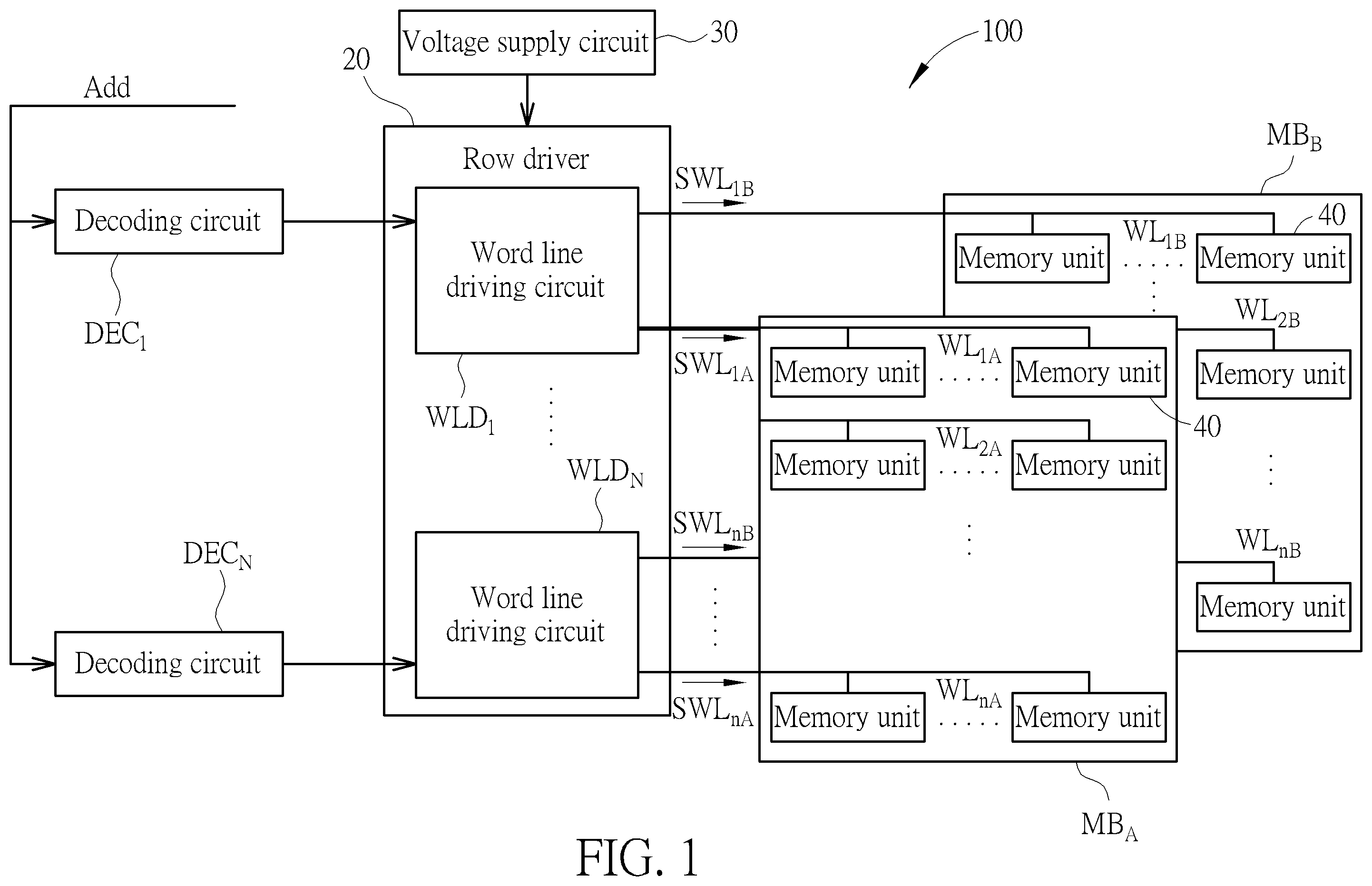
is a diagram illustrating a memory device according to an embodiment of the present invention.
is a functional diagram illustrating each word line driving circuit in a memory device according to an embodiment of the present invention.
is a diagram illustrating an implementation of the first circuit of each word line driving circuit in a memory device according to an embodiment of the present invention.
is a diagram illustrating an implementation of the second circuit of each word line driving circuit in a memory device according to an embodiment of the present invention.
is a diagram illustrating the waveform of a selected word line when each word line driving circuit in the memory device operates in the read mode according to an embodiment of the present invention.
is a diagram illustrating the waveform of an unselected word line when each word line driving circuit in the memory device operates in the read mode according to an embodiment of the present invention.
is a diagram illustrating the waveform of a selected word line when each word line driving circuit in the memory device operates in the program mode according to an embodiment of the present invention.
is a diagram illustrating the waveform of an unselected word line when each word line driving circuit in the memory device operates in the program mode according to an embodiment of the present invention.
DETAILED DESCRIPTION
is a diagram illustrating a memory device 100 according to an embodiment of the present invention. The memory device includes decoding circuits DEC 1 -DEC N , a row driver 20 , a voltage supply circuit 30 , and a plurality of memory blocks, wherein N is a positive integer. For illustrative purpose, depicts two memory blocks MB A and MB B each including a plurality of memory units 40 . However, the number of the memory blocks does not limit the scope of the present invention.
The row driver 20 includes N word line driving circuits WLD 1 -WLD N configured to drive the memory block MB A via word lines WL 1A -WL nA and drive the memory block MB B via word lines WL 1B -WL nB , wherein each word line is coupled to a plurality of memory units 40 and n is a positive integer. Each word line driving circuit is configured to output two word line driving voltages to the memory blocks MB A and MB B for driving the corresponding memory units 40 . More specifically, the word line driving circuit WLD 1 is configured to output a word line driving voltage SWL 1A to the word line WL 1A for driving the memory blocks MB A and output a word line driving voltage SWL 1B to the word line WL 1B for driving the memory blocks MB B . Similarly, the word line driving circuit WLD N is configured to output a word line driving voltage SWL nA to the word line WL nA for driving the memory blocks MB A and output a word line driving voltage SWL nB to the word line WL nB for driving the memory blocks MB B .
The decoding circuits DEC 1 -DEC N are configured to decode a memory address Add for generating the decoding signals associated with the word line driving circuits WLD 1 -WLD N , thereby selecting a corresponding word line driving circuit and a corresponding word line in the row driver 20 . For example, when the memory address Add corresponds to the memory units 40 of the memory block MB A which are coupled to the word line WL 1A , the memory address Add may indicate that the word line driving circuit WLD 1 associated with the memory block MB A should be used to access the memory block MB A . When the memory address Add corresponds to the first row of memory units 40 in the memory block MB A , the memory address Add may indicate that the memory block MB A should be accessed via the word line WL 1A associated with the first row of memory units 40 . The voltage supply circuit 30 is configured to provide the row driver 20 with the operating voltages for performing program, read and erase operations on the memory blocks MB A and MB B .
is a functional diagram illustrating each word line driving circuit in the memory device 100 according to an embodiment of the present invention. Each of the word line driving circuits WLD 1 -WLD N includes a first circuit 51 and a second circuit 52 . In the word line driving circuit WLD 1 , the first circuit 51 is configured to provide word line driving voltages SWL 1A and SWL 1B based on a first control signal CTL 1 _ 1 , a second control signal CTL 2 _ 1 , a first bias voltage biasA, a second bias voltage biasB, a base voltage VP_INT, and a ground voltage GND for driving the corresponding word lines WL 1A and WL 1B ; the second circuit 52 is configured to provide the first control signal CTL 1 _ 1 and the second control signal CTL 2 _ 1 to the first circuit 51 based on a word line control signal WLCTL 1 , the first bias voltage biasA, the second bias voltage biasB, the base voltage VP_INT, the ground voltage GND and a select signal PS. Similarly, in the word line driving circuit WLD N , the first circuit 51 is configured to provide word line driving voltages SW nA and SWL nB based on a first control signal CTL 1 _ n , a second control signal CTL 2 _ n , the first bias voltage biasA, the second bias voltage biasB, the base voltage VP_INT, and the ground voltage GND for driving the corresponding word lines WL nA and WL nB ; the second circuit 52 is configured to provide the first control signal CTL 1 _ n and the second control signal CTL 2 _ n to the first circuit 51 based on a word line control signal WLCTLN, the first bias voltage biasA, the second bias voltage biasB, the base voltage VP_INT, the ground voltage GND and the select signal PS.
is a diagram illustrating an implementation of the first circuit 51 of each word line driving circuit in the memory device 100 according to an embodiment of the present invention. For illustrative purpose, depicts the first circuit 51 of the word line driving circuit WLD 1 , wherein the first circuit 51 is configured to provide the word line driving voltages SWL 1A and SWL 1B for driving the word lines WL 1A and WL 1B in the corresponding memory blocks.
In the embodiment illustrated in , the first circuit 51 includes transistors T 1 -T 8 and invertors INV 1 -INV 2 . The invertor INV 1 includes an input end for receiving the first control signal CTL 1 _ 1 and an output end for providing a first reverse control signal CTL 1 B_ 1 , wherein the phase of the first control signal CTL 1 _ 1 is opposite to the phase of the first reverse control signal CTL 1 B_ 1 . The invertor INV 2 includes an input end for receiving the second control signal CTL 2 _ 1 and an output end for providing a second reverse control signal CTL 2 B_ 1 , wherein the phase of the second control signal CTL 2 _ 1 is opposite to the phase of the second reverse control signal CTL 2 B_ 1 . Meanwhile, the inverter INV 1 is further coupled to the first bias voltage biasA and the base voltage VP_INT and the inverter INV 2 is further coupled to the second bias voltage biasB and the ground voltage GND for preventing over-stress. The transistor T 1 includes a first end coupled to the base voltage VP_INT, a second end, and a control end coupled to the output end of the invertor INV 1 for receiving the first reverse control signal CTL 1 B_ 1 . The transistor T 2 includes a first end coupled to the second end of the transistor T 1 , a second end for outputting the word line driving voltage SWL 1A , and a control end coupled to the first bias voltage biasA. The transistor T 3 includes a first end coupled to the second end of the transistor T 2 , a second end, and a control end coupled to the second bias voltage biasB. The transistor T 4 includes a first end coupled to the second end of the transistor T 3 , a second end coupled to the ground voltage GND, and a control end coupled to the output end of the invertor INV 2 for receiving the second reverse control signal CTL 2 B_ 1 . The transistor T 5 includes a first end coupled to the base voltage VP_INT, a second end, and a control end coupled to the output end of the inverter INV 1 for receiving the first reverse control signal CTL 1 B_ 1 . The transistor T 6 includes a first end coupled to the second end of the transistor T 5 , a second end for outputting the word line driving voltage SWL 1B , and a control end coupled to the first bias voltage biasA. The transistor T 7 includes a first end coupled to the second end of the transistor T 6 , a second end, and a control end coupled to the second bias voltage biasB. The transistor T 8 includes a first end coupled to the second end of the transistor T 7 , a second end coupled to the ground voltage GND, and a control end coupled to the output end of the inverter INV 2 for receiving the second reverse control signal CTL 2 B_ 1 . Furthermore, the first end and a third end of each of the transistors T 1 , T 2 , T 5 and T 6 are coupled to each other, and the third ends of the transistors T 3 , T 4 , T 7 and T 8 are coupled to the ground voltage GND.
In the present invention, the transistors T 1 -T 8 may be field effect transistors (FETs). In an embodiment, the transistors T 1 , T 2 , T 5 and T 6 may be P-type FETs, wherein the first end is a source terminal, the second end is a drain terminal, the third end is a body terminal, and the control end is a gate terminal; the transistors T 3 , T 4 , T 7 and T 8 may be N-type FETs, wherein the first end is a drain terminal, the second end is a source terminal, the third end is a body terminal, and the control end is a gate terminal. However, the type of the transistors T 1 -T 8 does not limit the scope of the present invention.
is a diagram illustrating an implementation of the second circuit 52 of each word line driving circuit in the memory device 100 according to an embodiment of the present invention. For illustrative purpose, depicts the second circuit 52 of the word line driving circuit WLD 1 which includes transistors T 9 -T 28 and logic gates NOR 1 and NOR 2 . The transistor T 9 includes a first end coupled to the base voltage VP_INT, a second end for outputting the first control signal CTL 1 _ 1 , and a control end coupled to the second end of the transistor T 13 . The transistor T 10 includes a first end coupled to the second end of the transistor T 9 , a second end for outputting the first voltage Lvout 1 , and a control end coupled to the first bias voltage biasA. The transistor T 11 includes a first end coupled to the second end of the transistor T 10 , a second end for outputting the second control signal CTL 2 _ 1 , and a control end coupled to the second bias voltage biasB. The transistor T 12 includes a first end coupled to the second end of the transistor T 11 , a second end coupled to the ground voltage GND, and a control end coupled to the word line control signal WLCTL 1 . The transistor T 13 includes a first end coupled to the base voltage VP_INT, a second end for outputting the third control signal CTL 3 _ 1 , and a control end coupled to the second end of the transistor T 9 . The transistor T 14 includes a first end coupled to the second end of the transistor T 13 , a second end for outputting the second voltage Lvout 2 , and a control end coupled to the first bias voltage biasA. The transistor T 15 includes a first end coupled to the second end of the transistor T 14 , a second end for outputting the fourth control signal CTL 4 _ 1 , and a control end coupled to the second bias voltage biasB. The transistor T 16 includes a first end coupled to the second end of the transistor T 15 , a second end coupled to the ground voltage GND, and a control end coupled to a reverse word line control signal WLCTL 1 _B, wherein the phase of the reverse word line control signal WLCTL 1 _B is opposite to the phase of the word line control signal WLCTL 1 . Furthermore, the first end and a third end of each of the transistors T 9 , T 10 , T 13 and T 14 are coupled to each other, and the second end and the third end of each of the transistors T 12 and T 16 are coupled to each other.
In the present invention, the transistors T 9 -T 16 may be FETs. In an embodiment, the transistors T 9 , T 10 , T 13 and T 14 may be P-type FETs, wherein the first end is a source terminal, the second end is a drain terminal, the third end is a body terminal, and the control end is a gate terminal; the transistors T 11 , T 12 , T 15 and T 16 may be N-type FETs, wherein the first end is a drain terminal, the second end is a source terminal, the third end is a body terminal, and the control end is a gate terminal. However, the type of the transistors T 9 -T 16 does not limit the scope of the present invention.
In the second circuit 52 , the transistors T 17 -T 19 form a first voltage generating circuit which is configured to provide the first control signal CTL 1 _ 1 based on the third control signal CTL 3 _ 1 , the first voltage Lvout 1 and the second voltage Lvout 2 . The transistor T 17 includes a first end coupled to the second end of the transistor T 9 , a second end, and a control end coupled to the third control signal CTL 3 _ 1 . The transistor T 18 includes a first end coupled to the second end of the transistor T 17 , a second end coupled to the first bias voltage biasA, and a control end coupled between the second end of the transistor T 14 and the first end of the transistor T 15 for receiving the second voltage Lvout 2 . The transistor T 19 includes a first end coupled to the second end of the transistor T 9 , a second end coupled to the first bias voltage biasA, and a control end coupled between the second end of the transistor T 10 and the first end of the transistor T 11 for receiving the first voltage Lvout 1 .
In the second circuit 52 , the transistor T 23 forms a second voltage generating circuit which is configured to provide the second control signal CTL 2 _ 1 based on the fourth control signal CTL 4 _ 1 . The transistor T 23 includes a first end coupled to the second bias voltage biasB, a second end coupled between the second end of the transistor T 11 and the first end of the transistor T 11 for providing the second control signal CTL 2 _ 1 , and a control end coupled to the fourth control signal CTL 4 _ 1 .
In the second circuit 52 , the transistors T 20 -T 22 form a third voltage generating circuit which is configured to provide the third control signal CTL 3 _ 1 based on the first control signal CTL 1 _ 1 , the first voltage Lvout 1 and the second voltage Lvout 2 . The transistor T 20 includes a first end coupled to the second end of the transistor T 13 , a second end, and a control end coupled to the first control signal CTL 1 _ 1 . The transistor T 21 includes a first end coupled to the second end of the transistor T 20 , a second end coupled to the first bias voltage biasA, and a control end coupled between the second end of the transistor T 10 and the first end of the transistor T 11 for receiving the first voltage Lvout 1 . The transistor T 22 includes a first end coupled to the second end of the transistor T 13 , a second end coupled to the first bias voltage biasA, and a control end coupled between the second end of the transistor T 14 and the first end of the transistor T 15 for receiving the second voltage Lvout 2 .
In the second circuit 52 , the transistor T 24 forms a fourth voltage generating circuit which is configured to provide the fourth control signal CTL 4 _ 1 based on the second control signal CTL 2 _ 1 . The transistor T 24 includes a first end coupled to the second bias voltage biasB, a second end coupled between the second end of the transistor T 15 and the first end of the transistor T 16 for providing the fourth control signal CTL 4 _ 1 , and a control end coupled to the second control signal CTL 2 _ 1 .
In the present invention, the transistors T 17 -T 24 may be FETs. In an embodiment, the transistors T 19 , T 22 , T 23 and T 24 may be P-type FETs, wherein the first end is a source terminal, the second end is a drain terminal, the third end is a body terminal, and the control end is a gate terminal; the transistors T 17 , T 18 , T 20 and T 21 may be N-type FETs, wherein the first end is a drain terminal, the second end is a source terminal, the third end is a body terminal, and the control end is a gate terminal. However, the type of the transistors T 17 -T 24 does not limit the scope of the present invention.
In the second circuit 52 , the transistor T 25 , the transistor T 26 and the logic gate NOR 1 form a first logic circuit which is configured to control the operational mode of each word line driving circuit based on the word line control signal WLCTL 1 _B and the select signal PS. The transistor T 25 includes a first end coupled to the second end of the transistor T 9 , a second end, and a control end coupled to the second bias voltage biasB. The transistor T 26 includes a first end coupled to the second end of the transistor T 25 , a second end coupled to the ground voltage GND, and a control end coupled to the output end of the logic gate NOR 1 . The first input end of the logic gate NOR 1 is coupled to the select signal PS, and the second input end of the logic gate NOR 1 is coupled to the word line control signal WLCTL 1 _B.
In the second circuit 52 , the transistor T 27 , the transistor T 28 and the logic gate NOR 2 form a second logic circuit which is configured to control the operational mode of each word line driving circuit based on the word line control signal WLCTL 1 and the select signal PS. The transistor T 27 includes a first end coupled to the second end of the transistor T 13 , a second end, and a control end coupled to the second bias voltage biasB. The transistor T 28 includes a first end coupled to the second end of the transistor T 27 , a second end coupled to the ground voltage GND, and a control end coupled to the output end of the logic gate NOR 2 . The first input end of the logic gate NOR 2 is coupled to the select signal PS, and the second input end of the logic gate NOR 2 is coupled to the word line control signal WLCTL 1 .
In the present invention, the transistors T 25 -T 28 may be FETs, and the logic gates NOR 1 and NOR 2 may be NOR gates. In an embodiment, the transistors T 25 -T 28 may be N-type FETs, wherein the first end is a drain terminal, the second end is a source terminal, the third end is a body terminal, and the control end is a gate terminal. However, the types of the transistors T 25 -T 28 and the logic gates NOR 1 and NOR 2 do not limit the scope of the present invention.
are diagrams illustrating the waveforms of related signals during the operation of each word line driving circuit in the memory device 100 according to an embodiment of the present invention. is a diagram illustrating the waveform of a selected word line when each word line driving circuit in the memory device 100 operates in the read mode according to an embodiment of the present invention. is a diagram illustrating the waveform of an unselected word line when each word line driving circuit in the memory device 100 operates in the read mode according to an embodiment of the present invention. is a diagram illustrating the waveform of a selected word line when each word line driving circuit in the memory device 100 operates in the program mode according to an embodiment of the present invention. is a diagram illustrating the waveform of an unselected word line when each word line driving circuit in the memory device 100 operates in the program mode according to an embodiment of the present invention.
In the present invention, the transistors T 1 -T 28 are core transistors. Compared to an I/O transistor, a core transistor is characterized in minimized channel length and gate oxide thickness for providing optimized efficiency.
As depicted in , in the read mode, the select signal PS is at a low voltage level (such as 0V), the value of the base voltage VP_INT may be set to the voltage level of core transistor (such as 0.9V), the value of the first bias voltage biasA may be set to a high voltage level (such as 0.9V), and the value of the second bias voltage biasB may be set to the voltage level of core transistor (such as 0.9V). In the program mode, the select signal PS is at a high voltage level (such as 0.9V), the value of the base voltage VP_INT may be set to the voltage level of I/O transistor (such as 1.79V), and the values of the first bias voltage biasA and the second bias voltage biasB may be set to around half the voltage level of core transistor. In an embodiment, the value of the first bias voltage biasA may be set to 0.4*VP_INT (about 0.7V), and the value of the second bias voltage biasB may be set to 0.6*VP_INT (about 1.04V) in the program mode. However, the above-mentioned voltage levels are merely for illustrative purpose and do not limit the scope of the present invention.
In an embodiment, each memory unit 40 in the memory blocks of the memory device 100 may be non-volatile memory (NVM) which includes, but not limited to, read-only memory (ROM), erasable programmable read-only memory (EPROM), electrically-erasable programmable read-only memory (EEPROM), flash EEPROM, non-volatile static random access memory (NVSRAM), ferroelectric random access memory (FeRAM), or eFuse functioning as one-time programmable read-only memory (OTP-ROM). However, the type of the memory device 100 does not limit the scope of the present invention.
In conclusion, the present memory device 100 can provide each word line driving circuit with the first bias voltage biasA and the second bias voltage biasB having different levels during the read mode and the program mode, thereby adaptively adjusting g the read voltage and the program voltage. Therefore, the present invention can protect the memory device from over-drive and improve the data access efficiency.
Those skilled in the art will readily observe that numerous modifications and alterations of the device and method may be made while retaining the teachings of the invention. Accordingly, the above disclosure should be construed as limited only by the metes and bounds of the appended claims.
Figures (8)
Citations
This patent cites (8)
- US20050128858
- US20080232173
- US20110242872
- US20120120751
- US20130148411
- US20170169874
- US20170358344
- US20200098406