Connector Attached Multi-conductor Cable
Abstract
A connector attached multi-conductor cable includes a multi-conductor cable and a connector that includes a circuit board including first to third surfaces. The circuit board includes first pads provided on the first surface and connected to central conductors of wires; second pads provided on the first surface, arranged in a first direction parallel to the third surface, and connected to the first pads; a first ground layer provided between the first and second surfaces, and extending in a second direction parallel to the first surface and perpendicular to the first direction; and a conductive member provided apart from the first pads in the second direction with respect to the second pads, and connected to the first ground layer. The conductive member is positioned on the first surface side with respect to the first ground layer in a third direction perpendicular to the first surface.
Claims (16)
1. A connector attached multi-conductor cable comprising: a multi-conductor cable including a plurality of electric wires; and a connector connected to one end of the multi-conductor cable, wherein the connector includes a circuit board including a first surface, a second surface on a side opposite to the first surface, and a third surface provided at a tip in a direction of connector insertion to connect the first surface to the second surface, wherein the circuit board includes a first group of pads including a plurality of first pads provided on the first surface and connected to central conductors of the electric wires, a second group of pads including a plurality of second pads provided on the first surface, arranged in a first direction parallel to the third surface as viewed from above a top surface of the first surface, and connected to the first pads, a first ground layer provided between the first surface and the second surface, and extending in a second direction parallel to the first surface and perpendicular to the first direction, and a conductive member provided on a side apart from the first group of pads in the second direction with respect to the second group of pads, and connected to the first ground layer, and wherein the conductive member is positioned on the first surface side with respect to the first ground layer in a third direction perpendicular to the first surface.
12. A connector attached multi-conductor cable comprising: a multi-conductor cable including a plurality of coaxial electric wires; and a connector connected to one end of the multi-conductor cable, wherein each of the plurality of coaxial electric wire includes a central conductor, an insulating layer formed on an outer periphery of the central conductor, and an external conductor formed on an outer circumference of the insulating layer, wherein the connector includes a circuit board including a first surface, a second surface on a side opposite to the first surface, and a third surface provided at a tip in a direction of connector insertion to connect the first surface to the second surface, and wherein the circuit board includes a first group of pads including a plurality of first pads provided on the first surface to which the central conductors are connected, a second group of pads including a plurality of second pads provided apart from the first pads and arranged in a first direction parallel to the third surface as viewed from above a top surface of the first surface, and connected to the first pads in the circuit board, a ground layer provided between the first surface and the second surface, and extending in a second direction parallel to the first surface and perpendicular to the first direction, a third pad provided on the first surface on a side apart from the second group of pads in the second direction, and connected to the ground layer, and a fourth pad provided on the first surface, and connected to the ground layer and the external conductor.
Show 14 dependent claims
2. The connector attached multi-conductor cable as claimed in claim 1 , wherein the conductive member includes a second ground layer positioned on the first surface side with respect to the first ground layer in the third direction, and a conductive path connecting the first ground layer and the second ground layer.
3. The connector attached multi-conductor cable as claimed in claim 1 , wherein part of the conductive member is exposed on the first surface.
4. The connector attached multi-conductor cable as claimed in claim 1 , wherein the conductive member includes a third pad for grounding provided on the first surface on a side apart from the first group of pads in the second direction with respect to the second group of pads.
5. The connector attached multi-conductor cable as claimed in claim 4 , wherein the third pad includes a portion arranged in parallel with the plurality of second pads in the first direction.
6. The connector attached multi-conductor cable as claimed in claim 4 , wherein a thickness of the third pad is equal to a thickness of the second plurality of pads.
7. The connector attached multi-conductor cable as claimed in claim 4 , wherein a size of the third pad in the second direction is greater than or equal to 0.5 mm and less than or equal to 2.0 mm.
8. The connector attached multi-conductor cable as claimed claim 1 , wherein the first pads and the second pads are pads for signal transmission.
9. The connector attached multi-conductor cable as claimed in claim 1 , wherein the multi-conductor cable includes a ground conductor, and wherein the circuit board includes a fourth pad provided on the first surface, and connected to the first ground layer and the ground conductor.
10. The connector attached multi-conductor cable as claimed in claim 9 , wherein the electric wire is a coaxial electric wire including an insulating layer formed on an outer circumference of the central conductor, and an external conductor formed on an outer circumference of the insulating layer, and wherein the ground conductor is the external conductor.
11. The connector attached multi-conductor cable as claimed claim 1 , wherein the circuit board includes a plurality of wirings each connected to one of the plurality of first pads, and wherein the one of the plurality of wirings is connected to one of the plurality of second pads.
13. The connector attached multi-conductor cable as claimed in claim 1 , further comprising: a wiring electrically connecting a first pad with a second pad, wherein the wiring is provided between the first ground layer and the first pad in the third direction, and overlaps with the first ground layer as viewed from the first surface.
14. The connector attached multi-conductor cable as claimed in claim 1 , wherein an interval between first pads is greater than an interval between second pads.
15. The connector attached multi-conductor cable as claimed in claim 9 , wherein the electric wire includes a coaxial electric wire including an insulating layer formed on an outer circumference of one of the central conductors, and an insulated electric wire having an external cover formed on an outer circumference of one of the central conductors, wherein the first group of pads includes one first pad connect to the coaxial electric wire, and another first pad connect to the insulated electric wire, and wherein the fourth pad includes two pads provided to have said another first pad interposed in-between in the first direction, and a first connecting pad connecting the two pad.
16. The connector attached multi-conductor cable as claimed in claim 15 , wherein the conductive member includes a third pad for grounding provided on the first surface on a side apart from the first group of pads in the second direction with respect to the second group of pads, wherein the third pad includes two connector pads provided to have a second pad interposed in-between in the first direction, and a second connecting pad connecting the two connector pad, and wherein a length of the first connecting pad is shorter than a length of the second connecting pad in the first direction.
Full Description
Show full text →
TECHNICAL FIELD
The present disclosure relates to a connector attached multi-conductor cable.
The present application claims priority under Japanese Application No. 2020-021343, filed on Feb. 12, 2020, the entire contents of which are hereby incorporated by reference.
BACKGROUND ART
As a connector attached multi-conductor cable used for transmission between electronic devices, a connector attached multi-conductor cable that can be connected to an electronic device regardless of the orientation of the top and bottom of the connector, has been disclosed (Patent Document 1).
RELATED-ART DOCUMENTS
Patent Document
• Patent Document 1: Japanese Laid-Open Patent Application No. 2017-69152
SUMMARY OF INVENTION
Means for Solving Problems
A connector attached multi-conductor cable according to the present disclosure includes a multi-conductor cable including a plurality of electric wires; and a connector connected to one end of the multi-conductor cable, wherein the connector includes a circuit board including a first surface, a second surface on a side opposite to the first surface, and a third surface provided at a tip in a direction of connector insertion to connect the first surface to the second surface, wherein the circuit board includes a first group of pads including a plurality of first pads provided on the first surface and connected to central conductors of the electric wires, a second group of pads including a plurality of second pads provided on the first surface, arranged in a first direction parallel to the third surface as viewed from above a top surface of the first surface, and connected to the first pads, a first ground layer provided between the first surface and the second surface, and extending in a second direction parallel to the first surface and perpendicular to the first direction, and a conductive member provided on a side apart from the first group of pads in the second direction with respect to the second group of pads, and connected to the first ground layer, and wherein the conductive member is positioned on the first surface side with respect to the first ground layer in a third direction perpendicular to the first surface.
BRIEF DESCRIPTION OF DRAWINGS
is a perspective view illustrating a configuration of a connector attached multi-conductor cable according to an embodiment.
is a diagram illustrating an example of pads and connector pads provided on a first circuit board.
is a cross sectional view illustrating an example of a cross sectional structure of the first circuit board.
is a diagram illustrating an example of pads and connector pads provided on a second circuit board.
is a cross sectional view illustrating an example of a cross sectional structure of the second circuit board.
is a cross sectional view illustrating a modified example of the cross sectional structure of the first circuit board.
MODE FOR CARRYING OUT THE INVENTION
Problems to be Solved by the Present Disclosure
According to a multi-conductor cable disclosed in Patent Document 1, although the intended purpose can be achieved, if the frequency of transmitted signals increase, reflection is likely to occur.
The present disclosure has an object to provide a connector attached multi-conductor cable that is capable of reducing reflection of signals.
Effect of the Disclosure
According to the present disclosure, reflection of signals can be reduced.
Embodiments for implementation will be described in the following.
DESCRIPTION OF EMBODIMENTS OF THE PRESENT DISCLOSURES
[1] A connector attached multi-conductor cable according to one aspect in the present disclosure includes a multi-conductor cable including a plurality of electric wires; and a connector connected to one end of the multi-conductor cable, wherein the connector includes a circuit board including a first surface, a second surface on a side opposite to the first surface, and a third surface provided at a tip in a direction of connector insertion to connect the first surface to the second surface, wherein the circuit board includes a first group of pads including a plurality of first pads provided on the first surface and connected to central conductors of the electric wires, a second group of pads including a plurality of second pads provided on the first surface, arranged in a first direction parallel to the third surface as viewed from above a top surface of the first surface, and connected to the first pads, a first ground layer provided between the first surface and the second surface, and extending in a second direction parallel to the first surface and perpendicular to the first direction, and a conductive member provided on a side apart from the first group of pads in the second direction with respect to the second group of pads, and connected to the first ground layer, and wherein the conductive member is positioned on the first surface side with respect to the first ground layer in a third direction perpendicular to the first surface.
The conductive member is provided on the side apart from the first group of pads with respect to the second group of pads in the second direction, connected to the first ground layer, and positioned on the first surface-side with respect to the first ground layer in the third direction. In addition, it is connected to the second group of pads, and the connector pins through which signals are transmitted are provided above the conductive member. Therefore, even in the case where the frequency of signals transmitted via the connector pins is high, for example, even in the case where the frequency is around 20 GHz, unmatching of the differential impedance can be suppressed in the connecting part of the connector pins and the second group of pads, and signal reflection in the vicinity of this connecting part can be suppressed.
[2] In [1], the conductive member may include a second ground layer positioned on the first surface side with respect to the first ground layer in the third direction, and a conductive path connecting the first ground layer and the second ground layer. It becomes easier to position the conductive member on the first surface side with respect to the first ground layer.
[3] In [1] or [2], part of the conductive member may be exposed on the first surface. It becomes easier to suppress unmatching of the differential impedance.
[4] In [1] to [3], the conductive member may include a third pad for grounding provided on the first surface on a side apart from the first group of pads in the second direction with respect to the second group of pads. The third pad facilitates shortening the distance between the connector pins and the conductive member.
[5] In [4], the third pad may include a portion arranged in parallel with the plurality of second pads in the first direction. It becomes easier to hold the electric potential of the third pad to the ground.
[6] In [4] or [5], a thickness of the third pad may be equal to a thickness of the second plurality of pads. It becomes easier to form the third pad simultaneously with the second group of pads.
[7] In [4] to [6], a size of the third pad in the second direction may be greater than or equal to 0.5 mm and less than or equal to 2.0 mm. Reflection can be suppressed appropriately while keeping down the size of the circuit board.
[8] in [1] to [7], the first pads and the second pads may be pads for signal transmission. Reflection of signals transmitted through the first pads and the second pads can be suppressed.
[9] In [1] to [8], the multi-conductor cable may include a ground conductor, and the circuit board includes a fourth pad provided on the first surface, and connected to the first ground layer and the ground conductor. The first ground layer can be easily connected with the ground conductor.
[10] In [9], the electric wire may be a coaxial electric wire including an insulating layer formed on an outer circumference of the central conductor, and an external conductor formed on an outer circumference of the insulating layer, and the ground conductor may be the external conductor. The external conductor of the coaxial electric wire can be used as the ground conductor.
[11] In [1] to [10], the circuit board may include a plurality of wirings each connected to one of the plurality of first pads, and the one of the plurality of wirings may be connected to one of the plurality of second pads. The first pads can be easily connected with the second pads.
[12] A connector attached multi-conductor cable according to another aspect in the present disclosure includes a multi-conductor cable including a plurality of coaxial electric wires; and a connector connected to one end of the multi-conductor cable, wherein each of the plurality of coaxial electric wire includes a central conductor, an insulating layer formed on an outer periphery of the central conductor, and an external conductor formed on an outer circumference of the insulating layer, wherein the connector includes a circuit board including a first surface, a second surface on a side opposite to the first surface, and a third surface provided at a tip in a direction of connector insertion to connect the first surface to the second surface, and wherein the circuit board includes a first group of pads including a plurality of first pads provided on the first surface to which the central conductors are connected, a second group of pads including a plurality of second pads provided apart from the first pads and arranged in a first direction parallel to the third surface as viewed from above a top surface of the first surface, and connected to the first pads in the circuit board, a ground layer provided between the first surface and the second surface, and extending in a second direction parallel to the first surface and perpendicular to the first direction, a third pad provided on the first surface on a side apart from the second group of pads in the second direction, and connected to the ground layer, and a fourth pad provided on the first surface, and connected to the ground layer and the external conductor.
The third pad is provided on a side apart from the first group of pads with respect to the second group of pads in the second direction, connected to the ground layer, and provided on the first surface. In addition, connector pins connected to the second group of pads through which signals are transmitted are provided above the third pad. Therefore, even in the case where the frequency of signals transmitted via the connector pins is high, for example, even in the case where the frequency is around 20 GHz, unmatching of the differential impedance can be suppressed in the connecting part of the connector pins and the second group of pads, and signal reflection in the vicinity of this connecting part can be suppressed.
Details of the Embodiment of the Present Disclosure
In the following, embodiments of the present disclosure will be described in detail with reference to the accompanying drawings; however, the present embodiments are not limited as exemplified. Note that in the present specification and drawings, components having substantially the same functional configurations may be assigned the same reference numerals, to omit duplicated description.
[Configuration of Multi-Conductor Cable]
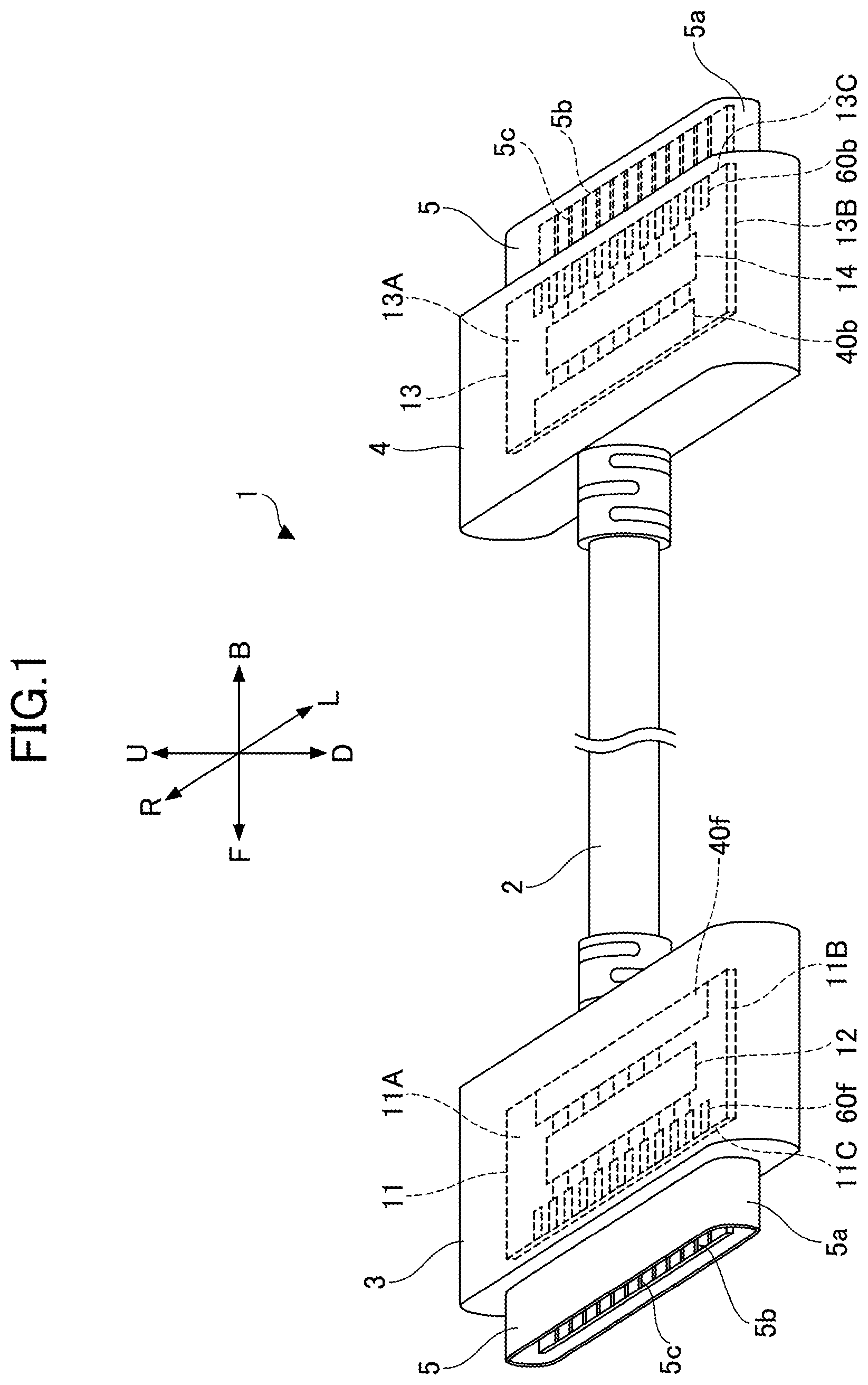
At the outset, a configuration of a connector attached multi-conductor cable according to an embodiment will be described. is a perspective view illustrating a configuration of a connector attached multi-conductor cable according to an embodiment.
The connector attached multi-conductor cable 1 according to the present embodiment can be used, for example, as a cable connecting electronic devices with each other (not illustrated). Note that each of U, D, F, B, R, and L shown in and the like designates a direction with respect to the connector attached multi-conductor cable 1 , where U designates an upward direction, D designates a downward direction, F designates a forward direction, B designates a backward direction, R designates a rightward direction, and L designates a leftward direction. An RL direction is an example of a first direction, an FB direction is an example of a second direction, and a UD direction is an example of a third direction.
As illustrated in , the connector attached multi-conductor cable 1 includes a multi-conductor cable 2 , a first connector 3 , and a second connector 4 . The first connector 3 is attached to one end of the multi-conductor cable 2 on a side in the forward direction F. The second connector 4 is attached to one end of the multi-conductor cable 2 on a side in the backward direction B.
The connector attached multi-conductor cable 1 includes connector plugs 5 each connected to a receptacle of an electronic device (not illustrated), in the forward direction F with respect to the first connector 3 and in the backward direction B with respect to the second connector 4 . A substantially cylindrical metal shell 5 a is provided as a housing for the connector plug 5 . Inside the metal shell 5 a , a pin holding plate 5 b is housed. The pin holding plate 5 b is a member to hold contact pins 5 c to be connected to a receptacle of an electronic device (not illustrated). The contact pins 5 c are held in the pin holding plate 5 b so as to have an arrangement that is connectable to a receptacle of an electronic device even if the orientations of the leftward direction L and the rightward direction R, and of the upward direction U and the downward direction D of the first connector 3 and the second connector 4 are reversed.
The first connector 3 includes a first circuit board 11 in its inside, to which the multi-conductor cable 2 is connected. The first circuit board 11 includes a first surface 11 A, a second surface 11 B, and a third surface 11 C. In the present example, the first surface 11 A is a surface of the first circuit board 11 on a side in the upward direction U; the second surface 11 B is a surface of the first circuit board 11 on a side in the downward direction D; and the third surface 11 C is a surface of the first circuit board 11 on a side in the forward direction F. The first circuit board 11 includes a first circuit 12 , a group of pads 40 f connected to one end of the first circuit 12 on a side in the backward direction B, and a group of connector pads 60 f connected to the other end of the first circuit 12 on a side in the forward direction F. The group of pads 40 f and the group of connector pads 60 f are provided on the first surface 11 A and the second surface 11 B of the first circuit board 11 . For example, the first circuit board 11 has a thickness of between 0.5 mm and 1.0 mm. The first circuit board 11 is formed to have a substantially flat shape.
The second connector 4 includes a second circuit board 13 in its inside, to which the multi-conductor cable 2 is connected. The second circuit board 13 includes a first surface 13 A, a second surface 13 B, and a third surface 13 C. In the present example, the first surface 13 A is a surface of the second circuit board 13 on a side in the upward direction U; the second surface 13 B is a surface of the second circuit board 13 on a side in the downward direction D; and the third surface 13 C is a surface of the second circuit board 13 on a side in the backward direction B. The second circuit board 13 includes a second circuit 14 , a group of pads 40 b connected to one end of the second circuit 14 on a side in the forward direction F, and a group of connector pads 60 b connected to the other end of the second circuit 14 on a side in the backward direction B. The group of pads 40 b and the group of connector pads 60 b are provided on the first surface 13 A and the second surface 13 B of the second circuit board 13 . For example, the second circuit board 13 has a thickness of between 0.5 mm and 1.0 mm. The second circuit board 13 is formed to have a substantially flat shape.
The multi-conductor cable 2 includes multiple high-speed signal lines, for example, four pairs of coaxial electric wires, and multiple, for example, seven electric wires. For example, each pair of coaxial electric wires is constituted with two lines as the pair, to transmit a high-speed differential signal. The coaxial electric wires constituting a pair of coaxial electric wires include a central conductor, an insulating layer, an external conductor, and an external cover, in this order from the center toward the outside. The electric wire is constituted with an insulated electric wire having a central conductor and an external cover. The external conductor is an example of a ground conductor, and includes a shielding electric wire or a shielding layer. The coaxial electric wire facilitates high-speed signal transmission.
Next, pads included in the group of pads 40 f and connector pads included in the group of pads 60 f will be described. is a diagram illustrating an example of pads and connector pads provided on the first circuit board 11 . In , the top surface (the first surface 11 A) of the first circuit board 11 is illustrated as viewed from a side in the upward direction U with respect to the connector attached multi-conductor cable 1 . The pads and the connector pads provided on the bottom surface (the second surface 11 B) of the first circuit board 11 are illustrated to be transparent through the first circuit board 11 .
The group of pads 40 f includes a first surface-side group of pads 40 Af provided on the first surface 11 A, and a second surface-side group of pads 40 Bf provided on the second surface 11 B. The first surface-side group of pads 40 Af includes pads 41 , 42 , 43 , 44 , 45 , 46 , 47 , 48 , 49 , and 50 . The second surface-side group of pads 40 Bf includes pads 51 , 52 , 53 , 54 , 55 , 56 , 57 , 58 , and 59 .
As illustrated in , on the first surface 11 A, the pad 46 is provided in the leftward direction L with respect to the pad 45 ; and the pads 47 , 48 , 49 , and 50 are provided between the pad 45 and the pad 46 , in this order from the rightward direction R toward the leftward direction L. On the first surface 11 A, the pads 41 and 42 are provided in the forward direction F with respect to the pad 45 , and the pads 43 and 44 are provided in the forward direction F with respect to the pad 46 . On the first surface 11 A, a connecting pad 74 connected to the pads 45 and 46 is provided in the backward direction B with respect to the pads 47 to 50 . The connecting pads 74 may be included in the first surface-side group of pads 40 Af.
As illustrated in , on the second surface 11 B, the pad 56 is provided in the leftward direction L with respect to the pad 55 ; and the pads 57 , 58 , and 59 are provided between the pad 55 and the pad 56 , in this order from the rightward direction R toward the leftward direction L. On the second surface 11 B, the pads 51 and 52 are provided in the forward direction F with respect to the pad 55 , and the pads 53 and 54 are provided in the forward direction F with respect to the pad 56 . On the second surface 11 B, a connecting pad 76 connected to the pads 55 and 56 is provided in the backward direction B with respect to the pads 57 to 59 . The connecting pads 76 may be included in the second surface-side group of pads 40 Bf.
The first surface-side group of pads 40 Af and the second surface-side group of pads 40 Bf are connected to the end of the multi-conductor cable 2 on a side in the forward direction F.
The respective central conductors of one pair of coaxial electric wires among the four pairs of coaxial electric wires included in the multi-conductor cable 2 are connected to the pads 41 and 42 of the first surface 11 A. The respective external conductors of the pair of coaxial electric wires are connected to the pad 45 . The respective central conductors of another pair of coaxial electric wires are connected to the pads 43 and 44 of the first surface 11 A. The respective external conductors of the pair of coaxial electric wires are connected to the pad 46 . The respective central conductors of another pair of coaxial electric wires are connected to the pads 51 and 52 of the second surface 11 B. The respective external conductors of the pair of coaxial electric wires are connected to the pad 55 . The respective central conductors of another pair of coaxial electric wires are connected to the pads 53 and 54 of the second surface 11 B. The respective external conductors of the pair of coaxial electric wires are connected to the pad 56 .
One of the seven electric wires included in the multi-conductor cable 2 is connected to the pad 47 on the first surface 11 A. Another electric wire is connected to the pad 48 on the first surface 11 A. Another electric wire is connected to the pad 49 on the first surface 11 A. Another electric wire is connected to the pad 50 on the first surface 11 A. Another electric wire is connected to the pad 57 on the second surface 11 B. Another electric wire is connected to the pad 58 on the second surface 11 B. Another electric wire is connected to the pad 59 on the second surface 11 B.
The pads 41 to 44 and 47 to 50 are examples of first pads, and the pads 41 to 44 and the pads 47 to 50 are included in a first group of pads 71 Af. The pads 45 and 46 constitute an example of a fourth pad. The pads 51 to 54 and 57 to 59 are examples of first pads, and the pads 51 to 54 and the pads 57 to 59 are included in a first group of pads 71 Bf. The pads 55 and 56 constitute an example of a fourth pad.
The group of connector pads 60 f includes a first surface-side group of connector pads 60 Af provided on the first surface 11 A, and a second surface-side group of connector pads 60 Bf provided on the second surface 11 B. The first surface-side group of connector pads 60 Af includes connector pads A 1 , A 2 , A 3 , A 4 , A 5 , A 6 , A 7 , A 8 , A 9 , A 10 , A 11 , and A 12 . The connector pads A 1 to A 12 of the first surface-side connector pads group 60 Af are arranged in a row in this order from the leftward direction L toward the rightward direction R on the first surface 11 A. In other words, the connector pads A 1 to A 12 are arranged in the RL direction parallel to the third surface 11 C as viewed from above the top surface of the first surface 11 A. The second surface-side group of connector pads 60 Bf includes connector pads B 1 , B 2 , B 3 , B 4 , B 5 , B 6 , B 7 , B 8 , B 9 , B 10 , B 11 , and B 12 . The connector pads B 1 to B 12 of the second surface-side connector pads group 60 Bf are arranged in a row in this order from the rightward direction R toward the leftward direction L on the second surface 11 B. In other words, the connector pads B 1 to B 12 are arranged in the RL direction parallel to the third surface 11 C as viewed from above the top surface of the second surface 11 B. On the first surface 11 A, a connecting pad 73 connected to the connector pads A 1 and A 12 is provided in the forward direction F with respect to the connector pads A 2 to A 11 . On the second surface 11 B, a connecting pad 75 connected to the connector pads B 1 and B 12 is provided in the forward direction F with respect to the connector pads B 2 to B 11 . The connecting pads 73 may be included in the first surface-side group of connector pads 60 Af. The connecting pads 75 may be included in the second surface-side group of connector pads 60 Bf.
The connector pads A 1 and A 12 are ground terminals (GND) for grounding. The connector pads A 2 and A 3 are terminals (TX 1 +, TX 1 −) for high-speed signal transmission. The connector pads A 4 and A 9 are terminals (VBUS) for feeding power to a bus. The connector pad A 5 is a configuration channel (CC) terminal. The connector pads A 6 and A 7 are terminals (D+, D−) for data signals. The connector pad A 8 is a terminal (SBU 1 ) for a side band. The connector pads A 10 and A 11 are terminals (RX 2 +, RX 2 −) for receiving high-speed signals.
The connector pads B 1 and B 12 are ground terminals (GND) for grounding. The connector pads B 2 and B 3 are terminals (TX 2 +, TX 2 −) for high-speed signal transmission. The connector pads B 4 and B 9 are terminals (VBUS) for feeding power to a bus. The connector pad B 5 is a terminal (VCONN) for power supply connection. The connector pad B 8 is a terminal (SBU 2 ) for a side band. The connector pads B 10 and B 11 are terminals (RX 1 +, RX 1 −) for receiving high-speed signals.
The connector pads A 2 to A 11 are examples of second pads, and the connector pads A 2 to A 11 are included in the second group of pads 72 Af. The connecting pad 73 is an example of a third pad, and the connector pads A 1 and A 12 are portions of the third pad. The connector pads B 2 to B 11 are examples of second pads, and the connector pads B 2 to B 11 are included in the second group of pads 72 Bf. The connecting pad 75 is an example of a third pad, and the connector pads B 1 and B 12 are portions of the third pad.
The first surface-side group of pads 40 Af and the second surface-side group of pads 40 Bf are connected by the first circuit 12 to the first surface-side group of connector pads 60 Af and the second surface-side group of connector pads 60 Bf of the first circuit board 11 .
Here, an example of a cross sectional structure of the first circuit board 11 will be described. is a cross sectional view illustrating an example of a cross sectional structure of the first circuit board 11 . corresponds to a cross sectional view along a line in .
As illustrated in , the first circuit board 11 includes five laminated insulating layers 111 , 112 , 113 , 114 , and 115 . The insulating layer 112 is provided in the upward direction U with respect to the insulating layer 111 ; the insulating layer 113 is provided in the upward direction U with respect to the insulating layer 112 ; the insulating layer 114 is provided in the upward direction U with respect to the insulating layer 113 ; and the insulating layer 115 is provided in the upward direction U with respect to the insulating layer 114 . The first circuit board 11 further includes a wiring layer 121 on a bottom surface 111 B of the insulating layer 111 ; a wiring layer 122 on a bottom surface 112 B of the insulating layer 112 ; a wiring layer 123 on a bottom surface 113 B of the insulating layer 113 ; a wiring layer 124 on a top surface 113 A of the insulating layer 113 ; a wiring layer 125 on a top surface 114 A of the insulating layer 114 ; and a wiring layer 126 on a top surface 115 A of the insulating layer 115 . The top surface 115 A of the insulating layer 115 corresponds to the first surface 11 A of the first circuit board 11 , and the bottom surface 111 B of the insulating layer 111 corresponds to the second surface 11 B of the first circuit board 11 . As the material of the insulating layers 111 to 115 , for example, epoxy glass, fluororesin, or the like may be used. Each of the insulating layers 111 to 115 has a thickness of, for example, greater than or equal to 50 μm and less than or equal to 300 μm. As the material of the insulating layers 121 to 126 , for example, copper (Cu) or the like may be used. Each of the insulating layers 121 to 126 has a thickness of, for example, greater than or equal to 10 μm and less than or equal to 100 μm.
The wiring layer 126 includes the first surface-side group of pads 40 Af and the first surface-side group of connector pads 60 Af. The wiring layer 125 includes multiple wirings 125 A, a ground layer 125 B, and a ground layer 125 C. Each of the multiple wirings 125 A is connected to one of the pads 41 to 44 and the pads 47 to 50 . Each of the multiple wirings 125 A is connected to one of the connector pads A 2 to A 11 . The ground layer 125 B is provided in the downward direction D with respect to the connector pad A 1 , in the downward direction D with respect to the connector pad A 12 , and in the downward direction D with respect to the connecting pad 73 . The ground layer 125 C is provided in the downward direction D with respect to the pad 45 , in the downward direction D with respect to the pad 46 , and in the downward direction D with respect to the connecting pad 74 . In the insulating layer 115 , conductive vias 81 each connecting one of the wirings 125 A to one of the pads 41 to 44 and pads 47 to 50 , and conductive vias 82 each connecting one of the wiring 125 A to one of the connector pads A 2 to A 11 are provided. In the insulating layer 115 , a conductive via 83 connecting the connector pad A 1 , the connector pad A 12 , and the connecting pad 73 with the ground layer 125 B is provided. In the insulating layer 115 , a conductive via 84 connecting the pad 45 , the pad 46 , and the connecting pad 74 with the ground layer 125 C is provided.
The wiring layer 124 includes a ground layer 124 A extending in the FB direction. In the insulating layer 114 , a conductive via 85 connecting the ground layer 124 A and ground layer 125 B, and a conductive via 86 connecting the ground layer 124 A and the ground layer 125 C are provided.
The connector pad A 1 , the connector pad A 12 , and the connecting pad 73 may be integrally formed with the conductive via 83 ; and the pad 45 , the pad 46 , and the connecting pad 74 may be integrally formed with the conductive via 84 . Each of the connector pads A 2 to A 11 may be integrally formed with one of the conductive vias 82 ; and each of the pads 41 to 44 and the pads 47 to 50 may be integrally formed with one of the conductive vias 81 . The ground layer 125 B may be integrally formed with the conductive via 85 ; and the ground layer 125 C may be integrally formed with the conductive via 86 .
The wiring layer 124 is an example of a first ground layer; the ground layer 125 B is an example of a second ground layer; and the conductive via 85 is an example of a conductive path. The connecting pad 73 , the conductive via 83 , the ground layer 125 B, and the conductive via 85 are included in a conductive member 131 .
The wiring layer 121 includes the second surface-side group of pads 40 Bf and the second surface-side group of connector pads 60 Bf. The wiring layer 122 includes multiple wirings 122 A, a ground layer 122 B, and a ground layer 122 C. Each of the multiple wirings 122 A is connected to one of the pads 51 to 54 and the pads 57 to 59 . Each of the multiple wirings 122 A is connected to one of the connector pads B 2 to B 11 . The ground layer 122 B is provided in the upward direction U with respect to the connector pad B 1 , in the upward direction U with respect to the connector pad B 12 , and in the upward direction U with respect to the connecting pad 75 . The ground layer 122 C is provided in the upward direction U with respect to the pad 55 , in the upward direction U with respect to the pad 56 , and in the upward direction U with respect to the connecting pad 76 . In the insulating layer 111 , conductive vias 91 each connecting one of the wirings 122 A to one of the pads 51 to 54 and pads 57 to 59 , and conductive vias 92 each connecting one of the wiring 122 A to one of the connector pads B 2 to B 11 are provided. In the insulating layer 111 , a conductive via 93 connecting the connector pad B 1 , the connector pad B 12 , and the connecting pad 75 with the ground layer 122 B is provided. In the insulating layer 111 , a conductive via 94 connecting the pad 55 , the pad 56 , and the connecting pad 76 with the ground layer 122 C is provided.
The wiring layer 123 includes a ground layer 123 A extending in the FB direction. In the insulating layer 112 , a conductive via 95 connecting the ground layer 123 A and ground layer 122 B, and a conductive via 96 connecting the ground layer 123 A and the ground layer 122 C are provided.
The connector pad B 1 , the connector pad B 12 , and the connecting pad 75 may be integrally formed with the conductive via 93 ; and the pad 55 , the pad 56 , and the connecting pad 76 may be integrally formed with the conductive via 94 . Each of the connector pads B 2 to B 11 may be integrally formed with one of the conductive vias 92 ; and each of the pads 51 to 54 and the pads 57 to 59 may be integrally formed with one of the conductive vias 91 . The ground layer 122 B may be integrally formed with the conductive via 95 ; and the ground layer 122 C may be integrally formed with the conductive via 96 .
The wiring layer 123 is an example of a first ground layer; the ground layer 122 B is an example of a second ground layer; and the conductive via 95 is an example of a conductive path. The connecting pad 75 , the conductive via 93 , the ground layer 122 B, and the conductive via 95 are included in a conductive member 132 .
In the example illustrated in , the wiring 125 A is connected to the connector pad A 11 and the pad 41 , and the wiring 122 A is connected to the connector pad B 2 and the pad 51 . In this example, although the wirings connecting the pads to the connector pads are provided only in the wiring layers 122 and 125 , the wirings may also pass through the other wiring layers. Also, a pad on the first surface 11 A may be connected to a connector pad on the second surface 11 B, and a pad on the second surface 11 B may be connected to a connector pad on the first surface 11 A.
As illustrated in , each of the connector pads A 1 to A 12 and the connector pads B 1 to B 12 is connected with one of the connector pins 31 provided in the connector plug 5 . The connector pins 31 are arranged so as to extend in the FB direction. Therefore, the connector pins 31 intersect the connecting pad 73 as viewed from a side in the upward direction U, or intersect the connecting pad 75 as viewed from a side in the downward direction D. The pads 41 to 44 and the pads 51 to 54 are connected with central conductors 33 of coaxial electric wires 32 of the multi-conductor cable 2 . The pads 45 , 46 , 55 , and 56 are connected with external conductors 34 of the coaxial electric wires 32 . In other words, the pads 41 to 44 and 51 to 54 are pads for signal transmission, and the pads 45 , 46 , 55 , and 56 are pads for grounding. Each of the pads 41 to 44 and 51 to 54 is connected to one of the connector pads A 2 , A 3 , A 10 , A 11 , B 2 , B 3 , B 10 , and B 11 that are terminals for high-speed signal transmission (TX 1 +, TX 1 −, TX 2 +, TX 2 −) or terminals for high-speed signal reception (RX 1 +, RX 1 −, RX 2 +, RX 2 −). For example, the pad 41 is connected to the connector pad A 11 ; the pad 42 is connected to the connector pad A 10 ; the pad 43 is connected to the connector pad A 3 ; and the pad 44 is connected to the connector pad A 2 . For example, the pad 51 is connected to the connector pad B 2 ; the pad 52 is connected to the connector pad B 3 ; the pad 53 is connected to the connector pad B 10 ; and the pad 54 is connected to the connector pad B 11 .
Next, pads included in the group of pads 40 b and connector pads included in the group of pads 60 b will be described. is a diagram illustrating an example of pads and connector pads provided on a second circuit board 13 . In , the top surface (the first surface 13 A) of the second circuit board 13 is illustrated as viewed from a side in the upward direction U with respect to the connector attached multi-conductor cable 1 . The pads and the connector pads provided on the bottom surface (the second surface 13 B) of the second circuit board 13 are illustrated to be transparent through the second circuit board 13 .
The group of pads 40 b includes a first surface-side group of pads 40 Ab provided on the first surface 13 A, and a second surface-side group of pads 40 Bb provided on the second surface 13 B. The first surface-side group of pads 40 Ab includes the pads 41 to 50 , like the first surface-side group of pads 40 Af. The second surface-side group of pads 40 Bb includes the pads 51 to 59 , like the second surface-side group of pads 40 Bf.
As illustrated in , on the first surface 13 A, the pad 46 is provided in the rightward direction R with respect to the pad 45 ; and the pads 47 , 48 , 49 , and 50 are provided between the pad 45 and the pad 46 , in this order from the leftward direction L toward the rightward direction R. On the first surface 13 A, the pads 41 and 42 are provided in the backward direction B with respect to the pad 45 , and the pads 43 and 44 are provided in the backward direction B with respect to the pad 46 . On the first surface 13 A, a connecting pad 74 connected to the pads 45 and 46 is provided in the forward direction F with respect to the pads 47 to 50 . The connecting pads 74 may be included in the first surface-side group of pads 40 Ab.
As illustrated in , on the second surface 13 B, the pad 56 is provided in the rightward direction R with respect to the pad 55 ; and the pads 57 , 58 , and 59 are provided between the pad 55 and the pad 56 , in this order from the leftward direction L toward the rightward direction R. On the second surface 13 B, the pads 51 and 52 are provided in the backward direction B with respect to the pad 55 , and the pads 53 and 54 are provided in the backward direction B with respect to the pad 56 . On the second surface 13 B, a connecting pad 76 connected to the pads 55 and 56 is provided in the forward direction F with respect to the pads 57 to 59 . The connecting pads 76 may be included in the second surface-side group of pads 40 Bb.
The first surface-side group of pads 40 Ab and the second surface-side group of pads 40 Bb are connected to the end of the multi-conductor cable 2 on a side in the backward direction B.
The respective central conductors of one pair of coaxial electric wires among the four pairs of coaxial electric wires included in the multi-conductor cable 2 are connected to the pads 41 and 42 of the first surface 13 A. The respective external conductors of the pair of coaxial electric wires are connected to the pad 45 . The respective central conductors of another pair of coaxial electric wires are connected to the pads 43 and 44 of the first surface 13 A. The respective external conductors of the pair of coaxial electric wires are connected to the pad 46 . The respective central conductors of another pair of coaxial electric wires are connected to the pads 51 and 52 of the second surface 13 B. The respective external conductors of the pair of coaxial electric wires are connected to the pad 55 . The respective central conductors of another pair of coaxial electric wires are connected to the pads 53 and 54 of the second surface 13 B. The respective external conductors of the pair of coaxial electric wires are connected to the pad 56 .
One of the seven electric wires included in the multi-conductor cable 2 is connected to the pad 47 on the first surface 13 A. Another electric wire is connected to the pad 48 on the first surface 13 A. Another electric wire is connected to the pad 49 on the first surface 13 A. Another electric wire is connected to the pad 50 on the first surface 13 A. Another electric wire is connected to the pad 57 on the second surface 13 B. Another electric wire is connected to the pad 58 on the second surface 13 B. Another electric wire is connected to the pad 59 on the second surface 13 B.
The pads 41 to 44 and 47 to 50 are examples of first pads, and the pads 41 to 44 and the pads 47 to 50 are included in a first group of pads 71 Ab. The pads 45 and 46 constitute an example of a fourth pad. The pads 51 to 54 and 57 to 59 are examples of first pads, and the pads 51 to 54 and the pads 57 to 59 are included in a first group of pads 71 Bb. The pads 55 and 56 constitute an example of a fourth pad.
The group of pads 60 b includes a first surface-side group of pads 60 Ab provided on the first surface 13 A, and a second surface-side group of pads 60 Bb provided on the second surface 13 B. The first surface-side group of connector pads 60 Ab includes the connector pads A 1 to A 12 , like the first surface-side group of connector pads 60 Af. The connector pads A 1 to A 12 of the first surface-side connector pads group 60 Ab are arranged in a row in this order from the rightward direction R toward the leftward direction L on the first surface 13 A. In other words, the connector pads A 1 to A 12 are arranged in the RL direction parallel to the third surface 13 C as viewed from above the top surface of the first surface 13 A. The second surface-side group of connector pads 60 Bb includes the connector pads B 1 to B 12 , like the second surface-side group of connector pads 60 Bf. The connector pads B 1 to B 12 of the second surface-side connector pads group 60 Bb are arranged in a row in this order from the leftward direction L toward the rightward direction R on the second surface 13 B. In other words, the connector pads B 1 to B 12 are arranged in the RL direction parallel to the third surface 13 C as viewed from above the top surface of the second surface 13 B. On the first surface 13 A, a connecting pad 73 connected to the connector pads A 1 and A 12 is provided in the backward direction B with respect to the connector pads A 2 to A 11 . On the second surface 13 B, a connecting pad 75 connected to the connector pads B 1 and B 12 is provided in the backward direction B with respect to the connector pads B 2 to B 11 . The connecting pads 73 may be included in the first surface-side group of connector pads 60 Ab. The connecting pads 75 may be included in the second surface-side group of connector pads 60 Bb.
The connector pads A 1 and A 12 are ground terminals (GND) for grounding. The connector pads A 2 and A 3 are terminals (TX 1 +, TX 1 −) for high-speed signal transmission. The connector pads A 4 and A 9 are terminals (VBUS) for feeding power to a bus. The connector pad A 5 is a configuration channel (CC) terminal. The connector pads A 6 and A 7 are terminals (D+, D−) for data signals. The connector pad A 8 is a terminal (SBU 1 ) for a side band. The connector pads A 10 and A 11 are terminals (RX 2 +, RX 2 −) for receiving high-speed signals.
The connector pads B 1 and B 12 are ground terminals (GND) for grounding. The connector pads B 2 and B 3 are terminals (TX 2 +, TX 2 −) for high-speed signal transmission. The connector pads B 4 and B 9 are terminals (VBUS) for feeding power to a bus. The connector pad B 5 is a terminal (VCONN) for power supply connection. The connector pad B 8 is a terminal (SBU 2 ) for a side band. The connector pads B 10 and B 11 are terminals (RX 1 +, RX 1 −) for receiving high-speed signals.
The connector pads A 2 to A 11 are examples of second pads, and the connector pads A 2 to A 11 are included in the second group of pads 72 Ab. The connecting pad 73 is an example of a third pad, and the connector pads A 1 and A 12 are portions of the third pad. The connector pads B 2 to B 11 are examples of second pads, and the connector pads B 2 to B 11 are included in the second group of pads 72 Bb. The connecting pad 75 is an example of a third pad, and the connector pads B 1 and B 12 are portions of the third pad.
The first surface-side group of pads 40 Ab and the second surface-side group of pads 40 Bb are connected by the second circuit 14 to the first surface-side group of connector pads 60 Ab and the second surface-side group of connector pads 60 Bb of the second circuit board 13 .
Here, an example of a cross sectional structure of the second circuit board 13 will be described. is a cross sectional view illustrating an example of a cross sectional structure of the second circuit board 13 . corresponds to a cross sectional view along a line V-V in .
As illustrated in , the second circuit board 13 includes five laminated insulating layers 111 to 115 , like the first circuit board 11 . The second circuit board 13 further includes wiring layers 121 to 125 , like the first circuit board 11 . The top surface 115 A of the insulating layer 115 corresponds to the first surface 13 A of the second circuit board 13 , and the bottom surface 111 B of the insulating layer 111 corresponds to the second surface 13 B of the second circuit board 13 .
The wiring layer 126 includes the first surface-side group of pads 40 Ab and the first surface-side group of connector pads 60 Ab. The wiring layer 125 includes multiple wirings 125 A, a ground layer 125 B, and a ground layer 125 C, like the first circuit board 11 . In the insulating layer 115 , conductive vias 81 to 84 are provided, like the first circuit board 11 . The wiring layer 124 includes a ground layer 124 A extending in the FB direction, like the first circuit board 11 . In the insulating layer 114 , conductive vias 85 to 86 are provided, like the first circuit board 11 .
The wiring layer 121 includes the second surface-side group of pads 40 Bb and the second surface-side group of connector pads 60 Bb. The wiring layer 122 includes multiple wirings 122 A, a ground layer 122 B, and a ground layer 122 C, like the first circuit board 11 . In the insulating layer 111 , conductive vias 91 to 94 are provided, like the first circuit board 11 . The wiring layer 123 includes a ground layer 123 A extending in the FB direction, like the first circuit board 11 . In the insulating layer 112 , conductive vias 95 and 96 are provided, like the first circuit board 11 .
In the example illustrated in , the wiring 125 A is connected to the connector pad A 2 and the pad 44 , and the wiring 122 A is connected to the connector pad B 11 and the pad 54 . In this example, although the wirings connecting the pads to the connector pads are provided only in the wiring layers 122 and 125 , the wirings may also pass through the other wiring layers. Also, a pad on the first surface 13 A may be connected to a connector pad on the second surface 13 B, and a pad on the second surface 13 B may be connected to a connector pad on the first surface 13 A.
As illustrated in , each of the connector pads A 1 to A 12 and the connector pads B 1 to B 12 is connected with one of the connector pins 31 provided in the connector plug 5 . The connector pins 31 are arranged so as to extend in the FB direction. Therefore, the connector pins 31 intersect the connecting pad 73 as viewed from a side in the upward direction U, or intersect the connecting pad 75 as viewed from a side in the downward direction D. The pads 41 to 44 and the pads 51 to 54 are connected with central conductors 33 of coaxial electric wires 32 of the multi-conductor cable 2 . The pads 45 , 46 , 55 , and 56 are connected with external conductors 34 of the coaxial electric wires 32 . In other words, the pads 41 to 44 and 51 to 54 are pads for signal transmission, and the pads 45 , 46 , 55 , and 56 are pads for grounding. Each of the pads 41 to 44 and 51 to 54 is connected to one of the connector pads A 2 , A 3 , A 10 , A 11 , B 2 , B 3 , B 10 , and B 11 that are terminals for high-speed signal transmission (TX 1 +, TX 1 −, TX 2 +, TX 2 −) or terminals for high-speed signal reception (RX 1 +, RX 1 −, RX 2 +, RX 2 −). For example, the pad 41 is connected to the connector pad A 11 ; the pad 42 is connected to the connector pad A 10 ; the pad 43 is connected to the connector pad A 3 ; and the pad 44 is connected to the connector pad A 2 . For example, the pad 51 is connected to the connector pad B 2 ; the pad 52 is connected to the connector pad B 3 ; the pad 53 is connected to the connector pad B 10 ; and the pad 54 is connected to the connector pad B 11 .
In this way, in the first circuit board 11 , the conductive member 131 that includes the connecting pad 73 , the conductive via 83 , the ground layer 125 B, and the conductive via 85 is connected to the ground layer 124 A. The conductive member 131 is provided in the FB direction on the side apart from the first group of pads 71 Af with respect to the second group of pads 72 Af. The conductive member 131 is positioned in the UD direction on the first surface 11 A side with respect to the ground layer 124 A. In addition, the connector pins 31 through which signals are transmitted are provided in the upward direction U with respect to the conductive member 131 , and connected to the second group of pads 72 Af. Therefore, even in the case where the frequency of signals transmitted via the connector pins 31 is high, for example, even in the case where the frequency is around 20 GHz, unmatching of the differential impedance can be suppressed in the connecting part of the connector pins 31 and the second group of pads 72 Af, and signal reflection in the vicinity of this connecting part can be suppressed.
The conductive member 131 includes the conductive vias 85 and the ground layer 125 B, and thereby, it becomes easier to position the conductive member 131 on the first surface 11 A side with respect to the ground layer 124 A. Also, the conductive member 131 includes the connecting pad 73 , and thereby, it becomes easier to shorten the distance between the connector pins 31 and the conductive member 131 , and to suppress reflection.
The connecting pad 73 is connected to the connector pads A 1 and Alt as the ground terminals (GND) for grounding, and the connector pads A 1 and A 12 function as part of the third pad. Therefore, it becomes easier to hold the electric potential of the connecting pad 73 to the ground.
The connecting pad 73 and the connector pads A 2 to A 11 are included in the wiring layer 126 , and the thickness of the connecting pad 73 is equal to the thickness of the connector pads A 2 to A 11 . Therefore, the connecting pad 73 can be easily formed simultaneously with the connector pads A 2 to A 11 .
It is favorable that the size of the connecting pad 73 in the FB direction is greater than or equal to 0.5 mm and less than or equal to 2.0 mm. If this size is less than 0.5 mm, the effect of suppressing reflection may be reduced. Also, if this size exceeds 2.0 mm, the size of the first circuit board 11 may be excessively large. It is further favorable that the size of the connecting pad 73 in the FB direction is greater than or equal to 0.7 mm and less than or equal to 1.5 mm.
The pads 45 and 46 are provided on the first circuit board 11 , and hence, the ground layer 124 A can easily be connected with the external conductors 34 .
The wirings 125 A are provided in the first circuit board 11 , and hence, the pads 41 to 44 and the pads 47 to 50 can be easily connected with the connector pads A 2 to A 11 .
Although these effects are related to the configuration on the first surface 11 A side of the first circuit board 11 , substantially the same effects can be obtained on the second surface 11 B side. Also, substantially the same effects can be obtained with the second circuit board 13 .
Although the conductive member 131 does not need to be exposed, it is favorable to be exposed on the first surface 11 A. Similarly, although the conductive member 132 does not need to be exposed on the second surface 11 B, it is favorable to be exposed. This is because it becomes easier to suppress unmatching of the differential impedance.
Note that if the conductive member 131 is positioned in the UD direction on the first surface 11 A with respect to the ground layer 124 A, the connecting pad 73 may or may not be provided. Also, if the conductive member 132 is positioned in the UD direction on the second surface 11 B with respect to the ground layer 123 A, the connecting pad 75 may or may not be provided. is a cross sectional view illustrating a modified example of the cross sectional structure of the first circuit board 11 .
For example, in the first circuit board 11 , as illustrated in , the connecting pads 73 and 75 and the conductive vias 83 and 93 may or may not to be provided. Even in this case, the conductive member 131 is positioned in the UD direction on the first surface 11 A side with respect to the ground layer 124 A, and the conductive member 132 is positioned in the UD direction on the second surface 11 B side with respect to the ground layer 123 A. Therefore, unmatching of the differential impedance can be suppressed, and reflection of signals in the vicinity of this connection part can be suppressed. The same applies to the second circuit board 13 .
The number of insulating layers and wiring layers included in the first circuit board 11 and the second circuit board 13 is not limited. For example, each of the first circuit board 11 and the second circuit board 13 may include seven insulating layers and eight wiring layers, or may include three insulating layers and four wiring layers.
As above, the embodiments have been described in detail; note that these are not limited to specific embodiments, and various modifications and changes can be made within the scope described in the claims. For example, these can be applied not only to connector attached multi-conductor cables compliant with specific standards, but also to various types of connector attached multi-conductor cables.
DESCRIPTION OF REFERENCE SYMBOLS
•
• 1 : connector attached multi-conductor cable • 2 : multi-conductor cable • 3 : first connector • 4 : second connector • 5 : connector plug • 5 a : metal shell • 5 b : pin holding plate • 5 c : contact pins • 11 : first circuit board • 11 A, 13 A: first surface • 11 B, 13 B: second surface • 11 C, 13 C: third surface • 12 : first circuit • 13 : second circuit board • 14 : second circuit • 31 : connector pins • 32 : coaxial electric wire • 33 : central conductor • 34 : external conductor • 40 f , 40 b : group of pads • 40 Af, 40 Ab: first surface-side group of pads • 40 Bf, 40 Bb: second surface-side group of pads • 41 , 42 , 43 , 44 , 45 , 46 , 47 , 48 , 49 , 50 , 51 , 52 , 53 , • 54 , 55 , 56 , 57 , 58 , 59 : pad • 60 b , 60 f : group of connector pads • 60 Af, 60 Ab: first surface-side group of connector pads • 60 Bf, 60 Bb: second surface-side group of connector pads • 71 Af, 71 Ab, 71 Bf, 71 Bb: first group of pads • 72 Af, 72 Ab, 72 Bf, 72 Bb: second group of pads • 73 , 74 , 75 , 76 : connecting pad • 81 , 82 , 83 , 84 , 85 , 86 , 91 , 92 , 93 , 94 , 95 , 96 : conductive via • 111 , 112 , 113 , 114 , 115 : insulating layer • 111 B, 112 B, 113 B: bottom surface • 113 A, 114 A, 115 A: top surface • 121 , 122 , 123 , 124 , 125 , 126 : wiring layer • 122 A, 125 A: wiring • 122 B, 122 C, 123 A, 124 A, 125 B, 125 C: ground layer • 131 , 132 : conductive member • A 1 , A 2 , A 3 , A 4 , A 5 , A 6 , A 7 , A 8 , A 9 , A 10 , A 11 , A 12 , B 1 , B 2 , B 3 , B 4 , B 5 , B 6 , B 7 , B 8 , B 9 , B 10 , B 11 , B 12 : connector pad
Figures (6)
Citations
This patent cites (12)
- US20070111597
- US20090104819
- US20120064762
- US20230100232
- US20230137227
- US20230187865
- US20230198177
- US20230216254
- US2007-141522
- US2012-064338
- US2017-069152
- US2017-069155