Abstract
A card connector includes a transmission conductor assembly that includes a backup transmission conductor, a first signal transmission conductor, an inspection signal transmission conductor, a first grounding transmission conductor, a command reset transmission conductor, a first differential transmission conductor, a second differential transmission conductor, a second grounding transmission conductor, a third grounding transmission conductor, a fourth grounding transmission conductor, a first power transmission conductor, a second power transmission conductor, a third differential transmission conductor, a fourth differential transmission conductor, a second signal transmission conductor, a fifth grounding transmission conductor, a sixth grounding transmission conductor, a seventh grounding transmission conductor, a fifth differential transmission conductor, a sixth differential transmission conductor, and a write-protection transmission conductor, each of which has two ends respectively forming a spring section and soldering section. The soldering sections, being so arranged, achieve advantages of bettering high frequency performance, reducing capacitive effect, and suppressing electromagnetic radiation interference.
Claims (20)
1. A card connector, the card connector comprising a transmission conductor assembly, wherein the transmission conductor assembly mainly comprises: a first signal transmission conductor, wherein the first signal transmission conductor has an end extended to form a first signal soldering section; an inspection signal transmission conductor, wherein the inspection signal transmission conductor has an end extended to form an inspection signal soldering section, and the inspection signal soldering section is located at one side of the first signal soldering section; a first grounding transmission conductor, wherein the first grounding transmission conductor has an end extended to form a first grounding soldering section, and the first grounding soldering section is located at one side of the inspection signal soldering section that is distant from the first signal soldering section; a command reset transmission conductor, wherein the command reset transmission conductor has an end extended to form a command reset soldering section, and the command reset soldering section is located at one side of the first grounding soldering section that is distant from the inspection signal soldering section; a first differential transmission conductor, wherein the first differential transmission conductor has an end extended to form a first differential soldering section, and the first differential soldering section is located at one side of the command reset soldering section that is distant from the first grounding soldering section; a second differential transmission conductor, wherein the second differential transmission conductor has an end extended to form a second differential soldering section, and the second differential soldering section is located at one side of the first differential soldering section that is distant from the command reset soldering section; a second grounding transmission conductor, wherein the second grounding transmission conductor has an end extended to form a second grounding soldering section, and the second grounding soldering section is located at one side of the second differential soldering section that is distant from the first differential soldering section; a third grounding transmission conductor, wherein the third grounding transmission conductor has an end extended to form a third grounding soldering section, and the third grounding soldering section is located at one side of the second grounding soldering section that is distant from the second differential soldering section; a fourth grounding transmission conductor, wherein the fourth grounding transmission conductor has an end extended to form a fourth grounding soldering section, and the fourth grounding soldering section is located at one side of the third grounding soldering section that is distant from the second grounding soldering section; a first power transmission conductor, wherein the first power transmission conductor has an end extended to form a first power soldering section, and the first power soldering section is located at one side of the fourth grounding soldering section that is distant from the third grounding soldering section; a second power transmission conductor, wherein the second power transmission conductor has an end extended to form a second power soldering section, and the second power soldering section is located at one side of the first power soldering section that is distant from the fourth grounding soldering section; a third differential transmission conductor, wherein the third differential transmission conductor has an end extended to form a third differential soldering section, and the third differential soldering section is located at one side of the second power soldering section that is distant from the first power soldering section; a fourth differential transmission conductor, wherein the fourth differential transmission conductor has an end extended to form a fourth differential soldering section, and the fourth differential soldering section is located at one side of the third differential soldering section that is distant from the second power soldering section; a second signal transmission conductor, wherein the second signal transmission conductor has an end extended to form a second signal soldering section, and the second signal soldering section is located at one side of the fourth differential soldering section that is distant from the third differential soldering section; a fifth grounding transmission conductor, wherein the fifth grounding transmission conductor has an end extended to form a fifth grounding soldering section, and the fifth grounding soldering section is located at one side of the second signal soldering section that is distant from the fourth differential soldering section; a sixth grounding transmission conductor, wherein the sixth grounding transmission conductor has an end extended to form a sixth grounding soldering section, and the sixth grounding soldering section is located at one side of the fifth grounding soldering section that is distant from the second signal soldering section; a fifth differential transmission conductor, wherein the fifth differential transmission conductor has an end extended to form a fifth differential soldering section, and the fifth differential soldering section is located at one side of the sixth grounding soldering section that is distant from the fifth grounding soldering section; a sixth differential transmission conductor, wherein the sixth differential transmission conductor has an end extended to form a sixth differential soldering section, and the sixth differential soldering section is located at one side of the fifth differential soldering section that is distant from the sixth grounding soldering section; and a write-protection transmission conductor, wherein the write-protection transmission conductor has an end extended to form a write-protection grounding soldering section, and the write-protection grounding soldering section is located at one side of the sixth differential soldering section that is distant from the fifth differential soldering section.
6. A card connector, the card connector comprising a transmission conductor assembly, wherein the transmission conductor assembly mainly comprises: a first signal transmission conductor, wherein the first signal transmission conductor has two ends that are extended to respectively form a first signal soldering section and a first signal spring section; an inspection signal transmission conductor, wherein the inspection signal transmission conductor has two ends that are extended to respectively form an inspection signal soldering section and an inspection signal spring section, and the inspection signal soldering section is located at one side of the first signal soldering section, and the inspection signal spring section is located at one side of the first signal spring section; a first grounding transmission conductor, wherein the first grounding transmission conductor has two ends that are extended to respectively form a first grounding soldering section and a first grounding spring section, and the first grounding soldering section is located at one side of the inspection signal soldering section that is distant from the first signal soldering section; a command reset transmission conductor, wherein the command reset transmission conductor has two ends that are extended to respectively form a command reset soldering section and a command reset spring section, and the command reset soldering section is located at one side of the first grounding soldering section that is distant from the inspection signal soldering section, and the command reset spring section is located at one side of the inspection signal spring section that is distant from the first signal spring section; a first differential transmission conductor, wherein the first differential transmission conductor has two ends that are extended to respectively form a first differential soldering section and a first differential spring section, and the first differential soldering section is located at one side of the command reset soldering section that is distant from the first grounding soldering section, and the first differential spring section is located at one side of the first grounding spring section; a second differential transmission conductor, wherein the second differential transmission conductor has two ends that are extended to respectively form a second differential soldering section and a second differential spring section, and the second differential soldering section is located at one side of the first differential soldering section that is distant from the command reset soldering section, and the second differential spring section is located at one side of the first differential spring section that is distant from the first grounding spring section; a second grounding transmission conductor, wherein the second grounding transmission conductor has two ends that are extended to respectively form a second grounding soldering section and a second grounding spring section, and the second grounding soldering section is located at one side of the second differential soldering section that is distant from the first differential soldering section, and the second grounding spring section is located at one side of the command reset spring section that is distant from the inspection signal spring section; a third grounding transmission conductor, wherein the third grounding transmission conductor has two ends that are extended to respectively form a third grounding soldering section and a third grounding spring section, and the third grounding soldering section is located at one side of the second grounding soldering section that is distant from the second differential soldering section, and the third grounding spring section is located at one side of the second differential spring section that is distant from the first differential spring section; a fourth grounding transmission conductor, wherein the fourth grounding transmission conductor has two ends that are extended to respectively form a fourth grounding soldering section and a fourth grounding spring section, and the fourth grounding soldering section is located at one side of the third grounding soldering section that is distant from the second grounding soldering section, and the fourth grounding spring section is located at one side of the second grounding spring section that is distant from the command reset spring section; a first power transmission conductor, wherein the first power transmission conductor has two ends that are extended to respectively form a first power soldering section and a first power spring section, and the first power soldering section is located at one side of the fourth grounding soldering section that is distant from the third grounding soldering section, and the first power spring section is located at one side of the third grounding spring section that is distant from the second differential spring section; a second power transmission conductor, wherein the second power transmission conductor has two ends that are extended to respectively form a second power soldering section and a second power spring section, and the second power soldering section is located at one side of the first power soldering section that is distant from the fourth grounding soldering section, and the second power spring section is located at one side of the fourth grounding spring section that is distant from the second grounding spring section; a third differential transmission conductor, wherein the third differential transmission conductor has two ends that are extended to respectively form a third differential soldering section and a third differential spring section, and the third differential soldering section is located at one side of the second power soldering section that is distant from the first power soldering section, and the third differential spring section is located at one side of the first power spring section that is distant from the third grounding spring section; a fourth differential transmission conductor, wherein the fourth differential transmission conductor has two ends that are extended to respectively form a fourth differential soldering section and a fourth differential spring section, and the fourth differential soldering section is located at one side of the third differential soldering section that is distant from the second power soldering section, and the fourth differential spring section is located at one side of the third differential spring section that is distant from the first power spring section; a second signal transmission conductor, wherein the second signal transmission conductor has two ends that are extended to respectively form a second signal soldering section and a second signal spring section, and the second signal soldering section is located at one side of the fourth differential soldering section that is distant from the third differential soldering section, and the second signal spring section is located at one side of the second power spring section that is distant from the fourth grounding spring section; a fifth grounding transmission conductor, wherein the fifth grounding transmission conductor has two ends that are extended to respectively form a fifth grounding soldering section and a fifth grounding spring section, and the fifth grounding soldering section is located at one side of the second signal soldering section that is distant from the fourth differential soldering section, and the fifth grounding spring section is located at one side of the fourth differential spring section that is distant from the third differential spring section; a sixth grounding transmission conductor, wherein the sixth grounding transmission conductor has two ends that are extended to respectively form a sixth grounding soldering section and a sixth grounding spring section, and the sixth grounding soldering section is located at one side of the fifth grounding soldering section that is distant from the second signal soldering section, and the sixth grounding spring section is located at one side of the second signal spring section that is distant from the second power spring section; a fifth differential transmission conductor, wherein the fifth differential transmission conductor has two ends that are extended to respectively form a fifth differential soldering section and a fifth differential spring section, and the fifth differential soldering section is located at one side of the sixth grounding soldering section that is distant from the fifth grounding soldering section, and the fifth differential spring section is located at one side of the sixth grounding spring section that is distant from the second signal spring section; a sixth differential transmission conductor, wherein the sixth differential transmission conductor has two ends that are extended to respectively form a sixth differential soldering section and a sixth differential spring section, and the sixth differential soldering section is located at one side of the fifth differential soldering section that is distant from the sixth grounding soldering section, and the sixth differential spring section is located at one side of the fifth differential spring section that is distant from the sixth grounding spring section; and a write-protection transmission conductor, wherein the write-protection transmission conductor has two ends that are extended to respectively form a write-protection grounding soldering section and a write-protection spring section, and the write-protection grounding soldering section is located at one side of the sixth differential soldering section that is distant from the fifth differential soldering section, and the write-protection spring section is located at one side of the seventh grounding spring section that is distant from the fifth grounding spring section.
11. A card connector, the card connector comprising a transmission conductor assembly, wherein the transmission conductor assembly mainly comprises: a backup transmission conductor, wherein the backup transmission conductor has an end extended to form a backup soldering section; a first signal transmission conductor, wherein the first signal transmission conductor has an end extended to form a first signal soldering section, and the first signal soldering section is located at one side of the backup soldering section; an inspection signal transmission conductor, wherein the inspection signal transmission conductor has an end extended to form an inspection signal soldering section, and the inspection signal soldering section is located at one side of the first signal soldering section that is distant from the backup soldering section; a first grounding transmission conductor, wherein the first grounding transmission conductor has an end extended to form a first grounding soldering section, and the first grounding soldering section is located at one side of the inspection signal soldering section that is distant from the first signal soldering section; a command reset transmission conductor, wherein the command reset transmission conductor has an end extended to form a command reset soldering section, and the command reset soldering section is located at one side of the first grounding soldering section that is distant from the inspection signal soldering section; a first differential transmission conductor, wherein the first differential transmission conductor has an end extended to form a first differential soldering section, and the first differential soldering section is located at one side of the command reset soldering section that is distant from the first grounding soldering section; a second differential transmission conductor, wherein the second differential transmission conductor has an end extended to form a second differential soldering section, and the second differential soldering section is located at one side of the first differential soldering section that is distant from the command reset soldering section; a second grounding transmission conductor, wherein the second grounding transmission conductor has an end extended to form a second grounding soldering section, and the second grounding soldering section is located at one side of the second differential soldering section that is distant from the first differential soldering section; a third grounding transmission conductor, wherein the third grounding transmission conductor has an end extended to form a third grounding soldering section, and the third grounding soldering section is located at one side of the second grounding soldering section that is distant from the second differential soldering section; a fourth grounding transmission conductor, wherein the fourth grounding transmission conductor has an end extended to form a fourth grounding soldering section, and the fourth grounding soldering section is located at one side of the third grounding soldering section that is distant from the second grounding soldering section; a first power transmission conductor, wherein the first power transmission conductor has an end extended to form a first power soldering section, and the first power soldering section is located at one side of the fourth grounding soldering section that is distant from the third grounding soldering section; a second power transmission conductor, wherein the second power transmission conductor has an end extended to form a second power soldering section, and the second power soldering section is located at one side of the first power soldering section that is distant from the fourth grounding soldering section; a third differential transmission conductor, wherein the third differential transmission conductor has an end extended to form a third differential soldering section, and the third differential soldering section is located at one side of the second power soldering section that is distant from the first power soldering section; a fourth differential transmission conductor, wherein the fourth differential transmission conductor has an end extended to form a fourth differential soldering section, and the fourth differential soldering section is located at one side of the third differential soldering section that is distant from the second power soldering section; a second signal transmission conductor, wherein the second signal transmission conductor has an end extended to form a second signal soldering section, and the second signal soldering section is located at one side of the fourth differential soldering section that is distant from the third differential soldering section; a fifth grounding transmission conductor, wherein the fifth grounding transmission conductor has an end extended to form a fifth grounding soldering section, and the fifth grounding soldering section is located at one side of the second signal soldering section that is distant from the fourth differential soldering section; a sixth grounding transmission conductor, wherein the sixth grounding transmission conductor has an end extended to form a sixth grounding soldering section, and the sixth grounding soldering section is located at one side of the fifth grounding soldering section that is distant from the second signal soldering section; a seventh grounding transmission conductor, wherein the seventh grounding transmission conductor has an end extended to form a seventh grounding soldering section, and the seventh grounding soldering section is located at one side of the sixth grounding soldering section that is distant from the fifth grounding soldering section; a fifth differential transmission conductor, wherein the fifth differential transmission conductor has an end extended to form a fifth differential soldering section, and the fifth differential soldering section is located at one side of the seventh grounding soldering section that is distant from the sixth grounding soldering section; a sixth differential transmission conductor, wherein the sixth differential transmission conductor has an end extended to form a sixth differential soldering section, and the sixth differential soldering section is located at one side of the fifth differential soldering section that is distant from the seventh grounding soldering section; and a write-protection transmission conductor, the write-protection transmission conductor has an end extended to form a write-protection grounding soldering section, and the write-protection grounding soldering section is located at one side of the sixth differential soldering section that is distant from the fifth differential soldering section.
16. A card connector, the card connector comprising a transmission conductor assembly, wherein the transmission conductor assembly mainly comprises: a backup transmission conductor, wherein the backup transmission conductor has two ends that are extended to respectively form a backup soldering section and a backup spring section; a first signal transmission conductor, wherein the first signal transmission conductor has two ends that are extended to respectively form a first signal soldering section and a first signal spring section, and the first signal soldering section is located at one side of the backup soldering section; an inspection signal transmission conductor, wherein the inspection signal transmission conductor has two ends that are extended to respectively form an inspection signal soldering section and an inspection signal spring section, and the inspection signal soldering section is located at one side of the first signal soldering section that is distant from the backup soldering section, the inspection signal spring section is located at one side of the first signal spring section; a first grounding transmission conductor, wherein the first grounding transmission conductor has two ends that are extended to respectively form a first grounding soldering section and a first grounding spring section, and the first grounding soldering section is located at one side of the inspection signal soldering section that is distant from the first signal soldering section, and the first grounding spring section is located at one side of the backup spring section; a command reset transmission conductor, wherein the command reset transmission conductor has two ends that are extended to respectively form a command reset soldering section and a command reset spring section, and the command reset soldering section is located at one side of the first grounding soldering section that is distant from the inspection signal soldering section, and the command reset spring section is located at one side of the inspection signal spring section that is distant from the first signal spring section; a first differential transmission conductor, wherein the first differential transmission conductor has two ends that are extended to respectively form a first differential soldering section and a first differential spring section, and the first differential soldering section is located at one side of the command reset soldering section that is distant from the first grounding soldering section, and the first differential spring section is located at one side of the first grounding spring section; a second differential transmission conductor, wherein the second differential transmission conductor has two ends that are extended to respectively form a second differential soldering section and a second differential spring section, and the second differential soldering section is located at one side of the first differential soldering section that is distant from the command reset soldering section, and the second differential spring section is located at one side of the first differential spring section that is distant from the first grounding spring section; a second grounding transmission conductor, wherein the second grounding transmission conductor has two ends that are extended to respectively form a second grounding soldering section and a second grounding spring section, and the second grounding soldering section is located at one side of the second differential soldering section that is distant from the first differential soldering section, and the second grounding spring section is located at one side of the command reset spring section that is distant from the inspection signal spring section; a third grounding transmission conductor, wherein the third grounding transmission conductor has two ends that are extended to respectively form a third grounding soldering section and a third grounding spring section, and the third grounding soldering section is located at one side of the second grounding soldering section that is distant from the second differential soldering section, and the third grounding spring section is located at one side of the second differential spring section that is distant from the first differential spring section; a fourth grounding transmission conductor, wherein the fourth grounding transmission conductor has two ends that are extended to respectively form a fourth grounding soldering section and a fourth grounding spring section, and the fourth grounding soldering section is located at one side of the third grounding soldering section that is distant from the second grounding soldering section, and the fourth grounding spring section is located at one side of the second grounding spring section that is distant from the command reset spring section; a first power transmission conductor, wherein the first power transmission conductor has two ends that are extended to respectively form a first power soldering section and a first power spring section, and the first power soldering section is located at one side of the fourth grounding soldering section that is distant from the third grounding soldering section, and the first power spring section is located at one side of the third grounding spring section that is distant from the second differential spring section; a second power transmission conductor, wherein the second power transmission conductor has two ends that are extended to respectively form a second power soldering section and a second power spring section, and the second power soldering section is located at one side of the first power soldering section that is distant from the fourth grounding soldering section, and the second power spring section is located at one side of the fourth grounding spring section that is distant from the second grounding spring section; a third differential transmission conductor, wherein the third differential transmission conductor has two ends that are extended to respectively form a third differential soldering section and a third differential spring section, and the third differential soldering section is located at one side of the second power soldering section that is distant from the first power soldering section, and the third differential spring section is located at one side of the first power spring section that is distant from the third grounding spring section; a fourth differential transmission conductor, wherein the fourth differential transmission conductor has two ends that are extended to respectively form a fourth differential soldering section and a fourth differential spring section, and the fourth differential soldering section is located at one side of the third differential soldering section that is distant from the second power soldering section, and the fourth differential spring section is located at one side of the third differential spring section that is distant from the first power spring section; a second signal transmission conductor, wherein the second signal transmission conductor has two ends that are extended to respectively form a second signal soldering section and a second signal spring section, and the second signal soldering section is located at one side of the fourth differential soldering section that is distant from the third differential soldering section, and the second signal spring section is located at one side of the second power spring section that is distant from the fourth grounding spring section; a fifth grounding transmission conductor, wherein the fifth grounding transmission conductor has two ends that are extended to respectively form a fifth grounding soldering section and a fifth grounding spring section, and the fifth grounding soldering section is located at one side of the second signal soldering section that is distant from the fourth differential soldering section, the fifth grounding spring section is located at one side of the fourth differential spring section that is distant from the third differential spring section; a sixth grounding transmission conductor, wherein the sixth grounding transmission conductor has two ends that are extended to respectively form a sixth grounding soldering section and a sixth grounding spring section, and the sixth grounding soldering section is located at one side of the fifth grounding soldering section that is distant from the second signal soldering section, and the sixth grounding spring section is located at one side of the second signal spring section that is distant from the second power spring section; a seventh grounding transmission conductor, wherein the seventh grounding transmission conductor has two ends that are extended to respectively form a seventh grounding soldering section and a seventh grounding spring section, and the seventh grounding soldering section is located at one side of the sixth grounding soldering section that is distant from the fifth grounding soldering section, and the seventh grounding spring section is located at one side of the fifth grounding spring section that is distant from the fourth differential spring section; a fifth differential transmission conductor, wherein the fifth differential transmission conductor has two ends that are extended to respectively form a fifth differential soldering section and a fifth differential spring section, and the fifth differential soldering section is located at one side of the seventh grounding soldering section that is distant from the sixth grounding soldering section, and the fifth differential spring section is located at one side of the sixth grounding spring section that is distant from the second signal spring section; a sixth differential transmission conductor, wherein the sixth differential transmission conductor has two ends that are extended to respectively form a sixth differential soldering section and a sixth differential spring section, and the sixth differential soldering section is located at one side of the fifth differential soldering section that is distant from the seventh grounding soldering section, and the sixth differential spring section is located at one side of the fifth differential spring section that is distant from the sixth grounding spring section; and a write-protection transmission conductor, wherein the write-protection transmission conductor has two ends that are extended to respectively form a write-protection grounding soldering section and a write-protection spring section, and the write-protection grounding soldering section is located at one side of the sixth differential soldering section that is distant from the fifth differential soldering section, and the write-protection spring section is located at one side of the seventh grounding spring section that is distant from the fifth grounding spring section.
Show 16 dependent claims
2. The card connector according to claim 1 , wherein an insulative plastic body is arranged outside the transmission conductor assembly, and the insulative plastic body is provided with a first signal constraining section, an inspection signal constraining section located at one side of the first signal constraining section, a command reset constraining section located at one side of the inspection signal constraining section that is distant from the first signal constraining section, a second grounding constraining section located at one side of the command reset constraining section that is distant from the inspection signal constraining section, a second power constraining section located at one side of the second grounding constraining section that is distant from the command reset constraining section, a second signal constraining section located at one side of the second power constraining section that is distant from the second grounding constraining section, a sixth grounding constraining section located at one side of the second signal constraining section that is distant from the second power constraining section, a first differential group constraining section located at one side of the sixth grounding constraining section that is distant from the second signal constraining section, a first grounding constraining section located at one side of the inspection signal constraining section, a second differential group constraining section located at one side of the first grounding constraining section, a third grounding constraining section located at one side of the second differential group constraining section that is distant from the first grounding constraining section, a first power constraining section located at one side of the third grounding constraining section that is distant from the second differential group constraining section, a third differential group constraining section located at one side of the first power constraining section that is distant from the third grounding constraining section, and a fifth grounding constraining section located at one side of the third differential group constraining section that is distant from the first power constraining section.
3. The card connector according to claim 1 , wherein the transmission conductor assembly is formed with a plurality of constraint fixing sections.
4. The card connector according to claim 1 , wherein a shielding case is arranged outside the transmission conductor assembly, and the shielding case is provided with a plurality of collision protection sections, and the collision protection sections are connected to the transmission conductor assembly.
5. The card connector according to claim 1 , wherein the fifth differential transmission conductor, the sixth differential transmission conductor, the first differential transmission conductor, the second differential transmission conductor, the third differential transmission conductor, and the fourth differential transmission conductor have widths that are greater than widths of the first signal transmission conductor, the inspection signal transmission conductor, the command reset transmission conductor, the second grounding transmission conductor, the fourth grounding transmission conductor, the second power transmission conductor, the second signal transmission conductor, the sixth grounding transmission conductor, the first grounding transmission conductor, the third grounding transmission conductor, the first power transmission conductor, and the fifth grounding transmission conductor.
7. The card connector according to claim 6 , wherein an insulative plastic body is arranged outside the transmission conductor assembly, and the insulative plastic body is provided with a first signal constraining section, an inspection signal constraining section located at one side of the first signal constraining section, a command reset constraining section located at one side of the inspection signal constraining section that is distant from the first signal constraining section, a second grounding constraining section located at one side of the command reset constraining section that is distant from the inspection signal constraining section, a second power constraining section located at one side of the second grounding constraining section that is distant from the command reset constraining section, a second signal constraining section located at one side of the second power constraining section that is distant from the second grounding constraining section, a sixth grounding constraining section located at one side of the second signal constraining section that is distant from the second power constraining section, a first differential group constraining section located at one side of the sixth grounding constraining section that is distant from the second signal constraining section, a first grounding constraining section located at one side of the inspection signal constraining section, a second differential group constraining section located at one side of the first grounding constraining section, a third grounding constraining section located at one side of the second differential group constraining section that is distant from the first grounding constraining section, a first power constraining section located at one side of the third grounding constraining section that is distant from the second differential group constraining section, a third differential group constraining section located at one side of the first power constraining section that is distant from the third grounding constraining section, and a fifth grounding constraining section located at one side of the third differential group constraining section that is distant from the first power constraining section.
8. The card connector according to claim 6 , wherein the transmission conductor assembly is formed with a plurality of constraint fixing sections.
9. The card connector according to claim 6 , wherein a shielding case is arranged outside the transmission conductor assembly, and the shielding case is provided with a plurality of collision protection sections, and the collision protection sections are connected to the transmission conductor assembly.
10. The card connector according to claim 6 , wherein the fifth differential transmission conductor, the sixth differential transmission conductor, the first differential transmission conductor, the second differential transmission conductor, the third differential transmission conductor, and the fourth differential transmission conductor have widths that are greater than widths of the first signal transmission conductor, the inspection signal transmission conductor, the command reset transmission conductor, the second grounding transmission conductor, the fourth grounding transmission conductor, the second power transmission conductor, the second signal transmission conductor, the sixth grounding transmission conductor, the first grounding transmission conductor, the third grounding transmission conductor, the first power transmission conductor, and the fifth grounding transmission conductor.
12. The card connector according to claim 11 , wherein an insulative plastic body is arranged outside the transmission conductor assembly, and the insulative plastic body is provided with a first signal constraining section, an inspection signal constraining section located at one side of the first signal constraining section, a command reset constraining section located at one side of the inspection signal constraining section that is distant from the first signal constraining section, a second grounding constraining section located at one side of the command reset constraining section that is distant from the inspection signal constraining section, a second power constraining section located at one side of the second grounding constraining section that is distant from the command reset constraining section, a second signal constraining section located at one side of the second power constraining section that is distant from the second grounding constraining section, a sixth grounding constraining section located at one side of the second signal constraining section that is distant from the second power constraining section, a first differential group constraining section located at one side of the sixth grounding constraining section that is distant from the second signal constraining section, a backup constraining section located at one side of the first signal constraining section, a first grounding constraining section located at one side of the backup constraining section, a second differential group constraining section located at one side of the first grounding constraining section, a third grounding constraining section located at one side of the second differential group constraining section that is distant from the first grounding constraining section, a first power constraining section located at one side of the third grounding constraining section that is distant from the second differential group constraining section, a third differential group constraining section located at one side of the first power constraining section that is distant from the third grounding constraining section, a fifth grounding constraining section located at one side of the third differential group constraining section that is distant from the first power constraining section, and a seventh grounding constraining section located at one side of the fifth grounding constraining section that is distant from the third differential group constraining section.
13. The card connector according to claim 11 , wherein the transmission conductor assembly is formed with a plurality of constraint fixing sections.
14. The card connector according to claim 11 , wherein a shielding case is arranged outside the transmission conductor assembly, and the shielding case is provided with a plurality of collision protection sections, and the collision protection sections are connected to the transmission conductor assembly.
15. The card connector according to claim 11 , wherein the fifth differential transmission conductor, the sixth differential transmission conductor, the first differential transmission conductor, the second differential transmission conductor, the third differential transmission conductor, and the fourth differential transmission conductor have widths that are greater than widths of the first signal transmission conductor, the inspection signal transmission conductor, the command reset transmission conductor, the second grounding transmission conductor, the fourth grounding transmission conductor, the second power transmission conductor, the second signal transmission conductor, the sixth grounding transmission conductor, the first grounding transmission conductor, the third grounding transmission conductor, the first power transmission conductor, the fifth grounding transmission conductor, the seventh grounding transmission conductor, and the backup transmission conductor.
17. The card connector according to claim 16 , wherein an insulative plastic body is arranged outside the transmission conductor assembly, and the insulative plastic body is provided with a first signal constraining section, an inspection signal constraining section located at one side of the first signal constraining section, a command reset constraining section located at one side of the inspection signal constraining section that is distant from the first signal constraining section, a second grounding constraining section located at one side of the command reset constraining section that is distant from the inspection signal constraining section, a second power constraining section located at one side of the second grounding constraining section that is distant from the command reset constraining section, a second signal constraining section located at one side of the second power constraining section that is distant from the second grounding constraining section, a sixth grounding constraining section located at one side of the second signal constraining section that is distant from the second power constraining section, a first differential group constraining section located at one side of the sixth grounding constraining section that is distant from the second signal constraining section, a backup constraining section located at one side of the first signal constraining section, a first grounding constraining section located at one side of the backup constraining section, a second differential group constraining section located at one side of the first grounding constraining section, a third grounding constraining section located at one side of the second differential group constraining section that is distant from the first grounding constraining section, a first power constraining section located at one side of the third grounding constraining section that is distant from the second differential group constraining section, a third differential group constraining section located at one side of the first power constraining section that is distant from the third grounding constraining section, a fifth grounding constraining section located at one side of the third differential group constraining section that is distant from the first power constraining section, and a seventh grounding constraining section located at one side of the fifth grounding constraining section that is distant from the third differential group constraining section.
18. The card connector according to claim 16 , wherein the transmission conductor assembly is formed with a plurality of constraint fixing sections.
19. The card connector according to claim 16 , wherein a shielding case is arranged outside the transmission conductor assembly, and the shielding case is provided with a plurality of collision protection sections, and the collision protection sections are connected to the transmission conductor assembly.
20. The card connector according to claim 16 , wherein the fifth differential transmission conductor, the sixth differential transmission conductor, the first differential transmission conductor, the second differential transmission conductor, the third differential transmission conductor, and the fourth differential transmission conductor have widths that are greater than widths of the first signal transmission conductor, the inspection signal transmission conductor, the command reset transmission conductor, the second grounding transmission conductor, the fourth grounding transmission conductor, the second power transmission conductor, the second signal transmission conductor, the sixth grounding transmission conductor, the first grounding transmission conductor, the third grounding transmission conductor, the first power transmission conductor, the fifth grounding transmission conductor, the seventh grounding transmission conductor, and the backup transmission conductor.
Full Description
Show full text →
TECHNICAL FIELD OF THE INVENTION
The present invention relates to a card connector, and more particularly to a card connector featuring bettered high frequency performance, reduced capacitive effect, and suppressed electromagnetic radiation interference.
DESCRIPTION OF THE PRIOR ART
Security Digital, commonly abbreviated as SD, refers to a memory card, which is widely used in portable devices, such as digital cameras, personal digital assistants (PDAs), and multimedia players. SD technology is based on the MultiMediaCard (MMC) format. The SD card has a relatively high data transmission rate and is constantly updating the standards thereof. Most of the SD cards are provided with, on a lateral side thereof, with write protection control to prevent accidental data writing in the card. Some of the SD cards even support digital copyright management technology. The size of the SD cards is 32 mm×24 mm×2.1 mm. However, officially, there is a thinned version having a thickness of 1.4 mm, similar to the MMC cards. The SD card is also referred to as an internal storage card or a memory card in the Chinese-speaking areas.
Generally speaking, the SD card requires multiple contact points for connection, and consequently, an SD receptacle also includes multiple terminal sets, which are of the same number and corresponding to such contact points. Due to such a large number of terminals, mutual interference may be quite possibly induced between the terminals, and a capacitive effect may be generated.
SUMMARY OF THE INVENTION
The primary objective of the present invention is to realize advantages of bettering high frequency performance, reducing the capacitive effect, and suppressing electromagnetic radiation interference by providing an arrangement of soldering sections.
To achieve the above objective, the present invention comprises a transmission conductor assembly. A structure of the transmission conductor assembly mainly comprises: a backup transmission conductor, a first signal transmission conductor, an inspection signal transmission conductor, a first grounding transmission conductor, a command reset transmission conductor, a first differential transmission conductor, a second differential transmission conductor, a second grounding transmission conductor, a third grounding transmission conductor, a fourth grounding transmission conductor, a first power transmission conductor, a second power transmission conductor, a third differential transmission conductor, a fourth differential transmission conductor, a second signal transmission conductor, a fifth grounding transmission conductor, a sixth grounding transmission conductor, a seventh grounding transmission conductor, a fifth differential transmission conductor, a sixth differential transmission conductor, and a write-protection transmission conductor;
wherein the first signal transmission conductor has two ends that are extended to respectively form a first signal soldering section and a first signal spring section, and the first signal soldering section is located at one side of the backup soldering section;
the inspection signal transmission conductor has two ends that are extended to respectively form an inspection signal soldering section and an inspection signal spring section, and the inspection signal soldering section is located at one side of the first signal soldering section that is distant from the backup soldering section, and the inspection signal spring section is located at one side of the first signal spring section;
the first grounding transmission conductor has two ends that are extended to respectively form a first grounding soldering section and a first grounding spring section, and the first grounding soldering section is located at one side of the inspection signal soldering section that is distant from the first signal soldering section, and the first grounding spring section is located at one side of the backup spring section;
the command reset transmission conductor has two ends that are extended to respectively form a command reset soldering section and a command reset spring section, and the command reset soldering section is located at one side of the first grounding soldering section that is distant from the inspection signal soldering section, and the command reset spring section is located at one side of the inspection signal spring section that is distant from the first signal spring section;
the first differential transmission conductor has two ends that are extended to respectively form a first differential soldering section and a first differential spring section, and the first differential soldering section is located at one side of the command reset soldering section that is distant from the first grounding soldering section, and the first differential spring section is located at one side of the first grounding spring section;
the second differential transmission conductor has two ends that are extended to respectively form a second differential soldering section and a second differential spring section, and the second differential soldering section is located at one side of the first differential soldering section that is distant from the command reset soldering section, and the second differential spring section is located at one side of the first differential spring section that is distant from the first grounding spring section;
the second grounding transmission conductor has two ends that are extended to respectively form a second grounding soldering section and a second grounding spring section, and the second grounding soldering section is located at one side of the second differential soldering section that is distant from the first differential soldering section, and the second grounding spring section is located at one side of the command reset spring section that is distant from the inspection signal spring section;
the third grounding transmission conductor has two ends that are extended to respectively form a third grounding soldering section and a third grounding spring section, and the third grounding soldering section is located at one side of the second grounding soldering section that is distant from the second differential soldering section, and the third grounding spring section is located at one side of the second differential spring section that is distant from the first differential spring section;
the fourth grounding transmission conductor has two ends that are extended to respectively form a fourth grounding soldering section and a fourth grounding spring section, and the fourth grounding soldering section is located at one side of the third grounding soldering section that is distant from the second grounding soldering section, and the fourth grounding spring section is located at one side of the second grounding spring section that is distant from the command reset spring section;
the first power transmission conductor has two ends that are extended to respectively form a first power soldering section and a first power spring section, and the first power soldering section is located at one side of the fourth grounding soldering section that is distant from the third grounding soldering section, and the first power spring section is located at one side of the third grounding spring section that is distant from the second differential spring section;
the second power transmission conductor has two ends that are extended to respectively form a second power soldering section and a second power spring section, and the second power soldering section is located at one side of the first power soldering section that is distant from the fourth grounding soldering section, and the second power spring section is located at one side of the fourth grounding spring section that is distant from the second grounding spring section;
the third differential transmission conductor has two ends that are extended to respectively form a third differential soldering section and a third differential spring section, and the third differential soldering section is located at one side of the second power soldering section that is distant from the first power soldering section, and the third differential spring section is located at one side of the first power spring section that is distant from the third grounding spring section;
the fourth differential transmission conductor has two ends that are extended to respectively form a fourth differential soldering section and a fourth differential spring section, and the fourth differential soldering section is located at one side of the third differential soldering section that is distant from the second power soldering section, and the fourth differential spring section is located at one side of the third differential spring section that is distant from the first power spring section;
the second signal transmission conductor has two ends that are extended to respectively form a second signal soldering section and a second signal spring section, and the second signal soldering section is located at one side of the fourth differential soldering section that is distant from the third differential soldering section, and the second signal spring section is located at one side of the second power spring section that is distant from the fourth grounding spring section;
the fifth grounding transmission conductor has two ends that are extended to respectively form a fifth grounding soldering section and a fifth grounding spring section, and the fifth grounding soldering section is located at one side of the second signal soldering section that is distant from the fourth differential soldering section, the fifth grounding spring section is located at one side of the fourth differential spring section that is distant from the third differential spring section;
the sixth grounding transmission conductor has two ends that are extended to respectively form a sixth grounding soldering section and a sixth grounding spring section, and the sixth grounding soldering section is located at one side of the fifth grounding soldering section that is distant from the second signal soldering section, and the sixth grounding spring section is located at one side of the second signal spring section that is distant from the second power spring section;
the seventh grounding transmission conductor has two ends that are extended to respectively form a seventh grounding soldering section and a seventh grounding spring section, and the seventh grounding soldering section is located at one side of the sixth grounding soldering section that is distant from the fifth grounding soldering section, and the seventh grounding spring section is located at one side of the fifth grounding spring section that is distant from the fourth differential spring section;
the fifth differential transmission conductor has two ends that are extended to respectively form a fifth differential soldering section and a fifth differential spring section, and the fifth differential soldering section is located at one side of the seventh grounding soldering section that is distant from the sixth grounding soldering section, and the fifth differential spring section is located at one side of the sixth grounding spring section that is distant from the second signal spring section;
the sixth differential transmission conductor has two ends that are extended to respectively form a sixth differential soldering section and a sixth differential spring section, and the sixth differential soldering section is located at one side of the fifth differential soldering section that is distant from the seventh grounding soldering section, and the sixth differential spring section is located at one side of the fifth differential spring section that is distant from the sixth grounding spring section; and
the write-protection transmission conductor has two ends that are extended to respectively form a write-protection grounding soldering section and a write-protection spring section, and the write-protection grounding soldering section is located at one side of the sixth differential soldering section that is distant from the fifth differential soldering section, and the write-protection spring section is located at one side of the seventh grounding spring section that is distant from the fifth grounding spring section.
Based on the above structure, the first differential soldering section and the second differential soldering section, the third differential soldering section and the fourth differential soldering section, and the fifth differential soldering section and the sixth differential soldering section are arranged side by side in a pairwise form, and the third grounding soldering section is arranged between the first and second differential soldering sections and the third and fourth differential soldering sections; and the fifth grounding soldering section and the sixth grounding soldering section are arranged between the third and fourth differential soldering sections and the fifth and sixth differential soldering sections, so that capacitive effect can be reduced and thus bettering of the high frequency performance and suppressing of electromagnetic radiation interference can be realized.
BRIEF DESCRIPTION OF THE DRAWINGS
is a perspective view showing the present invention.
is a schematic view showing a transmission conductor assembly of the present invention.
is another schematic view showing the transmission conductor assembly of the present invention.
is a schematic view showing an insulative plastic body of the present invention.
is a schematic view demonstrating insertion according the present invention.
is a schematic view demonstrating retaining engagement according to the present invention.
is a schematic view demonstrating contacting according to the present invention.
is another schematic view demonstrating contacting according to the present invention.
DETAILED DESCRIPTION OF THE PREFERRED EMBODIMENT
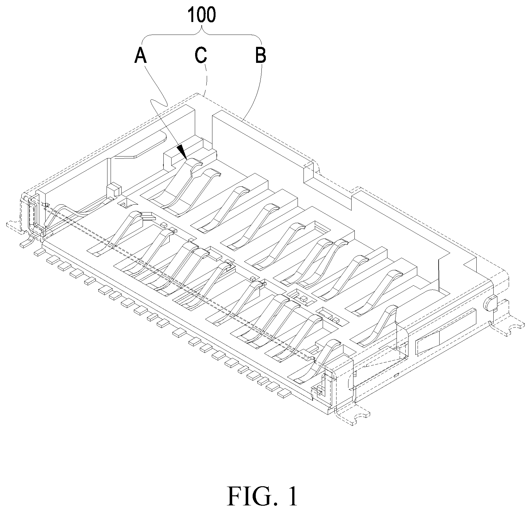
Referring to , the drawings clearly show the present invention provides a card connector 100 . The card connector 100 comprises a transmission conductor assembly A, an insulative plastic body B arranged outside the transmission conductor assembly A, and a shielding case C arranged outside the insulative plastic body B. The transmission conductor assembly A comprises:
a backup transmission conductor 01 A, wherein the backup transmission conductor 01 A has two ends that are extended to respectively form a backup soldering section 011 A and a backup spring section 012 A;
a first signal transmission conductor 02 A, wherein the first signal transmission conductor 02 A has two ends that are extended to respectively form a first signal soldering section 021 A and a first signal spring section 022 A, and the first signal soldering section 021 A is located at one side of the backup soldering section 011 A;
an inspection signal transmission conductor 03 A, wherein the inspection signal transmission conductor 03 A has two ends that are extended to respectively form an inspection signal soldering section 031 A and an inspection signal spring section 032 A, and the inspection signal soldering section 031 A is located at one side of the first signal soldering section 021 A that is distant from the backup soldering section 011 A, and the inspection signal spring section 032 A is located at one side of the first signal spring section 022 A;
a first grounding transmission conductor 04 A, wherein the first grounding transmission conductor 04 A has two ends that are extended to respectively form a first grounding soldering section 041 A and a first grounding spring section 042 A, and the first grounding soldering section 041 A is located at one side of the inspection signal soldering section 031 A that is distant from the first signal soldering section 021 A, and the first grounding spring section 042 A is located at one side of the backup spring section 012 A;
a command reset transmission conductor 05 A, wherein the command reset transmission conductor 05 A has two ends that are extended to respectively form a command reset soldering section 051 A and a command reset spring section 052 A, and the command reset soldering section 051 A is located at one side of the first grounding soldering section 041 A that is distant from the inspection signal soldering section 031 A, and the command reset spring section 052 A is located at one side of the inspection signal spring section 032 A that is distant from the first signal spring section 022 A;
a first differential transmission conductor 06 A, wherein the first differential transmission conductor 06 A has two ends that are extended to respectively form a first differential soldering section 061 A and a first differential spring section 062 A, and the first differential soldering section 061 A is located at one side of the command reset soldering section 051 A that is distant from the first grounding soldering section 041 A, and the first differential spring section 062 A is located at one side of the first grounding spring section 042 A;
a second differential transmission conductor 07 A, wherein the second differential transmission conductor 07 A has two ends that are extended to respectively form a second differential soldering section 071 A and a second differential spring section 072 A, and the second differential soldering section 071 A is located at one side of the first differential soldering section 061 A that is distant from the command reset soldering section 051 A, and the second differential spring section 072 A is located at one side of the first differential spring section 062 A that is distant from the first grounding spring section 042 A;
a second grounding transmission conductor 08 A, wherein the second grounding transmission conductor 08 A has two ends that are extended to respectively form a second grounding soldering section 081 A and a second grounding spring section 082 A, and the second grounding soldering section 081 A is located at one side of the second differential soldering section 071 A that is distant from the first differential soldering section 061 A, and the second grounding spring section 082 A is located at one side of the command reset spring section 052 A that is distant from the inspection signal spring section 032 A;
a third grounding transmission conductor 09 A, wherein the third grounding transmission conductor 09 A has two ends that are extended to respectively form a third grounding soldering section 091 A and a third grounding spring section 092 A, and the third grounding soldering section 091 A is located at one side of the second grounding soldering section 081 A that is distant from the second differential soldering section 071 A, and the third grounding spring section 092 A is located at one side of the second differential spring section 072 A that is distant from the first differential spring section 062 A;
a fourth grounding transmission conductor 10 A, wherein the fourth grounding transmission conductor 10 A has two ends that are extended to respectively form a fourth grounding soldering section 101 A and a fourth grounding spring section 102 A, and the fourth grounding soldering section 101 A is located at one side of the third grounding soldering section 091 A that is distant from the second grounding soldering section 081 A, and the fourth grounding spring section 102 A is located at one side of the second grounding spring section 082 A that is distant from the command reset spring section 052 A;
a first power transmission conductor 11 A, wherein the first power transmission conductor 11 A has two ends that are extended to respectively form a first power soldering section 111 A and a first power spring section 112 A, and the first power soldering section 111 A is located at one side of the fourth grounding soldering section 101 A that is distant from the third grounding soldering section 091 A, and the first power spring section 112 A is located at one side of the third grounding spring section 092 A that is distant from the second differential spring section 072 A;
a second power transmission conductor 12 A, wherein the second power transmission conductor 12 A has two ends that are extended to respectively form a second power soldering section 121 A and a second power spring section 122 A, and the second power soldering section 121 A is located at one side of the first power soldering section 111 A that is distant from the fourth grounding soldering section 101 A, and the second power spring section 122 A is located at one side of the fourth grounding spring section 102 A that is distant from the second grounding spring section 082 A;
a third differential transmission conductor 13 A, wherein the third differential transmission conductor 13 A has two ends that are extended to respectively form a third differential soldering section 131 A and a third differential spring section 132 A, and the third differential soldering section 131 A is located at one side of the second power soldering section 121 A that is distant from the first power soldering section 111 A, and the third differential spring section 132 A is located at one side of the first power spring section 112 A that is distant from the third grounding spring section 092 A;
a fourth differential transmission conductor 14 A, wherein the fourth differential transmission conductor 14 A has two ends that are extended to respectively form a fourth differential soldering section 141 A and a fourth differential spring section 142 A, and the fourth differential soldering section 141 A is located at one side of the third differential soldering section 131 A that is distant from the second power soldering section 121 A, and the fourth differential spring section 142 A is located at one side of the third differential spring section 132 A that is distant from the first power spring section 112 A;
a second signal transmission conductor 15 A, wherein the second signal transmission conductor 15 A has two ends that are extended to respectively form a second signal soldering section 151 A and a second signal spring section 152 A, and the second signal soldering section 151 A is located at one side of the fourth differential soldering section 141 A that is distant from the third differential soldering section 131 A, and the second signal spring section 152 A is located at one side of the second power spring section 122 A that is distant from the fourth grounding spring section 102 A;
a fifth grounding transmission conductor 16 A, wherein the fifth grounding transmission conductor 16 A has two ends that are extended to respectively form a fifth grounding soldering section 161 A and a fifth grounding spring section 162 A, and the fifth grounding soldering section 161 A is located at one side of the second signal soldering section 151 A that is distant from the fourth differential soldering section 141 A, the fifth grounding spring section 162 A is located at one side of the fourth differential spring section 142 A that is distant from the third differential spring section 132 A;
a sixth grounding transmission conductor 17 A, wherein the sixth grounding transmission conductor 17 A has two ends that are extended to respectively form a sixth grounding soldering section 171 A and a sixth grounding spring section 172 A, and the sixth grounding soldering section 171 A is located at one side of the fifth grounding soldering section 161 A that is distant from the second signal soldering section 151 A, and the sixth grounding spring section 172 A is located at one side of the second signal spring section 152 A that is distant from the second power spring section 122 A;
a seventh grounding transmission conductor 18 A, wherein the seventh grounding transmission conductor 18 A has two ends that are extended to respectively form a seventh grounding soldering section 181 A and a seventh grounding spring section 182 A, and the seventh grounding soldering section 181 A is located at one side of the sixth grounding soldering section 171 A that is distant from the fifth grounding soldering section 161 A, and the seventh grounding spring section 182 A is located at one side of the fifth grounding spring section 162 A that is distant from the fourth differential spring section 142 A;
a fifth differential transmission conductor 19 A, wherein the fifth differential transmission conductor 19 A has two ends that are extended to respectively form a fifth differential soldering section 191 A and a fifth differential spring section 192 A, and the fifth differential soldering section 191 A is located at one side of the seventh grounding soldering section 181 A that is distant from the sixth grounding soldering section 171 A, and the fifth differential spring section 192 A is located at one side of the sixth grounding spring section 172 A that is distant from the second signal spring section 152 A;
a sixth differential transmission conductor 20 A, wherein the sixth differential transmission conductor 20 A has two ends that are extended to respectively form a sixth differential soldering section 201 A and a sixth differential spring section 202 A, and the sixth differential soldering section 201 A is located at one side of the fifth differential soldering section 191 A that is distant from the seventh grounding soldering section 181 A, and the sixth differential spring section 202 A is located at one side of the fifth differential spring section 192 A that is distant from the sixth grounding spring section 172 A; and
a write-protection transmission conductor 21 A, wherein the write-protection transmission conductor 21 A has two ends that are extended to respectively form a write-protection grounding soldering section 211 A and a write-protection spring section 212 A, and the write-protection grounding soldering section 211 A is located at one side of the sixth differential soldering section 201 A that is distant from the fifth differential soldering section 191 A, and the write-protection spring section 212 A is located at one side of the seventh grounding spring section 182 A that is distant from the fifth grounding spring section 162 A.
Further, the insulative plastic body B is provided with a first signal constraining section 01 B, an inspection signal constraining section 02 B located at one side of the first signal constraining section 01 B, a command reset constraining section 03 B located at one side of the inspection signal constraining section 02 B that is distant from the first signal constraining section 01 B, a second grounding constraining section 04 B located at one side of the command reset constraining section 03 B that is distant from the inspection signal constraining section 02 B, a second power constraining section 05 B located at one side of the second grounding constraining section 04 B that is distant from the command reset constraining section 03 B, a second signal constraining section 06 B located at one side of the second power constraining section 05 B that is distant from the second grounding constraining section 04 B, a sixth grounding constraining section 07 B located at one side of the second signal constraining section 06 B that is distant from the second power constraining section 05 B, a first differential group constraining section 08 B located at one side of the sixth grounding constraining section 07 B that is distant from the second signal constraining section 06 B, a backup constraining section 09 B located at one side of the first signal constraining section 01 B, a first grounding constraining section 10 B located at one side of the backup constraining section 09 B, a second differential group constraining section 11 B located at one side of the first grounding constraining section 10 B, a third grounding constraining section 12 B located at one side of the second differential group constraining section 11 B that is distant from the first grounding constraining section 10 B, a first power constraining section 13 B located at one side of the third grounding constraining section 12 B that is distant from the second differential group constraining section 11 B, a third differential group constraining section 14 B located at one side of the first power constraining section 13 B that is distant from the third grounding constraining section 12 B, a fifth grounding constraining section 15 B located at one side of the third differential group constraining section 14 B that is distant from the first power constraining section 13 B, and a seventh grounding constraining section 16 B located at one side of the fifth grounding constraining section 15 B that is distant from the third differential group constraining section 14 B.
Further, an outside grounding transmission conductor of the transmission conductor assembly A is formed with a plurality of constraint fixing sections 22 A; and the shielding case C is provided with a plurality of collision protection sections 2 C beside an opening 1 C thereof, and the collision protection sections 2 C are connected with the transmission conductor assembly A.
Further, the fifth differential transmission conductor, the sixth differential transmission conductor, the first differential transmission conductor, the second differential transmission conductor, the third differential transmission conductor, and the fourth differential transmission conductor have widths that are greater than widths of the first signal transmission conductor, the inspection signal transmission conductor, the command reset transmission conductor, the second grounding transmission conductor, the fourth grounding transmission conductor, the second power transmission conductor, the second signal transmission conductor, the sixth grounding transmission conductor, the first grounding transmission conductor, the third grounding transmission conductor, the first power transmission conductor, the fifth grounding transmission conductor, the seventh grounding transmission conductor, and the backup transmission conductor.
The above description provides an understanding to the structure of the present invention, and based on a combination of such a structure, advantages of bettered high frequency performance, reduced capacitive effect, and suppressed electromagnetic radiation interference may be realized. Details for explanation are provided below.
A users may insert an SC card 200 through the opening 1 C into the shielding case C, and the shielding case C may reinforce an overall structural strength by means of the collision protection sections 2 C. The SC card 200 , upon insertion into the shielding case C, may attaint an effect of constraining and fixing by means of the constraint fixing sections 22 A, and is enabled to detect whether the SC card 200 de-activates the function of write protection by means of the write-protection spring section 212 A getting into engagement with the SC card 200 ; the SC card 200 is brought into contact engagement with the transmission conductor assembly A, and for the transmission conductor assembly A, the first signal spring section 022 A is received into and constrained in the first signal constraining section 01 B; the inspection signal spring section 032 A is received into and constrained in the inspection signal constraining section 02 B; the command reset spring section 052 A is received into and constrained in the command reset constraining section 03 B; the second grounding spring section 082 A is received into and constrained in the second grounding constraining section 04 B; the second power spring section 122 A is received into and constrained in the second power constraining section 05 B; the second signal spring section 152 A is received into and constrained in the second signal constraining section 06 B; the sixth grounding spring section 172 A is received into and constrained in the sixth grounding constraining section 07 B; the fifth differential spring section 192 A and the sixth differential spring section 202 A are received into and constrained in the first differential group constraining section 08 B; the backup spring section 012 A is received into and constrained in the backup constraining section 09 B; the first grounding spring section 042 A is received into and constrained in the first grounding constraining section 10 B; the first differential spring section 062 A and the second differential spring section 072 A are received into and constrained in the second differential group constraining section 11 B; the third grounding spring section 092 A is received into and constrained in the third grounding constraining section 12 B; the first power spring section 112 A is received into and constrained in the first power constraining section 13 B; the third differential spring section 132 A and the fourth differential spring section 142 A are received into and constrained in the third differential group constraining section 14 B; the fifth grounding spring section 162 A is received into and constrained in the fifth grounding constraining section 15 B; and the seventh grounding spring section 182 A is received into and constrained in the seventh grounding constraining section 16 B.
Further, contact points of the SC card 200 are set in contact engagement with the backup spring section 012 A, the first signal spring section 022 A, the inspection signal spring section 032 A, the first grounding spring section 042 A, the command reset spring section 052 A, the first differential spring section 062 A, the second differential spring section 072 A, the second grounding spring section 082 A, the third grounding spring section 092 A, the fourth grounding spring section 102 A, the first power spring section 112 A, the second power spring section 122 A, the third differential spring section 132 A, the fourth differential spring section 142 A, the second signal spring section 152 A, the fifth grounding spring section 162 A, the sixth grounding spring section 172 A, the seventh grounding spring section 182 A, the fifth differential spring section 192 A, and the sixth differential spring section 202 A of the transmission conductor assembly A, in order to establish connection between the SC card 200 and the transmission conductor assembly A. During transmission of signals, due to the first differential soldering section 061 A and the second differential soldering section 071 A, the third differential soldering section 131 A and the fourth differential soldering section 141 A, and the fifth differential soldering section 191 A and the sixth differential soldering section 201 A being respectively arranged side by side in a pairwise form, and the first differential soldering section 061 A and the second differential soldering section 071 A being provided, on two opposite sides thereof, with the first grounding soldering section 041 A and the third grounding soldering section 091 A, the third differential soldering section 131 A and the fourth differential soldering section 141 A being provided, on two opposite sides thereof, with the fourth grounding soldering section 101 A and the fifth grounding soldering section 161 A, and the fifth differential soldering section 191 A and the sixth differential soldering section 201 A being provided, on two opposite sides thereof, with the seventh grounding soldering section 181 A and the write-protection grounding soldering section 211 A, each differential group is provided, on two opposite sides thereof, with grounding sections, such that, by means of the above-described arrangement, advantages of bettering high frequency performance, reducing capacitive effect, and suppressing electromagnetic radiation interference can be realized.
Figures (8)
Citations
This patent cites (11)
- US11437745
- US20010010983
- US20040127081
- US20050227520
- US20070249202
- US20090286416
- US20140051297
- US20180138614
- US20190272453
- US20200144749
- US20230085031