Abstract
The present invention provides a dynamic comparator including a dynamic amplifier and a latch circuit. The dynamic amplifier includes a first input pair, a current source and a gain boosting circuit. The first input pair is configured to receive an input signal to generate an amplified signal at an output terminal. The current source is coupled between the first input pair and a first reference voltage. The gain-boosting circuit is coupled between the first input pair and a second reference voltage, and is configured to receive the input signal to selectively inject current to the output terminal or sink current from the output terminal. The latch circuit is coupled to the dynamic amplifier, and is configured to receive the amplified signal to generate an output signal.
Claims (11)
1. A dynamic comparator, comprising: a dynamic amplifier, comprising: a first input pair, configured to receive an input signal to generate an amplified signal at an output terminal; a current source, coupled between the first input pair and a first reference voltage; and a gain-boosting circuit, coupled between the first input pair and a second reference voltage, configured to receive the input signal to selectively inject current to the output terminal or sink current from the output terminal; and a latch circuit, coupled to the dynamic amplifier, configured to receive the amplified signal to generate an output signal; wherein the input signal is a differential input signal, the amplified signal is a differential amplified signal generated at a first output terminal and a second output terminal, the first input pair comprises a first transistor and a second transistor, and the gain-boosting circuit comprises a third transistor and a fourth transistor; and the third transistor is coupled to the first transistor via the first output terminal, the fourth transistor is coupled to the second transistor via the second output terminal, and the differential input signal is inputted into gate electrodes of the first transistor, the second transistor, the third transistor and the fourth transistor; wherein the gain-boosting circuit further comprises a fifth transistor and a sixth transistor, the fifth transistor is coupled between the third transistor and the second reference voltage, and the sixth transistor is coupled between the fourth transistor and the second reference voltage; and the current source is controlled by a first clock signal, and the fifth transistor and the sixth transistor are controlled by a second clock signal.
9. A dynamic comparator, comprising: a dynamic amplifier, comprising: a first input pair and a second input pair, configured to receive an input signal to generate an amplified signal at an output terminal; a first current source, coupled between the first input pair and a first reference voltage; and a second current source, coupled between the second input pair and a second reference voltage; and a latch circuit, coupled to the dynamic amplifier, configured to receive the amplified signal to generate an output signal; wherein the first current source and the second current source are controlled by a first clock signal, so that the first input pair samples the input signal at a rising edge of the first clock signal, and the second input pair samples the input signal at a falling edge of the first clock signal; wherein the first input pair comprises a first N-type transistor and a second N-type transistor, the second input pair comprises a first P-type transistor and a second P-type transistor, the first N-type transistor is coupled to the first P-type transistor via a first output terminal, the second N-type transistor is coupled to the second P-type transistor via a second output terminal, and an input signal is a differential input signal inputted into gate electrodes of the first N-type transistor, the second N-type transistor, the first P-type transistor and the second P-type transistor; and the first current source is implemented by a third N-type transistor, and the second current is implemented by a third-P-type transistor; wherein the dynamic amplifier further comprises a gain-boosting circuit, the gain-boosting circuit comprises a fourth N-type transistor and a fourth P-type transistor, the fourth N-type transistor is coupled between the first input pair and the first reference voltage, and the fourth P-type transistor is coupled between the second input pair and the second reference voltage.
Show 9 dependent claims
2. The dynamic comparator of claim 1 , wherein the first transistor and the second transistors are N-type transistors, and the third transistor and the fourth transistor are P-type transistors.
3. The dynamic comparator of claim 1 , wherein the first transistor and the second transistors are P-type transistors, and the third transistor and the fourth transistor are N-type transistors.
4. The dynamic comparator of claim 1 , further comprising: a logical circuit, configured to receive the first clock signal and the output signal to generate the second clock signal.
5. The dynamic comparator of claim 4 , wherein the logical circuit is configured to generate the second clock signal to enable the fifth transistor and the sixth transistor during part of an amplification phase of the dynamic amplifier, and the logical circuit is further configured to generate the second clock signal to disable the fifth transistor and the sixth transistor when the latch circuit successfully generates the output signal.
6. The dynamic comparator of claim 4 , wherein the logical circuit is an NAND gate.
7. The dynamic comparator of claim 1 , further comprising: a logical circuit, configured to receive the first clock signal and the amplified signal to generate the second clock signal, wherein the logical circuit is configured to generate the second clock signal to enable the fifth transistor and the sixth transistor during part of an amplification phase of the dynamic amplifier, and the logical circuit is further configured to generate the second clock signal to disable the fifth transistor and the sixth transistor when the latch circuit successfully generates the output signal.
8. The dynamic comparator of claim 1 , wherein the first transistor and the second transistor provide a first transconductance to increase a gain of the dynamic amplifier during a first period, the third transistor and the fourth transistor provide a second transconductance to increase the gain of the dynamic amplifier during a second period, the first period is earlier than the second period, and the first period and the second period are partially overlapped.
10. The dynamic comparator of claim 9 , wherein the fourth N-type transistor is controlled by a second clock signal, the fourth P-type transistor is controlled by a third clock signal, and the dynamic comparator further comprises: a logical circuit, wherein the logical circuit receives the first clock signal and the output signal to generate the second clock signal and the third clock signal, or the logical circuit receives the first clock signal and the amplified signal to generate the second clock signal and the third clock signal.
11. The dynamic comparator of claim 10 , wherein the logical circuit is configured to generate the third clock signal to enable the fourth P-type transistor during part of an amplification phase of the first input pair of the dynamic amplifier, and the logical circuit is further configured to generate the third clock signal to disable the fourth P-type transistor when the latch circuit successfully generates the output signal; and the logical circuit is configured to generate the second clock signal to enable the fourth N-type transistor during part of an amplification phase of the second input pair of the dynamic amplifier, and the logical circuit is further configured to generate the second clock signal to disable the fourth N-type transistor when the latch circuit successfully generates the output signal.
Full Description
Show full text →
CROSS REFERENCE TO RELATED APPLICATIONS
This application claims the priority of U.S. Provisional Application No. 63/192,139 (filed on 2021 May 24), which is included herein by reference in its entirety.
BACKGROUND
There are many applications that need high-speed and low-noise comparators, for example, a high-speed and high-resolution successive-approximation register analog-to-digital converter (SAR ADC). For the high speed consideration, a two-stage dynamic comparator is widely used because it can operate in a low supply voltage.
The conventional two-stage dynamic comparator comprises an amplifier and a latch, wherein the amplifier is used to amplify an input signal to generate an output signal, and the latch is used to store the output signal of the amplifier. The dynamic comparator works in two phases, that is an amplification phase and a reset phase. In the amplification phase, the amplifier works like an integrator to integrate the input signal, however, a gain of the amplifier is limited due to a transconductance of an input pair of the amplifier, and the limited gain will lower the noise performance. Therefore, how to provide a dynamic comparator with higher gain is an important topic.
SUMMARY
It is therefore an objective of the present invention to provide a dynamic comparator which has higher gain for a longer period of time, to solve the above-mentioned problems.
According to one embodiment of the present invention, a dynamic comparator comprising a dynamic amplifier and a latch circuit is disclosed. The dynamic amplifier comprises a first input pair, a current source and a gain boosting circuit. The first input pair is configured to receive an input signal to generate an amplified signal at an output terminal. The current source is coupled between the first input pair and a first reference voltage. The gain-boosting circuit is coupled between the first input pair and a second reference voltage, and is configured to receive the input signal to selectively inject current to the output terminal or sink current from the output terminal. The latch circuit is coupled to the dynamic amplifier, and is configured to receive the amplified signal to generate an output signal.
According to another embodiment of the present invention, a dynamic comparator comprising a dynamic amplifier and a latch circuit is disclosed. The dynamic amplifier comprises a first input pair, a second input pair, a first current source and a second current source. The first input pair and the second input pair are configured to receive an input signal to generate an amplified signal at an output terminal. The first current source is coupled between the first input pair and a first reference voltage. The second current source is coupled between the second input pair and a second reference voltage. The latch circuit is coupled to the dynamic amplifier, and is configured to receive the amplified signal to generate an output signal. In addition, the first current source and the second current source are controlled by a first clock signal, so that the first input pair samples the input signal at a rising edge of the first clock signal, and the second input pair samples the input signal at a falling edge of the first clock signal.
These and other objectives of the present invention will no doubt become obvious to those of ordinary skill in the art after reading the following detailed description of the preferred embodiment that is illustrated in the various figures and drawings.
BRIEF DESCRIPTION OF THE DRAWINGS
is a diagram illustrating a dynamic comparator according to one embodiment of the present invention.
shows a timing diagram of the signals and characteristics of the dynamic amplifier according to one embodiment of the present invention.
is a diagram illustrating the latch circuit according to one embodiment of the preset invention.
shows a diagram illustrating a logical circuit configured to generate the clock signal Clkb and the corresponding timing diagram according to one embodiment of the present invention.
shows a diagram illustrating a logical circuit configured to generate the clock signal Clkb and the corresponding timing diagram according to another embodiment of the present invention.
is a diagram illustrating a dynamic comparator according to one embodiment of the present invention.
is a diagram illustrating a dynamic comparator according to one embodiment of the present invention.
shows a timing diagram of the signals and characteristics of the dynamic amplifier of according to one embodiment of the present invention.
shows a dynamic amplifier 900 according to one embodiment of the present invention.
shows a timing diagram of the signals and characteristics of the dynamic amplifier of according to one embodiment of the present invention.
DETAILED DESCRIPTION
Certain terms are used throughout the following description and claims to refer to particular system components. As one skilled in the art will appreciate, manufacturers may refer to a component by different names. This document does not intend to distinguish between components that differ in name but not function. In the following discussion and in the claims, the terms “including” and “comprising” are used in an open-ended fashion, and thus should be interpreted to mean “including, but not limited to . . . ”. The terms “couple” and “couples” are intended to mean either an indirect or a direct electrical connection. Thus, if a first device couples to a second device, that connection may be through a direct electrical connection, or through an indirect electrical connection via other devices and connections.
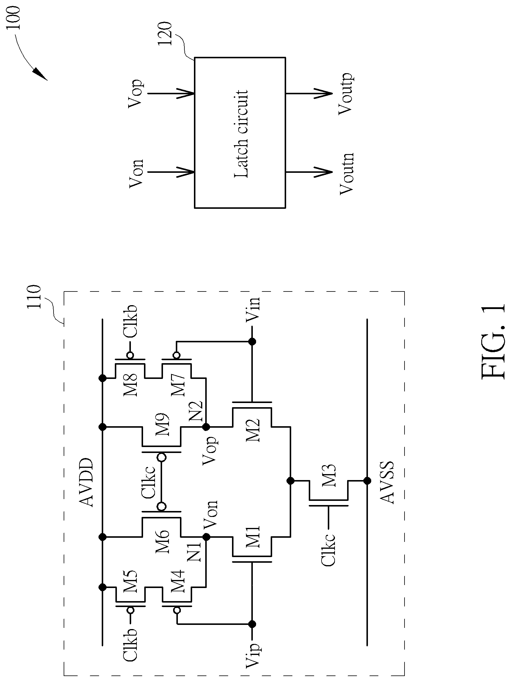
is a diagram illustrating a dynamic comparator 100 according to one embodiment of the present invention. As shown in , the dynamic comparator 100 comprises a dynamic amplifier 110 and a latch circuit 120 , wherein the dynamic amplifier 110 comprises transistors M 1 -M 9 coupled between a reference voltage AVDD (i.e. a supply voltage) and a reference voltage AVSS (i.e., aground voltage). The dynamic comparator 100 can be used in any circuit requiring higher gain and lower power consumption, such that the dynamic comparator 100 can be used in a SAR ADC.
In the dynamic comparator 100 , the dynamic amplifier 110 is configured to receive input signals Vip and Vin (differential input signal) to generate amplified signals Von and Vop (differential amplified signal) at output terminals N 1 and N 2 , and the latch circuit 120 receives the amplified signals Von and Vop to generate output signals Voutn and Voutp. Regarding the dynamic amplifier 110 , each of the transistors M 1 and M 2 is implemented by an N-type Metal-Oxide-Semiconductor (NMOS), and the transistors Ml and M 2 serve as an input pair to receive the input signals Vip and Vin to generate the amplified signals Von and Vop at the gain electrodes of the transistors M 1 and M 2 (i.e., the output terminals N 1 and N 2 ). The transistor M 3 is implemented by an NMOS coupled between the source electrode of the transistor M 1 /M 2 and the reference voltage AVSS, and the transistor M 3 serves as a current source that is used to enable or disable the amplification phase of the dynamic amplifier 110 . Each of the transistors M 4 -M 9 is implemented by a P-type Metal-Oxide-Semiconductor (PMOS), wherein the transistor M 4 is coupled to the output terminal N 1 , the transistor M 5 is coupled between the reference voltage AVDD and the transistor M 4 , the transistor M 6 is coupled between the reference voltage AVDD and the output terminal N 1 , the transistor M 7 is coupled to the output terminal N 2 , the transistor M 8 is coupled between the reference voltage AVDD and the transistor M 7 , the transistor M 9 is coupled between the reference voltage AVDD and the output terminal N 2 . The transistors M 4 and M 7 serves as another input pair to receive the differential input signal Vip and Vin to boost the gain of the dynamic amplifier 110 . In this embodiment, the transistors M 3 , M 6 and M 9 are controlled by a clock signal Clkc, and the transistors M 5 and M 8 are controlled by a clock signal Clkb, wherein the clock signal Clkc is used to enable the transistor M 3 to amplify the input signals Vip and Vin to generate the amplified signals Von and Vop, and the clock signal Clkb is used to disable the M 5 and M 8 when the latch circuit 120 successfully generates the output signals Voutn and Voutp to lower the power consumption. In addition, the clock signal Clkb is generated according to the clock signal Clkc, and the clock signal Clkb can enable or disable the transistors M 5 and M 8 at an appropriate time.
In this embodiment, the transistors M 4 , M 5 , M 7 and M 8 can be regarded as a gain-boosting circuit to boost the gain of the dynamic amplifier 110 .
Referring to and together, shows a timing diagram of the signals and characteristics of the dynamic amplifier 110 according to one embodiment of the present invention, wherein the timing diagram corresponds to a rising edge of the clock signal Clkc (i.e. the clock signal Clkc goes from a low voltage level to a high voltage level) and the following high voltage level of the clock signal Clkc. In the beginning, the clock signal Clkc has the low voltage level, so the transistor M 3 is disabled while the transistors M 6 and M 9 are enabled, and the amplified signals Von and Vop have high voltage levels. At this time, the clock signal Clkb enables the transistors M 5 and M 8 . Then, when the voltage level of the clock signal Clkc starts to increase, the transistor M 3 is enabled and a current path is formed, so that the voltage levels of the amplified signals Von and Vop starts to decrease. At this time, the dynamic amplifier 110 works like an integrator, the transistors M 1 and M 2 operate in a saturation region, and the transistors M 1 and M 2 have higher transconductance (i.e., the symbol “gmn” in ) to increase the gain of the dynamic amplifier 110 . When the amplified signals Von and Vop drop to a threshold “Vi+thp”, the transistors M 4 and M 7 start to operate in the saturation region, and the transistors M 4 and M 7 have higher transconductance (i.e., the symbol “gmp” in ) to increase the gain of the dynamic amplifier 110 , wherein “Vi” represents the input signal Vin or Vip, and “thp” represents a threshold voltage of the transistor M 4 /M 7 . Then, when the amplified signals Von and Vop drop to a threshold “Vi−thn”, the transistors M 1 and M 2 do not operate in the saturation region, and the transistors M 1 and M 2 have lower transconductance, but the transistors M 4 and M 7 still have higher transconductance to maintain the gain of the dynamic amplifier 110 . Finally, the amplified signals Von and Vop continue to decrease, and the transistors M 4 and M 7 do not operate in the saturation region so that the transistors M 4 and M 7 have lower transconductance, and the gain of the dynamic amplifier 110 decreases.
In the embodiment shown in and , the dynamic amplifier 110 has two input pairs, one input pair comprises the transistors M 1 and M 2 (NMOS), and the other input pair comprises the transistors M 4 and M 7 (PMOS). Therefore, because the transistors M 4 and M 7 are used to inject the current to the output terminals N 1 and N 2 , the gain of the dynamic amplifier 110 will increase. In addition, because the transistors M 1 and M 2 provide the tranconductance gmn during a first period, the transistors M 4 and M 7 provide the tranconductance gmp during a second period, the first period is earlier than the second period, and the second period and the first period are partially overlapped, so the dynamic amplifier 110 will have higher gain and longer amplification phase (i.e., the time the dynamic amplifier 110 has gain will become longer).
In addition, in order to ensure the normal operation of the dynamic amplifier 110 , the current provided by the PMOS M 4 /M 5 /M 7 /M 8 is smaller than the current provided by the NMOS M 1 /M 2 , so that the amplified signals Von and Vop decrease to zero during the amplification phase, to make sure that the latch circuit 120 can work properly.
is a diagram illustrating the latch circuit 120 according to one embodiment of the preset invention. As shown in , the latch circuit 120 comprises a plurality of NMOSs MN 1 -MN 8 and a plurality of PMOSs MP 1 -MP 6 coupled between the reference voltage AVDD and the reference voltage AVSS. The latch circuit 120 is used to receive the amplified signals Von and Vop to generate output signals Voutp and Voutn, and when the latch circuit 120 is ready (the output signals Voutp and Voutn are generated successfully), one of the output signals Voutp and Voutn corresponds to a high voltage level while the other one of the output signals Voutp and Voutn corresponds to a low voltage level. In addition, because a person skilled in the art should understand the operation of the latch circuit 120 , the further description of the latch circuit 120 is omitted here. It is noted that the latch circuit 120 shown in is just an example, not a limitation of the present invention.
In order to lower the power consumption, the clock signal Clkb is controlled to have the high voltage level to disable the transistors M 5 and M 8 when the latch circuit 120 is ready. shows a diagram illustrating a logical circuit 400 configured to generate the clock signal Clkb and the corresponding timing diagram according to one embodiment of the present invention. As shown in , the logical circuit 400 is implemented by a NAND gate, and the logical circuit 400 receives the clock signal Clkc, the output signals Voutn and Voutp to generate the clock signal Clkb. Specifically, when the clock signal Clkc has the high voltage level and the latch circuit 120 is not ready, all of the clock signal Clkc and the output signals Voutn/Voutp have the high voltage levels, and the clock signal Clkb has the low voltage level to enable the transistors M 5 and M 8 . Then, when the latch circuit 120 is ready (i.e., the latch goes high shown in ), one of the output signals Voutn and Voutp becomes the low voltage level, and the logical circuit 400 generates clock signal Clkb with the high voltage level to disable the transistors M 5 and M 8 .
It is noted that the NAND gate shown in is only an example, as long as the logical circuit 400 can generate the clock signal Clkb with the low voltage level to enable the transistors M 5 and M 8 during part of the amplification phase, and the logical circuit 400 can generate the clock signal Clkb with the high voltage level when the latch circuit 120 is ready, the logical circuit 400 can be implemented by other components.
shows a diagram illustrating a logical circuit 500 configured to generate the clock signal Clkb and the corresponding timing diagram according to another embodiment of the present invention. As shown in , the logical circuit 500 comprises two inverters 510 , 520 and a NAND gate 530 . The inverter 510 receives the amplified signal Vop to generate an inverted amplifier signal Vop′, the inverter 520 receives the amplified signal Von to generate an inverted amplifier signal Von′, and the NAND gate 530 receives the inverted amplifier signal Vop′, the inverted amplifier signal Von′ and the clock signal Clkc to generate the clock signal Clkb. Specifically, when the clock signal Clkc has the high voltage level and the amplified signals Vop and Von have the high voltage level (i.e., the latch circuit 120 is not ready), the clock signal Clkb has the low voltage level to enable the transistors M 5 and M 8 . Then, when the amplified signals Vop and Von have the low voltage level (i.e., the latch circuit 120 is ready), the logical circuit 400 generates clock signal Clkb with the high voltage level to disable the transistors M 5 and M 8 .
In the embodiment shown in , the inverters 510 and 520 can be replica of portion of the latch circuit 120 shown in , that is the PMOSs MP 1 , MP 2 and NMOSs MN 1 , MN 4 . Therefore, the logical circuit 400 can generate clock signal Clkb with the high voltage level disable the transistors M 5 and M 8 immediately when the latch circuit 120 is ready, to save more power consumption.
It is noted that the NAND gate shown in is only an example, as long as the logical circuit 500 can generate the clock signal Clkb based on the clock signal Clkc and the amplified signals Vop and Von, to make the clock signal Clkb has the low voltage level to enable the transistors M 5 and M 8 during part of the amplification phase, and the clock signal Clkb has the high voltage level when the latch circuit 120 is ready, the logical circuit 500 can be implemented by other components.
In the embodiment shown in , the transistors M 1 and M 2 serving as the main input pair are implemented by NMOSs, and the transistors M 4 and M 7 serving as the additional input pair are implemented by PMOSs, however in another embodiment, the main input pair can be implemented by PMOSs while the additional input pair is implemented by NMOSs. Specifically, is a diagram illustrating a dynamic comparator 600 according to one embodiment of the present invention. As shown in , the dynamic comparator 600 comprises a dynamic amplifier 610 and a latch circuit 620 , wherein the dynamic amplifier 610 comprises transistors M 1 -M 9 coupled between a reference voltage AVDD (i.e. a supply voltage) and a reference voltage AVSS (i.e., a ground voltage). The dynamic comparator 600 can be used in any circuit requiring higher gain and lower power consumption, such that the dynamic comparator 600 can be used in a SAR ADC.
In the dynamic comparator 600 , the dynamic amplifier 610 is configured to receive input signals Vip and Vin (differential input signal) to generate amplified signals Von and Vop (differential amplified signal) at output terminals N 1 and N 2 , and the latch circuit 620 receives the amplified signals Von and Vop to generate output signals Voutn and Voutp. Regarding the dynamic amplifier 610 , each of the transistors M 1 and M 2 is implemented by the PMOS, and the transistors M 1 and M 2 serve as an input pair to receive the input signals Vip and Vin to generate the amplified signals Von and Vop at the gain electrodes of the transistors M 1 and M 2 (i.e., the output terminals N 1 and N 2 ). The transistor M 3 is implemented by the PMOS coupled between the source electrode of the transistor M 1 /M 2 and the reference voltage AVDD, and the transistor M 3 serves as a current source that is used to enable or disable the amplification phase of the dynamic amplifier 610 . Each of the transistors M 4 -M 9 is implemented by the NMOS, wherein the transistors M 4 is coupled to the output terminal N 1 , the transistor M 5 is coupled between the reference voltage AVSS and the transistor M 4 , the transistor M 6 is coupled between the reference voltage AVSS and the output terminal N 1 , the transistors M 7 is coupled to the output terminal N 2 , the transistor M 8 is coupled between the reference voltage AVSS and the transistor M 7 , the transistor M 9 is coupled between the reference voltage AVSS and the output terminal N 2 . The transistors M 4 and M 7 serve as another input pair to receive the differential input signal Vip and Vin to boost the gain of the dynamic amplifier 610 . In this embodiment, the transistors M 3 , M 6 and M 9 are controlled by a clock signal Clkc, and the transistors M 5 and M 8 are controlled by a clock signal Clkb, wherein the clock signal Clkc is used to enable the transistor M 3 to amplify the input signals Vip and Vin to generate the amplified signals Von and Vop, and the clock signal Clkb is used to disable the M 5 and M 8 when the latch circuit 620 successfully generates the output signals Voutn and Voutp to lower the power consumption. In addition, the clock signal Clkb is generated according to the clock signal Clkc, and the clock signal Clkb can enable or disable the transistors M 5 and M 8 at an appropriate time.
The timing diagram of the signals in the dynamic amplifier 610 is similar to the embodiment shown in , the dynamic amplifier 610 has two input pairs, one input pair comprises the transistors M 1 and M 2 (PMOS), and the other input pair comprises the transistors M 4 and M 7 (NMOS), and because the transistors M 4 and M 7 are used to sink the current from the output terminals N 1 and N 2 , the gain of the dynamic amplifier 110 will increase. In addition, because the transistors M 1 and M 2 provide the tranconductance gmp, the transistors M 4 and M 7 provide the tranconductance gmn, and the tranconductance gmn and the tranconductance gmp are partially overlapped, so the dynamic amplifier 610 will have higher gain and longer amplification phase. In addition, the generation of the clock signal Clkb can refer to the embodiments shown in and , so the detailed descriptions of the dynamic comparator 600 are omitted here.
In the embodiments shown in , the dynamic amplifier 110 / 610 samples the input signals Vin/Vip only at the rising edge of the clock signal Clkc. In another embodiment, the dynamic amplifier can be designed to sample the input signals Vin/Vip at both the rising edge and the falling edge of the clock signal. Specifically, is a diagram illustrating a dynamic comparator 700 according to one embodiment of the present invention. As shown in , the dynamic comparator 700 comprises a dynamic amplifier 710 and two latch circuits 720 and 730 , wherein the dynamic amplifier 710 comprises transistors M 11 -M 16 coupled between a reference voltage AVDD (i.e. a supply voltage) and a reference voltage AVSS (i.e., a ground voltage). The dynamic comparator 700 can be used in any circuit requiring higher gain and lower power consumption, such that the dynamic comparator 700 can be used in a SAR ADC.
In the dynamic comparator 700 , the dynamic amplifier 710 is configured to receive input signals Vip and Vin (differential input signal) to generate amplified signals Von and Vop (differential amplified signal) at the rising edge and falling edge of the clock signal Clk, the latch circuit 720 receives the amplified signals Von and Vop generated in response to the rising edge of the clock signal Clk to generate output signals Voutn and Voutp, and the latch circuit 730 receives the amplified signals Von and Vop generated in response to the falling edge of the clock signal Clk to generate output signals Voutn and Voutp. Regarding the dynamic amplifier 710 , each of the transistors M 11 and M 12 is implemented by the NMOS, and the transistors M 11 and M 12 serve as an input pair to receive the input signals Vip and Vin to generate the amplified signals Von and Vop at the gain electrodes of the transistors M 1 and M 2 (i.e., the output terminals N 1 and N 2 ). The transistor M 13 is implemented by an NMOS coupled between the source electrode of the transistor M 11 /M 12 and the reference voltage AVSS, and the transistor M 13 serves as a current source that is used to enable or disable the amplification phase corresponding to the transistor M 11 /M 12 of the dynamic amplifier 710 . Each of the transistors M 14 and M 15 is implemented by a PMOS, wherein the transistors M 14 and M 15 serve as another input pair to receive the input signals Vip and Vin to generate the amplified signals Von and Vop at the gain electrodes of the transistors M 14 and M 15 (i.e., the output terminals N 1 and N 2 ). The transistor M 16 is implemented by a PMOS coupled between the source electrode of the transistor M 14 /M 15 and the reference voltage AVDD, and the transistor M 16 serves as a current source that is used to enable or disable the amplification phase corresponding to the transistor M 14 /M 15 of the dynamic amplifier 710 . In this embodiment, the transistors M 13 and M 16 are controlled by a clock signal Clk.
Regarding the latch circuits 720 and 730 , when the dynamic amplifier 710 samples the input signals Vin and Vip at the rising edge of the clock signal Clk to generate the amplified signals Vop and Von, the switches corresponding to the latch circuit 720 are enabled so that the latch circuit 720 receives the amplified signals Vop and Von to generate the output signals Voutp and Voutn. In addition, when the dynamic amplifier 710 samples the input signals Vin and Vip at the falling edge of the clock signal Clk to generate the amplified signals Vop and Von, the switches corresponding to the latch circuit 730 are enabled so that the latch circuit 730 receives the amplified signals Vop and Von to generate the output signals Voutp and Voutn.
shows a timing diagram of the signals and characteristics of the dynamic amplifier 710 according to one embodiment of the present invention. In the beginning, the clock signal Clk has the low voltage level, so the transistor M 13 is disabled while the transistor M 16 is enabled, and the amplified signals Von and Vop have high voltage level. Then, when the voltage level of the clock signal Clk starts to increase, the transistor M 13 is enabled and a current path is formed, so that the voltage levels of the amplified signals Von and Vop starts to decrease. At this time, the dynamic amplifier 710 works like an integrator, the transistors M 11 and M 12 operate in a saturation region, and the transistors M 11 and M 12 have higher transconductance (i.e., the symbol “gmn” in ) to increase the gain of the dynamic amplifier 710 . Then, when the amplified signals Von and Vop drop to a threshold voltage level, the transistors M 11 and M 12 do not operate in the saturation region, the transistors M 11 and M 12 have lower transconductance, and the gain of the dynamic amplifier 710 decreases.
In addition, when the voltage level of the clock signal Clk starts to decrease (i.e., falling edge), the transistor M 16 is enabled and a current path is formed, so that the voltage levels of the amplified signals Von and Vop starts to increase. At this time, the dynamic amplifier 710 works like an integrator, the transistors M 14 and M 15 operate in a saturation region, and the transistors M 14 and M 15 have higher transconductance (i.e., the symbol “gmp” in ) to increase the gain of the dynamic amplifier 710 . Then, when the amplified signals Von and Vop reach a threshold voltage level, the transistors M 14 and M 15 do not operate in the saturation region, the transistors M 14 and M 15 have lower transconductance, and the gain of the dynamic amplifier 710 decreases.
In the embodiment shown in and , the dynamic amplifier 710 have two input pairs, one input pair is the transistors M 11 and M 12 (NMOS), and the other input pair is the transistors M 14 and M 15 (PMOS). Therefore, because the two input pairs are configured to sample the input signals Vin/Vip at the rising edge and the falling edge of the clock signal Clk, respectively, the dynamic amplifier 710 will have higher efficiency.
In one embodiment, the dynamic amplifier 710 can be modified to have the gain-boosted technique shown in . Specifically, shows a dynamic amplifier 900 according to one embodiment of the present invention. As shown in , compared with the dynamic amplifier 710 , the dynamic amplifier 900 further comprises a transistor M 17 coupled between the source electrode of the transistor M 12 and the reference voltage AVSS, and a transistor M 18 coupled between the source electrode of the transistor M 15 and the reference voltage AVDD. In this embodiment, the transistors M 17 and M 18 can be regarded as a gain-boosting circuit to boost the gain of the dynamic amplifier 710 . The transistor M 17 is controlled by a clock signal Clk_bn to provide the transconductance when the transistors M 14 and M 15 of the dynamic amplifier 900 samples the input signals Vin and Vip at the falling edge of the clock signal Clk, to boost the gain of the dynamic amplifier 900 . The transistor M 18 is controlled by a clock signal Clk_bp to provide the transconductance when the transistors M 11 and M 12 of the dynamic amplifier 900 samples the input signals Vin and Vip at the rising edge of the clock signal Clk, to boost the gain of the dynamic amplifier 900 .
shows a timing diagram of the signals and characteristics of the dynamic amplifier 910 according to one embodiment of the present invention. In the beginning, the clock signal Clk has the low voltage level, so the transistor M 13 is disabled while the transistor M 16 is enabled, and the amplified signals Von and Vop have high voltage level. Then, when the voltage level of the clock signal Clk starts to increase, the transistor M 13 is enabled and a current path is formed, so that the voltage levels of the amplified signals Von and Vop starts to decrease. At this time, the dynamic amplifier 900 works like an integrator, the transistors M 11 and M 12 operate in a saturation region, and the transistors M 11 and M 12 have higher transconductance (i.e., the symbol “gmn” in ) to increase the gain of the dynamic amplifier 710 . Then, when the amplified signals Von and Vop drop to a threshold voltage such as “Vi+thp” shown in , the transistor M 18 starts to operate in the saturation region, and the transistor M 18 has higher transconductance (i.e., the symbol “gmp” in ) to increase the gain of the dynamic amplifier 710 . Then, when the amplified signals Von and Vop drop to a lower threshold voltage level, the transistors M 11 and M 12 do not operate in the saturation region, the transistors M 11 and M 12 have lower transconductance, and the gain of the dynamic amplifier 900 decreases. Therefore, because the transistors M 11 and M 12 provide the tranconductance gmn, the transistors M 14 and M 15 provides the tranconductance gmp, and the tranconductance gmn and the tranconductance gmp are partially overlapped, so the dynamic amplifier 900 will have higher gain and longer amplification phase for the sampling operation at the rising edge of the clock signal Clk.
In addition, when the voltage level of the clock signal Clk starts to decrease (i.e., falling edge), the transistor M 16 is enabled and a current path is formed, so that the voltage levels of the amplified signals Von and Vop starts to increase. At this time, the dynamic amplifier 900 works like an integrator, the transistors M 14 and M 15 operate in a saturation region, and the transistors M 14 and M 15 have higher transconductance (i.e., the symbol “gmp” in ) to increase the gain of the dynamic amplifier 900 . Then, when the amplified signals Von and Vop increase to a threshold voltage, the transistors M 11 and M 12 starts to operate in the saturation region, and the transistors M 11 and M 12 have higher transconductance (i.e., the symbol “gmn” in ) to increase the gain of the dynamic amplifier 900 . Then, when the amplified signals Von and Vop reach a higher threshold voltage level, the transistors M 14 and M 15 do not operate in the saturation region, the transistors M 14 and M 15 have lower transconductance, and the gain of the dynamic amplifier 900 decreases. Therefore, because the transistors M 14 and M 15 provide the tranconductance gmp, the transistors M 11 and M 12 provide the tranconductance gmn, and the tranconductance gmn and the tranconductance gmp are partially overlapped, so the dynamic amplifier 900 will have higher gain and longer amplification phase for the sampling operation at the falling edge of the clock signal Clk.
In addition, the clock signal Clk_bp can be generated by using any appropriate logical circuit, as long as the logical circuit can generate the clock signal Clk_bp with the low voltage level to enable the transistor M 18 during part of the amplification phase, and the logical circuit can generate the clock signal Clk_bp with the high voltage level when the latch circuit 720 is ready. For example, the clock signal Clk_bp can be generated by using the logical circuit 400 or the logical circuit 500 , that is the logical circuit can receive the output signals Voutn, Voutp and the clock signal Clk to generate the clock signal Clk_bp, or the logical circuit can receive the amplified signals Von, Vop and the clock signal Clk to generate the clock signal Clk_bp. As long as the logical circuit can generate the clock signal Clk_bp with the low voltage level to enable the transistor M 18 during part of the amplification phase, and the logical circuit can generate the clock signal Clk_bp with the high voltage level when the latch circuit 720 is ready.
Similarly, the clock signal Clk_bn can be generated by using any appropriate logical circuit, as long as the logical circuit can generate the clock signal Clk_bn with the high voltage level to enable the transistor M 17 during part of the amplification phase, and the logical circuit can generate the clock signal Clk_bn with the low voltage level when the latch circuit 730 is ready.
Briefly summarized, in the dynamic comparator of the present invention, by using the dynamic amplifier having two input pairs, the dynamic comparator will have higher gain and longer amplification phase, to improve the noise performance. In addition, the present invention further provides a dynamic amplifier capable of sampling the input signals at both the rising edge and the falling edge of the clock signal to increase the efficiency of the dynamic comparator.
Those skilled in the art will readily observe that numerous modifications and alterations of the device and method may be made while retaining the teachings of the invention. Accordingly, the above disclosure should be construed as limited only by the metes and bounds of the appended claims.
Figures (10)
Citations
This patent cites (15)
- US6157587
- US8031188
- US8829942
- US20170063361
- US20190286178
- US20190334514
- US20210067150
- US104036812
- US108347234
- US110247661
- US110289838
- US110995214
- US111313871
- US95/02280
- USWO-2021200416