Abstract
A method for manufacturing a semiconductor device includes forming a first active fin and a second active fin on a first active region and a second active region of a substrate, respectively, forming a device isolation layer to cover sidewalls of lower portions of the first active fin and the second active fin, forming a first liner layer and a second liner layer to cover upper portions of the first active fin and the second active fin, respectively, forming a first gate electrode and a second gate electrode on the first active fin and the second active fin, respectively, and forming a first source/drain region and a second source/drain region on the first active fin and the second active fin, respectively. The first liner layer includes a different material from a material of the second liner layer.
Claims (19)
1. A method for manufacturing a semiconductor device comprising: forming a first active fin and a second active fin on a first active region and a second active region of a substrate, respectively; forming a device isolation layer to cover sidewalls of lower portions of the first active fin and the second active fin; forming a first liner layer and a second liner layer to cover upper portions of the first active fin and the second active fin, respectively; performing a thermal treatment process on the substrate to oxidize the first liner layer; forming a first gate electrode and a second gate electrode on the first active fin and the second active fin, respectively; and forming a first source/drain region and a second source/drain region on the first active fin and the second active fin, respectively, wherein the first liner layer includes a material that is different from a material of the second liner layer.
10. A method for manufacturing a semiconductor device comprising: forming a first active fin and a second active fin on a first active region and a second active region of a substrate, respectively; forming a device isolation layer to cover sidewalls of lower portions of the first active fin and the second active fin; forming a first gate electrode and a second gate electrode on the first active fin and the second active fin, respectively; forming a first source/drain region and a second source/drain region on the first active fin and the second active fin, respectively; forming a protective insulating layer on sidewalls of upper portions of the first active fin and the second active fin, and the first source/drain region and the second source/drain region; forming a first air gap between the first source/drain region and the device isolation layer; and forming a second air gap between the second source/drain region and the protective insulating layer under the second source/drain region, wherein a lowermost level of the first air gap is lower than a lowermost level of the second air gap.
15. A method for manufacturing a semiconductor device comprising: forming a first active fin and a second active fin on a first active region and a second active region of a substrate, respectively; forming a device isolation layer to cover sidewalls of lower portions of the first active fin and the second active fin; forming a first gate electrode and a second gate electrode on the first active fin and the second active fin, respectively; forming a first source/drain region and a second source/drain region on the first active fin and the second active fin, respectively; and forming a protective insulating layer on sidewalls of upper portions of the first active fin and the second active fin, and the first source/drain region and the second source/drain region, wherein a thickness of the protective insulating layer on a sidewall of an upper portion of the second active fin is greater than a thickness of the protective insulating layer on the second source/drain region, and wherein a thickness of the protective insulating layer on a sidewall of an upper portion of the first active fin is substantially the same with a thickness of the protective insulating layer on the first source/drain region.
Show 16 dependent claims
2. The method of claim 1 , further comprising forming a second air gap between the second source/drain region and the second liner layer.
3. The method of claim 1 , wherein the first liner layer includes a poly-silicon layer, and wherein the second liner layer includes a silicon nitride layer.
4. The method of claim 1 , further comprising forming an etch stop layer on the first source/drain region and the second source/drain region, wherein the etch stop layer covers the second liner layer.
5. The method of claim 4 , wherein the second liner layer under the second source/drain region covers a sidewall of an upper portion of the second active fin and a top surface of the device isolation layer.
6. The method of claim 5 , wherein the second liner layer and the etch stop layer constitute a protective insulating layer, and wherein a thickness of the protective insulating layer on the sidewall of the upper portion of the second active fin is greater than a thickness of the protective insulating layer on the second source/drain region.
7. The method of claim 1 , further comprising forming an insulating pattern between the second gate electrode and the second liner layer.
8. The method of claim 1 , wherein the upper portions of the first active fin and the second active fin vertically protrude above a top surface of the device isolation layer.
9. The method of claim 1 , further comprising forming a first air gap between the first source/drain region and the device isolation layer.
11. The method of claim 10 , wherein the upper portions of the first active fin and the second active fin vertically protrude above a top surface of the device isolation layer.
12. The method of claim 10 , wherein forming the protective insulating layer comprises: forming a first liner layer and a second liner layer to cover the upper portions of the first active fin and the second active fin, respectively; and forming an etch stop layer on the second liner layer, and the first source/drain region and the second source/drain region.
13. The method of claim 12 , wherein forming the protective insulating layer further comprises performing a thermal treatment process on the substrate to oxidize the first liner layer.
14. The method of claim 10 , wherein a thickness of the protective insulating layer on a sidewall of an upper portion of the second active fin is greater than a thickness of the protective insulating layer on the second source/drain region.
16. The method of claim 15 , wherein the upper portions of the first active fin and the second active fin vertically protrude above a top surface of the device isolation layer.
17. The method of claim 15 , wherein forming the protective insulating layer comprises: forming a first liner layer and a second liner layer to cover the upper portions of the first active fin and the second active fin, respectively; and forming an etch stop layer on the second liner layer, and the first source/drain region and the second source/drain region.
18. The method of claim 17 , wherein forming the protective insulating layer further comprises performing a thermal treatment process on the substrate to oxidize the first liner layer.
19. The method of claim 17 , wherein forming the protective insulating layer further comprises forming an insulating pattern between the second gate electrode and the second liner layer.
Full Description
Show full text →
CROSS-REFERENCE TO RELATED APPLICATION
This application is a Continuation of U.S. application Ser. No. 16/793,997, filed Feb. 18, 2020, which is a Divisional of U.S. application Ser. No. 15/907,573, filed Feb. 28, 2018 (now U.S. Pat. No. 10,580,702), which claims priority under 35 U.S.C. § 119 to Korean Patent Application No. 10-2017-0098636, filed on Aug. 3, 2017, in the Korean Intellectual Property Office, the disclosures of each of which are hereby incorporated by reference in their entireties.
BACKGROUND
Embodiments of the inventive concepts relate to semiconductor devices and, more particularly, to semiconductor devices including field effect transistors.
Semiconductor devices are widely used in the electronic industry because of their small sizes, multi-functional characteristics, and/or low manufacturing costs. Semiconductor devices may be categorized as any one of semiconductor memory devices storing logical data, semiconductor logic devices processing logical data, and hybrid semiconductor devices having both the function of the semiconductor memory devices and the function of the semiconductor logic devices. Semiconductor devices with excellent characteristics have been in increasing demand with the development of the electronic industry. For example, high-reliable, high-speed, and/or multi-functional semiconductor devices have been in increasing demand. To satisfy the demand, semiconductor devices have been highly integrated and structures of semiconductor devices have become more and more complicated.
SUMMARY
Embodiments of the inventive concepts may provide a semiconductor device including a field effect transistor with improved electrical characteristics.
In an aspect, a semiconductor device includes first active patterns and second active patterns on a substrate, a first source/drain region on the first active patterns, a second source/drain region on the second active patterns and a device isolation layer filling a first trench between adjacent ones of the first active patterns and a second trench between adjacent ones of the second active patterns. A liner layer is disposed on the device isolation layer between the adjacent ones of the second active patterns. The device isolation layer between the adjacent ones of the first active patterns has a recess therein under the first source/drain region and a bottom surface of the liner layer between the adjacent ones of the second active patterns is higher than the recess.
In an aspect, a semiconductor device includes a substrate having a first region and a second region, first active patterns on the first region, second active patterns on the second region, and a device isolation layer defining the first and second active patterns on the first and second regions. A residual spacer layer is disposed on the device isolation layer between adjacent ones of the first active patterns. A liner layer is disposed on the device isolation layer between adjacent ones of the second active patterns. A pitch between the second active patterns is greater than a pitch between the first active patterns and a bottom surface of the residual spacer layer is higher than a bottom surface of the liner layer.
In an aspect, a semiconductor device includes an active fin on a substrate, a device isolation layer covering a sidewall of a lower portion of the active fin, a source/drain region on the active fin and a protective insulating layer covering a sidewall of an upper portion of the active fin and the source/drain region. A thickness of the protective insulating layer on the sidewall of the upper portion of the active fin is greater than a thickness of the protective insulating layer on the source/drain region.
BRIEF DESCRIPTION OF THE DRAWINGS
The inventive concepts will become more apparent in view of the attached drawings and accompanying detailed description.
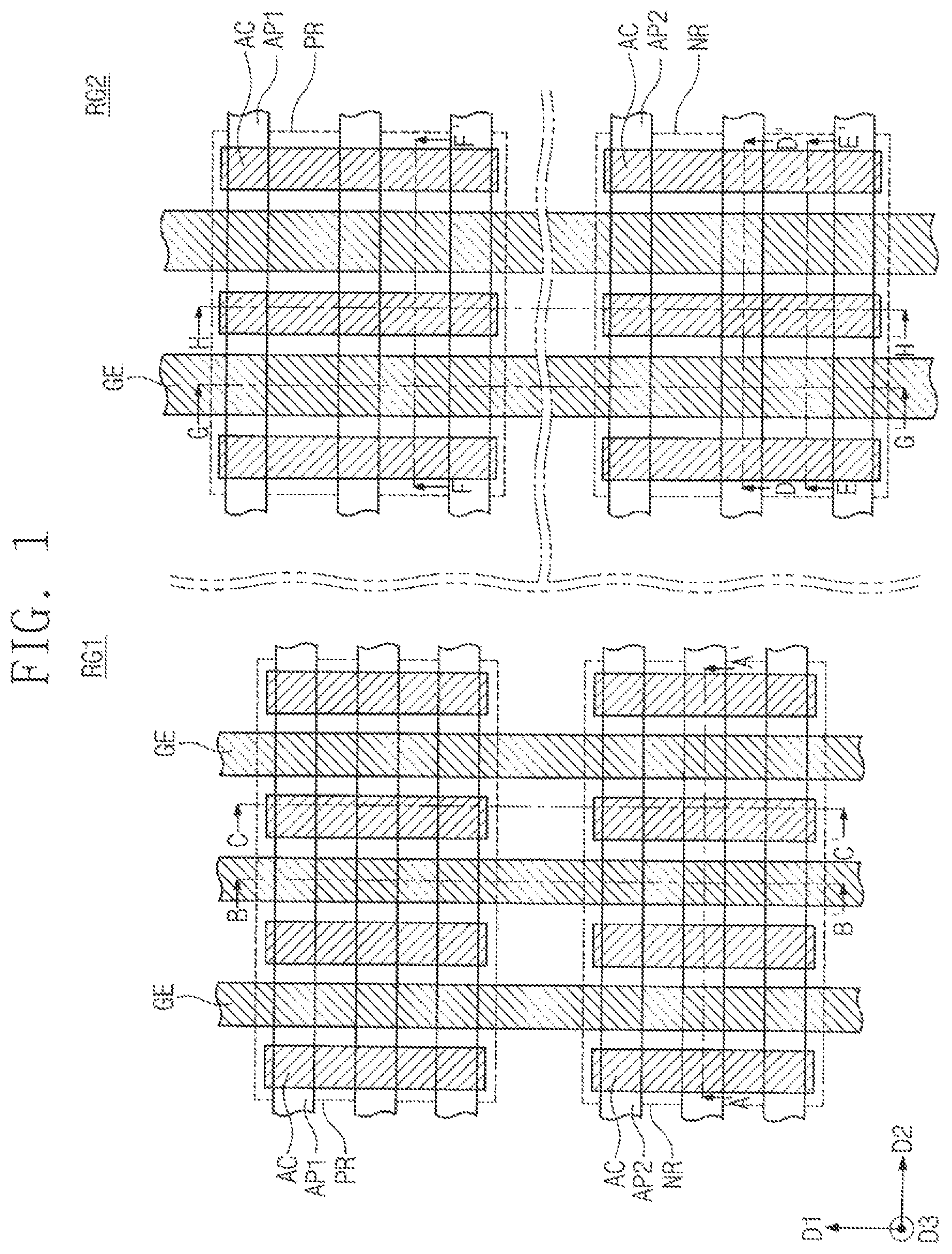
is a plan view illustrating a semiconductor device according to some embodiments of the inventive concepts.
A to 2 H are cross-sectional views taken along lines A-A′, B-B′, C-C′, D-D′, E-E′, F-F′, G-G′, and H-H′ of , respectively.
, 6 , 8 , and 10 are plan views illustrating a method for manufacturing a semiconductor device according to some embodiments of the inventive concepts.
A and 5 A are cross-sectional views taken along a line A-A′ of .
B and 5 B are cross-sectional views taken along a line B-B′ of .
C and 5 C are cross-sectional views taken along a line C-C′ of .
D and 5 D are cross-sectional views taken along a line D-D′ of .
A, 9 A, and 11 A are cross-sectional views taken along lines A-A′ of , 8 , and 10 , respectively.
B, 9 B, and 11 B are cross-sectional views taken along lines B-B′ of , 8 , and 10 , respectively.
C, 9 C, and 11 C are cross-sectional views taken along lines C-C′ of , 8 , and 10 , respectively.
D, 9 D, and 11 D are cross-sectional views taken along lines D-D′ of , 8 , and 10 , respectively.
E, 9 E, and 11 E are cross-sectional views taken along lines E-E′ of , 8 , and 10 , respectively.
F, 9 F, and 11 F are cross-sectional views taken along lines F-F′ of , 8 , and 10 , respectively.
G, 9 G, and 11 G are cross-sectional views taken along lines G-G′ of , 8 , and 10 , respectively.
H, 9 H, and 11 H are cross-sectional views taken along lines H-H′ of , 8 , and 10 , respectively.
is a cross-sectional view taken along the line C-C′ of to illustrate a semiconductor device according to some embodiments of the inventive concepts.
is a plan view illustrating a semiconductor device according to some embodiments of the inventive concepts.
A to 14 F are cross-sectional views taken along lines A-A′, B-B′, C-C′, D-D′, E-E′, and F-F′ of , respectively.
is a plan view illustrating a method for manufacturing a semiconductor device according to some embodiments of the inventive concepts.
A, 17 A, 18 A, and 19 A are cross-sectional views taken along a line A-A′ of .
B, 17 B, 18 B, and 19 B are cross-sectional views taken along a line B-B′ of .
C, 17 C, 18 C, and 19 C are cross-sectional views taken along a line C-C′ of .
D, 17 D, 18 D, and 19 D are cross-sectional views taken along a line D-D′ of .
DETAILED DESCRIPTION OF THE EMBODIMENTS
is a plan view illustrating a semiconductor device according to some embodiments of the inventive concepts. A to 2 H are cross-sectional views taken along lines A-A′, B-B′, C-C′, D-D′, E-E′, F-F′, G-G′, and H-H′ of , respectively.
A substrate 100 having a first region RG 1 and a second region RG 2 may be provided. First, the first region RG 1 of the substrate 100 will be described hereinafter in detail with reference to A to 2 C . The first region RG 1 of the substrate 100 may include a PMOSFET region PR and an NMOSFET region NR. The substrate 100 may be a semiconductor substrate including silicon, germanium, or silicon-germanium or may be a compound semiconductor substrate. For example, the substrate 100 may be a silicon substrate. The first region RG 1 may be a logic cell region on which logic transistors constituting a logic circuit of a semiconductor device are disposed. For example, logic transistors constituting a processor core may be disposed on the first region RG 1 (i.e., the logic cell region) of the substrate 100 . Some of the logic transistors may be disposed on the first region RG 1 .
A device isolation layer ST may be provided in an upper portion of the substrate 100 . The device isolation layer ST may include an insulating material such as a silicon oxide layer. The PMOSFET region PR and the NMOSFET region NR may be spaced apart from each other in a first direction D 1 with the device isolation layer ST interposed therebetween. The first direction D 1 may be parallel to a top surface of the substrate 100 . The PMOSFET region PR and the NMOSFET region NR may extend in a second direction D 2 intersecting the first direction D 1 . The device isolation layer ST between the PMOSFET region PR and the NMOSFET region NR may be deeper than the device isolation layer ST between active patterns AP 1 or AP 2 .
A plurality of the active patterns AP 1 and AP 2 extending in the second direction D 2 may be provided on the PMOSFET region PR and the NMOSFET region NR. The active patterns AP 1 and AP 2 may include first active patterns AP 1 on the PMOSFET region PR and second active patterns AP 2 on the NMOSFET region NR. The first and second active patterns AP 1 and AP 2 may be portions of the substrate 100 , which may protrude from a surface of the substrate 100 . The first and second active patterns AP 1 and AP 2 may be arranged in the first direction D 1 .
First trenches TR 1 may be defined between the first active patterns AP 1 adjacent to each other and between the second active patterns AP 2 adjacent to each other. A second trench TR 2 may be defined between the PMOSFET region PR and the NMOSFET region NR adjacent to each other. The device isolation layer ST may fill the first and second trenches TR 1 and TR 2 .
The device isolation layer ST filling the first trenches TR 1 may define the first and second active patterns AP 1 and AP 2 . The device isolation layer ST may directly cover sidewalls of lower portions of the first and second active patterns AP 1 and AP 2 . In , 2 B, and 2 C , three first active patterns AP 1 are illustrated on the PMOSFET region PR and three second active patterns AP 2 are illustrated on the NMOSFET region NR. However, embodiments of the inventive concepts are not limited thereto.
Upper portions of the first and second active patterns AP 1 and AP 2 may be higher than a top surface of the device isolation layer ST. The upper portions of the first and second active patterns AP 1 and AP 2 may vertically protrude from the device isolation layer ST. The upper portions of the first and second active patterns AP 1 and AP 2 may have fin-shapes protruding from the device isolation layer ST.
The upper portions of the first active patterns AP 1 may include first channel regions CH 1 and first source/drain regions SD 1 . The first source/drain regions SD 1 may be P-type dopant regions. Each of the first channel regions CH 1 may be disposed between a pair of the first source/drain regions SD 1 adjacent to each other. In some embodiments, three first active patterns AP 1 adjacent to each other in the first direction D 1 may share one first source/drain region SD 1 .
The upper portions of the second active patterns AP 2 may include second channel regions CH 2 and second source/drain regions SD 2 . The second source/drain regions SD 2 may be N-type dopant regions. Each of the second channel regions CH 2 may be disposed between a pair of the second source/drain regions SD 2 adjacent to each other. In some embodiments, three second active patterns AP 2 adjacent to each other in the first direction D 1 may share one second source/drain region SD 2 .
The first and second source/drain regions SD 1 and SD 2 may include epitaxial patterns formed by a selective epitaxial growth (SEG) process. Top surfaces of the first and second source/drain regions SD 1 and SD 2 may be disposed at a higher level than top surfaces of the first and second channel regions CH 1 and CH 2 . In some embodiments, the epitaxial patterns adjacent to each other in the first direction D 1 on the PMOSFET region PR may be connected to each other to constitute one first source/drain region SD 1 on the first active patterns AP 1 . The epitaxial patterns adjacent to each other in the first direction D 1 on the NMOSFET region NR may be connected to each other to constitute one second source/drain region SD 2 on the second active patterns AP 2 .
The first source/drain regions SD 1 may include a semiconductor element of which a lattice constant is greater than that of the semiconductor element of the substrate 100 . Thus, the first source/drain regions SD 1 may provide compressive stress to the first channel regions CH 1 . For example, the first source/drain regions SD 1 may include silicon-germanium (SiGe). The second source/drain regions SD 2 may include a semiconductor element of which a lattice constant is equal to or smaller than that of the semiconductor element of the substrate 100 . For example, the second source/drain regions SD 2 may include the same semiconductor element (e.g., silicon) as the substrate 100 .
Residual spacer layers RSL may be provided between the first source/drain region SD 1 and the device isolation layer ST and between the second source/drain region SD 2 and the device isolation layer ST. Each of the residual spacer layers RSL may cover the top surface of the device isolation layer ST. The residual spacer layers RSL may include the same material as gate spacers GS.
A first air gap AG 1 may be defined between the first source/drain region SD 1 and the residual spacer layer RSL. The residual spacer layer RSL may define a bottom of the first air gap AG 1 . A second air gap AG 2 may be defined between the second source/drain region SD 2 and the residual spacer layer RSL. The residual spacer layer RSL may define a bottom of the second air gap AG 2 .
Gate electrodes GE extending in the first direction D 1 may be provided on the first and second active patterns AP 1 and AP 2 to intersect the first and second active patterns AP 1 and AP 2 . The gate electrodes GE may be spaced apart from each other in the second direction D 2 . The gate electrodes GE may vertically overlap with the first and second channel regions CH 1 and CH 2 . Each of the gate electrodes GE may surround a top surface and both sidewalls of each of the first and second channel regions CH 1 and CH 2 (see B ). For example, the gate electrodes GE may include at least one of a conductive metal nitride (e.g., titanium nitride or tantalum nitride) or a metal material (e.g., titanium, tantalum, tungsten, copper, or aluminum).
A pair of gate spacers GS may be disposed on both sidewalls of each of the gate electrodes GE, respectively. The gate spacers GS may extend along the gate electrodes GE in the first direction D 1 . Top surfaces of the gate spacers GS may be higher than top surfaces of the gate electrodes GE. The top surfaces of the gate spacers GS may be coplanar with a top surface of a first interlayer insulating layer 140 to be described later. The gate spacers GS may include at least one of SiCN, SiCON, or SiN. In certain embodiments, each of the gate spacers GS may have a multi-layered structure formed of at least two of SiCN, SiCON, or SiN.
Gate dielectric patterns GI may be disposed between the gate electrodes GE and the active patterns AP 1 and AP 2 . Each of the gate dielectric patterns GI may extend along a bottom surface of each of the gate electrodes GE. Each of the gate dielectric patterns GI may cover the top surface and the both sidewalls of each of the first and second channel regions CH 1 and CH 2 . The gate dielectric patterns GI may include a high-k dielectric material. For example, the high-k dielectric material may include at least one of hafnium oxide, hafnium-silicon oxide, lanthanum oxide, zirconium oxide, zirconium-silicon oxide, tantalum oxide, titanium oxide, barium-strontium-titanium oxide, barium-titanium oxide, strontium-titanium oxide, lithium oxide, aluminum oxide, lead-scandium-tantalum oxide, or lead-zinc niobate.
A gate capping pattern GP may be provided on each of the gate electrodes GE. The gate capping patterns GP may extend along the gate electrodes GE in the first direction D 1 . The gate capping patterns GP may include a material having an etch selectivity with respect to first and second interlayer insulating layers 140 and 150 to be described later. For example, the gate capping patterns GP may include at least one of SiON, SiCN, SiCON, or SiN.
A first interlayer insulating layer 140 may be provided on the substrate 100 . The first interlayer insulating layer 140 may cover the gate spacers GS and the first and second source/drain regions SD 1 and SD 2 . A top surface of the first interlayer insulating layer 140 may be substantially coplanar with top surfaces of the gate capping patterns GP and the top surfaces of the gate spacers GS.
An etch stop layer ESL may be disposed between the first interlayer insulating layer 140 and the gate spacers GS, between the first interlayer insulating layer 140 and the source/drain regions SD 1 and SD 2 , and between the first interlayer insulating layer 140 and the device isolation layer ST. For example, the etch stop layer ESL may include a silicon nitride layer. A second interlayer insulating layer 150 may be disposed on the first interlayer insulating layer 140 and the gate capping patterns GP. For example, each of the first and second interlayer insulating layers 140 and 150 may include a silicon oxide layer.
The top surface of the device isolation layer ST between the first channel regions CH 1 and the second channel regions CH 2 spaced apart from each other in the first direction D 1 may be higher than the top surface of the device isolation layer ST between the first source/drain region SD 1 and the second source/drain region SD 2 spaced apart from each other in the first direction D 1 (see B and 2 C ). In other words, the top surface of the device isolation layer ST under the gate electrode GE may be higher than the top surface of the device isolation layer ST under the first interlayer insulating layer 140 .
At least one contact AC may penetrate the second and first interlayer insulating layers 150 and 140 between a pair of the gate electrodes GE so as to be electrically connected to the first and/or second source/drain regions SD 1 and/or SD 2 . For example, the contact AC may include at least one selected from metal materials such as aluminum, copper, tungsten, molybdenum, and cobalt.
Even though not shown in the drawings, a barrier layer may be disposed between the contact(s) AC and the source/drain regions SD 1 and SD 2 . The barrier layer may include a metal layer and/or a metal nitride layer. The metal layer may include at least one of titanium, tantalum, tungsten, nickel, cobalt, or platinum. The metal nitride layer may include at least one of a titanium nitride layer, a tantalum nitride layer, a tungsten nitride layer, a nickel nitride layer, a cobalt nitride layer, or a platinum nitride layer.
Hereinafter, the second region RG 2 of the substrate 100 will be described in detail with reference to D to 2 H . Hereinafter, the descriptions to the same technical features as mentioned with reference to A to 2 C will be omitted or mentioned briefly for the purpose of ease and convenience in explanation.
The second region RG 2 of the substrate 100 may include a PMOSFET region PR and an NMOSFET region NR. The second region RG 2 may be a peripheral circuit region of the semiconductor device. In some embodiments, the second region RG 2 may be a peripheral circuit region on which high-voltage transistors constituting an input/output (I/O) terminal are disposed.
First active patterns AP 1 may be provided on the PMOSFET region PR, and second active patterns AP 2 may be provided on the NMOSFET region NR. A distance (or a pitch), in the first direction D 1 , between the first active patterns AP 1 of the second region RG 2 may be greater than a distance (or a pitch), in the first direction D 1 , between the first active patterns AP 1 of the first region RG 1 . A distance (or a pitch), in the first direction D 1 , between the second active patterns AP 2 of the second region RG 2 may be greater than a distance (or a pitch), in the first direction D 1 , between the second active patterns AP 2 of the first region RG 1 . A width of each of the first and second active patterns AP 1 and AP 2 of the second region RG 2 may be substantially equal to a width of each of the first and second active patterns AP 1 and AP 2 of the first region RG 1 .
Upper portions of the first active patterns AP 1 may include first channel regions CH 1 and first source/drain regions SD 1 . Upper portions of the second active patterns AP 2 may include second channel regions CH 2 and second source/drain regions SD 2 . In some embodiments, the first source/drain regions SD 1 of the first active patterns AP 1 adjacent to each other in the first direction D 1 may constitute one pattern (i.e., one first source/drain region SD 1 ) in which three epitaxial patterns adjacent to each other in the first direction D 1 are merged with each other. The second source/drain regions SD 2 of the second active patterns AP 2 adjacent to each other in the first direction D 1 may constitute one pattern (i.e., one second source/drain region SD 2 ) in which three epitaxial patterns adjacent to each other in the first direction D 1 are merged with each other.
A size of the first source/drain region SD 1 of the second region RG 2 may be greater than a size of the first source/drain region SD 1 of the first region RG 1 , and a size of the second source/drain region SD 2 of the second region RG 2 may be greater than a size of the second source/drain region SD 2 of the first region RG 1 .
On the second region RG 2 , a first air gap AG 1 under the first source/drain region SD 1 may be greater than a second air gap AG 2 under the second source/drain region SD 2 . A device isolation layer ST under the first air gap AG 1 may have a recessed top surface RS. In other words, the device isolation layer ST under the first air gap AG 1 may be recessed toward a bottom surface of the substrate 100 . The recessed top surface RS of the device isolation layer ST under the first air gap AG 1 may be lower than a top surface of a device isolation layer ST under the second air gap AG 2 . In some embodiments, unlike the first region RG 1 , the residual spacer layer RSL may not exist in the first and second air gaps AG 1 and AG 2 of the second region RG 2 .
A protective insulating layer PIN may be provided on the NMOSFET region NR of the second region RG 2 . The protective insulating layer PIN may include a second liner layer LIN 2 and an etch stop layer ESL. The second liner layer LIN 2 may cover the top surface of the device isolation layer ST on the NMOSFET region NR of the second region RG 2 . The second liner layer LIN 2 may also cover sidewalls of upper portions of the second active patterns AP 2 under the second source/drain region SD 2 . The second liner layer LIN 2 may define a bottom of the second air gap AG 2 of the second region RG 2 . The second liner layer LIN 2 may not exist between the second channel regions CH 2 and the gate electrodes GE. A bottom surface of the second liner layer LIN 2 may be higher than the recessed top surface RS of the device isolation layer ST under the first air gap AG 1 .
The second liner layer LIN 2 may prevent the second active patterns AP 2 from leaning. In more detail, the second liner layer LIN 2 may reduce or minimize stress applied to the second active patterns AP 2 . For example, the second liner layer LIN 2 may include the same material (e.g., a silicon nitride layer) as the etch stop layer ESL. The silicon nitride layer may provide tensile stress to the second active patterns AP 2 , and thus electrical characteristics of an N-channel MOS field effect transistor (NMOSFET) may be improved. In addition, the silicon nitride layer may protect the second source/drain region SD 2 .
The protective insulating layer PIN may cover the sidewalls of the upper portions of the second active patterns AP 2 and the second source/drain region SD 2 . A thickness T 1 of the protective insulating layer PIN on the sidewall of the upper portion of at least one of the second active patterns AP 2 may be greater than a thickness T 2 of the protective insulating layer PIN on the second source/drain region SD 2 . This may be because the protective insulating layer PIN on the sidewall of the upper portion of at least one of the second active patterns AP 2 includes the second liner layer LIN 2 and the etch stop layer ESL but the protective insulating layer PIN on the second source/drain region SD 2 includes only the etch stop layer ESL.
A width of each of the gate electrodes GE of the second region RG 2 may be greater than a width of each of the gate electrodes GE of the first region RG 1 . The recessed top surface RS of the device isolation layer ST on the PMOSFET region PR of the second region RG 2 may be lower than a bottom surface of the gate electrode GE adjacent thereto. Insulating patterns AO may be disposed between the second liner layer LIN 2 and the gate electrodes GE on the NMOSFET region NR of the second region RG 2 . The second air gap AG 2 of the second region RG 2 may be surrounded by the gate spacers GS adjacent to each other, the insulating patterns AO adjacent to each other, the second source/drain region SD 2 , and the second liner layer LIN 2 (see E and 2 H ). For example, the insulating patterns AO may include the same material (e.g., a silicon oxide layer) as the device isolation layer ST.
, 6 , 8 , and 10 are plan views illustrating a method for manufacturing a semiconductor device according to some embodiments of the inventive concepts. A and 5 A are cross-sectional views taken along a line A-A′ of . B and 5 B are cross-sectional views taken along a line B-B′ of . C and 5 C are cross-sectional views taken along a line C-C′ of . D and 5 D are cross-sectional views taken along a line D-D′ of . A, 9 A, and 11 A are cross-sectional views taken along lines A-A′ of , 8 , and 10 , respectively. B, 9 B, and 11 B are cross-sectional views taken along lines B-B′ of , 8 , and 10 , respectively. C, 9 C, and 11 C are cross-sectional views taken along lines C-C′ of , 8 , and 10 , respectively. D, 9 D, and 11 D are cross-sectional views taken along lines D-D′ of , 8 , and 10 , respectively. E, 9 E, and 11 E are cross-sectional views taken along lines E-E′ of , 8 , and 10 , respectively. F, 9 F, and 11 F are cross-sectional views taken along lines F-F′ of , 8 , and 10 , respectively. G, 9 G, and 11 G are cross-sectional views taken along lines G-G′ of , 8 , and 10 , respectively. H, 9 H, and 11 H are cross-sectional views taken along lines H-H′ of , 8 , and 10 , respectively.
Referring to A to 4 D , a substrate 100 having a first region RG 1 and a second region RG 2 may be provided. The first region RG 1 may be a logic cell region and the second region RG 2 may be a peripheral circuit region. The substrate 100 may be patterned to form active patterns AP 1 and AP 2 . In more detail, the formation of the active patterns AP 1 and AP 2 may include forming mask patterns on the substrate 100 , and anisotropically etching the substrate 100 using the mask patterns as etch masks. First trenches TR 1 may be formed between the active patterns AP 1 and AP 2 .
A distance (i.e., a pitch), in a first direction D 1 , between the active patterns AP 1 and AP 2 on the first region RG 1 may be a first distance P 1 . A distance (i.e., a pitch), in the first direction D 1 , between the active patterns AP 1 and AP 2 on the second region RG 2 may be a second distance P 2 . The patterning process may be performed such that the second distance P 2 is greater than the first distance P 1 . In some embodiments, a width of each of the active patterns AP 1 and AP 2 on the first region RG 1 may be substantially equal to a width of each of the active patterns AP 1 and AP 2 on the second region RG 2 .
The active patterns AP 1 and AP 2 on a PMOSFET region PR and an NMOSFET region NR of the first region RG 1 may remain, but the active patterns AP 1 and AP 2 on the other region of the first region RG 1 may be removed. In more detail, a mask pattern may be formed to cover the PMOSFET region PR and the NMOSFET region NR of the first region RG 1 , and an etching process may be performed using the mask pattern as an etch mask. Thus, first active patterns AP 1 may remain on the PMOSFET region PR, and second active patterns AP 2 may remain on the NMOSFET region NR. The active patterns AP 1 and AP 2 on a PMOSFET region PR and an NMOSFET region NR of the second region RG 2 may also remain, but the active patterns AP 1 and AP 2 on the other region of the second region RG 2 may also be removed.
A second trench TR 2 deeper than the first trenches TR 1 may be formed between the PMOSFET region PR and the NMOSFET region NR of the first region RG 1 . In detail, the second trench TR 2 may be formed by etching an upper portion of the substrate 100 between the PMOSFET region PR and the NMOSFET region NR of the first region RG 1 .
A device isolation layer ST may be formed to fill the first and second trenches TR 1 and TR 2 of the first and second regions RG 1 and RG 2 of the substrate 100 . In more detail, an insulating layer (e.g., a silicon oxide layer) may be formed to completely fill the first and second trenches TR 1 and TR 2 . The insulating layer may completely cover the first and second active patterns AP 1 and AP 2 . The insulating layer may be recessed until upper portions of the first and second active patterns AP 1 and AP 2 are exposed.
The insulating layer on the first region RG 1 may be recessed (or etched) such that a top surface of the device isolation layer ST of the first region RG 1 may be disposed at a first level LV 1 . The insulating layer on the second region RG 2 may be recessed (or etched) such that a top surface of the device isolation layer ST of the second region RG 2 may be disposed at a second level LV 2 . The second level LV 2 may be lower than the first level LV 1 . Since the second distance P 2 between the active patterns AP 1 and AP 2 on the second region RG 2 is greater than the first distance P 1 between the active patterns AP 1 and AP 2 on the first region RG 1 , the insulating layer on the second region RG 2 may be etched more than the insulating layer on the first region RG 1 . In other words, an etching amount of the insulating layer on the second region RG 2 may be greater than that of the insulating layer on the first region RG 1 .
A first liner layer LIN 1 may be formed to cover the exposed upper portions of the first active patterns AP 1 on the first and second regions RG 1 and RG 2 . A second liner layer LIN 2 may be formed to cover the exposed upper portions of the second active patterns AP 2 on the first and second regions RG 1 and RG 2 . The first and second liner layers LIN 1 and LIN 2 may be formed of at least one of a silicon nitride layer, a poly-silicon layer, or a silicon oxide layer. The first and second liner layers LIN 1 and LIN 2 may include the same material or may include different materials from each other. In the present embodiment, the first liner layer LIN 1 may include the poly-silicon layer, and the second liner layer LIN 2 may include the silicon nitride layer.
The first liner layer LIN 1 and the second liner layer LIN 2 may be selectively formed on the first active patterns AP 1 and the second active patterns AP 2 , respectively. For example, the first liner layer LIN 1 may be formed on the first active patterns AP 1 by using a mask selectively opening the PMOSFET regions PR, and the second liner layer LIN 2 may be formed on the second active patterns AP 2 by using a mask selectively opening the NMOSFET regions NR.
The first and second liner layers LIN 1 and LIN 2 may prevent the first and second active patterns AP 1 and AP 2 from leaning. In more detail, the first and second liner layers LIN 1 and LIN 2 may reduce or minimize stress applied to the first and second active patterns AP 1 and AP 2 .
Referring to A to 5 D , insulating patterns AO may be formed on the first and second liner layers LIN 1 and LIN 2 of the second region RG 2 . In more detail, an additional insulating layer may be formed on an entire top surface of the substrate 100 to completely cover the first and second active patterns AP 1 and AP 2 . The additional insulating layer may be etched until upper portions of the first and second active patterns AP 1 and AP 2 are exposed. The additional insulating layer on the second region RG 2 may be etched to form the insulating patterns AO.
In some embodiments, the etching process may be performed until the first and second liner layers LIN 1 and LIN 2 on the first region RG 1 are removed. In certain embodiments, the etching process may be finished before the first and second liner layers LIN 1 and LIN 2 on the first region RG 1 are completely removed. Thus, the first and second liner layers LIN 1 and LIN 2 may also remain on the first region RG 1 even though not shown in the drawings.
Since the top surface of the device isolation layer ST on the second region RG 2 is lower than the top surface of the device isolation layer ST on the first region RG 1 , portions of the first and second liner layers LIN 1 and LIN 2 may remain on the second region RG 2 after the etching process. The insulating patterns AO on the first and second liner layers LIN 1 and LIN 2 may also remain. The first and second liner layers LIN 1 and LIN 2 remaining on the second region RG 2 may cover at least portions of sidewalls of the first and second active patterns AP 1 and AP 2 of the second region RG 2 .
Referring to A to 7 H , a thermal treatment process may be performed on the substrate 100 . Since the first liner layer LIN 1 is formed of the poly-silicon layer in the present embodiment, the first liner layer LIN 1 may be oxidized during the thermal treatment process. Thus, a silicon oxide layer may be formed from the first liner layer LIN 1 on the second region RG 2 . The oxidized first liner layer LIN 1 and the insulating patterns AO may constitute (or be included in) the device isolation layer ST (see G and 7 H ). On the contrary, the second liner layer LIN 2 on the second region RG 2 may remain after the thermal treatment process.
Sacrificial patterns PP may be formed to intersect the first and second active patterns AP 1 and AP 2 . The sacrificial patterns PP may have line shapes or bar shapes extending in the first direction D 1 . In more detail, the formation of the sacrificial patterns PP may include forming a sacrificial layer on an entire top surface of the substrate 100 , forming hard mask patterns MP on the sacrificial layer, and patterning the sacrificial layer using the hard mask patterns MP as etch masks. The sacrificial layer may include a poly-silicon layer. A width of each of the sacrificial patterns PP on the second region RG 2 may be greater than a width of each of the sacrificial patterns PP on the first region RG 1 .
A pair of gate spacers GS may be formed on both sidewalls of each of the sacrificial patterns PP, respectively. The formation of the gate spacers GS may include conformally forming a spacer layer on an entire top surface of the substrate 100 and anisotropically etching the spacer layer. For example, the spacer layer may include at least one of SiCN, SiCON, or SiN. For another example, the spacer layer may be formed of a multi-layer including at least two of SiCN, SiCON, or SiN.
The spacer layer on the active patterns AP 1 and AP 2 at both sides of each of the sacrificial patterns PP may be etched by the anisotropic etching process, and thus residual spacer layers RSL may be formed. The residual spacer layers RSL may be formed simultaneously with the gate spacers GS and may include the same material as the gate spacers GS. Since the second distance P 2 between the active patterns AP 1 and AP 2 on the second region RG 2 is greater than the first distance P 1 between the active patterns AP 1 and AP 2 on the first region RG 1 , the etching of the residual spacer layers RSL on the second region RG 2 may be more than the etching of the residual spacer layers RSL on the first region RG 1 . Thus, a thickness of the residual spacer layer RSL on the second region RG 2 may be less than a thickness of the residual spacer layer RSL on the first region RG 1 .
Referring to A to 9 H , first source/drain regions SD 1 may be formed at both sides of each of the sacrificial patterns PP on the PMOSFET regions PR, and second source/drain regions SD 2 may be formed at both sides of each of the sacrificial patterns PP on the NMOSFET regions NR.
In more detail, upper portions of the first and second active patterns AP 1 and AP 2 may be etched using the hard mask patterns MP and the gate spacers GS as etch masks to form recess regions RSG. Since the residual spacer layers RSL on the first region RG 1 are relatively thick, portions thereof may remain after the etching process. The residual spacer layers RSL on the first region RG 1 may protect the device isolation layer ST disposed thereunder during the etching process.
Since the residual spacer layers RSL on the second region GR 2 are relatively thin, the residual spacer layers RSL on the second region RG 2 may be completely removed during the etching process. Since the residual spacer layers RSL are completely removed, the device isolation layer ST on the PMOSFET region PR of the second region RG 2 may be over-etched during the etching process. Thus, the device isolation layer ST on the PMOSFET region PR of the second region RG 2 may have a recessed top surface RS. The second liner layer LIN 2 on the NMOSFET region NR of the second region RG 2 may protect the device isolation layer ST disposed thereunder during the etching process. Thus, the top surface of the device isolation layer ST on the NMOSFET region NR of the second region RG 2 may be disposed at a higher level than the recessed top surface RS of the device isolation layer ST on the PMOSFET region PR of the second region RG 2 .
First source/drain regions SD 1 may be formed by performing a selective epitaxial growth (SEG) process using inner surfaces of the recess regions RSG of the first active patterns AP 1 as seed layers. Since the first source/drain regions SD 1 are formed, a first channel region CH 1 may be defined between a pair of the first source/drain regions SD 1 . For example, the SEG process may include a chemical vapor deposition (CVD) process or a molecular beam epitaxy (MBE) process. The first source/drain regions SD 1 may include a semiconductor element of which a lattice constant is greater than that of a semiconductor element of the substrate 100 . For example, the first source/drain regions SD 1 may include silicon-germanium (SiGe).
Second source/drain regions SD 2 may be formed by performing a SEG process using inner surfaces of the recess regions RSG of the second active patterns AP 2 as seed layers. Since the second source/drain regions SD 2 are formed, a second channel region CH 2 may be defined between a pair of the second source/drain regions SD 2 . For example, the second source/drain regions SD 2 may include silicon.
The first source/drain regions SD 1 and the second source/drain regions SD 2 may be sequentially formed by different processes from each other. In other words, the first source/drain regions SD 1 may not be formed simultaneously with the second source/drain regions SD 2 .
In the present embodiment, epitaxial patterns may be merged with each other during the SEG process, and thus one first source/drain region SD 1 may be formed on the first active patterns AP 1 adjacent to each other in the first direction D 1 . Thus, a first air gap AG 1 may be formed between the first source/drain region SD 1 and the device isolation layer ST. In the present embodiment, epitaxial patterns may be merged with each other during the SEG process, and thus one second source/drain region SD 2 may be formed on the second active patterns AP 2 adjacent to each other in the first direction D 1 . Thus, a second air gap AG 2 may be formed between the second source/drain region SD 2 and the device isolation layer ST.
Referring to A to 11 H , an etch stop layer ESL may be conformally formed on an entire top surface of the substrate 100 . The etch stop layer ESL may directly cover the first and second source/drain regions SD 1 and SD 2 . The etch stop layer ESL may include a silicon nitride layer. On the NMOSFET region NR of the second region RG 2 , the etch stop layer ESL and the second liner layer LIN 2 may constitute a protective insulating layer PIN.
A first interlayer insulating layer 140 may be formed to cover the first and second source/drain regions SD 1 and SD 2 , the hard mask patterns MP, and the gate spacers GS. For example, the first interlayer insulating layer 140 may include a silicon oxide layer.
The first interlayer insulating layer 140 may be planarized until top surfaces of the sacrificial patterns PP are exposed. The planarization process of the first interlayer insulating layer 140 may be performed using an etch-back process or a chemical mechanical polishing (CMP) process. The hard mask patterns MP may be completely removed during the planarization process. As a result, a top surface of the first interlayer insulating layer 140 may be substantially coplanar with the top surfaces of the sacrificial patterns PP and top surfaces of the gate spacers GS.
The sacrificial patterns PP may be replaced with gate electrodes GE, respectively. In more detail, the exposed sacrificial patterns PP may be selectively removed. The removal of the sacrificial patterns PP may be performed using a wet etching process selectively etching silicon. During the wet etching process, an etching solution may be provided to the first source/drain region SD 1 through the first air gap AG 1 on the PMOSFET region PR of the second region RG 2 . However, since the first source/drain region SD 1 is formed of silicon-germanium (SiGe), the first source/drain region SD 1 may not be etched even though the etching solution is provided to the first source/drain region SD 1 . On the other hand, since the second source/drain region SD 2 is formed of silicon, the second source/drain region SD 2 may be etched if the etching solution is provided to the second source/drain region SD 2 . However, according to some embodiments of the inventive concepts, the second liner layer LIN 2 may remain under the sacrificial patterns PP to prevent the etching solution from being provided into the second air gap AG 2 of the second region RG 2 . On the first region RG 1 , the residual spacer layers RSL may exist between the sacrificial patterns PP and the second source/drain regions SD 2 to prevent the second source/drain regions SD 2 from being etched during the wet etching process.
A gate dielectric pattern GI, a gate electrode GE, and a gate capping pattern GP may be formed in each of empty spaces formed by the removal of the sacrificial patterns PP. The gate dielectric pattern GI may be conformally formed in the empty space and may not completely fill the empty space. The gate dielectric pattern GI may be formed using an atomic layer deposition (ALD) process or a chemical oxidation process. The gate dielectric pattern GI may include a high-k dielectric material. For example, the high-k dielectric material may include at least one of hafnium oxide, hafnium-silicon oxide, lanthanum oxide, zirconium oxide, zirconium-silicon oxide, tantalum oxide, titanium oxide, barium-strontium-titanium oxide, barium-titanium oxide, strontium-titanium oxide, lithium oxide, aluminum oxide, lead-scandium-tantalum oxide, or lead-zinc niobate.
A gate electrode layer may be formed to completely fill the empty space, and a planarization process may be performed on the gate electrode layer to form the gate electrode GE. For example, the gate electrode layer may include at least one of a conductive metal nitride (e.g., titanium nitride or tantalum nitride) or a metal material (e.g., titanium, tantalum, tungsten, copper, or aluminum).
Subsequently, upper portions of the gate electrodes GE may be recessed. The gate capping patterns GP may be formed on the recessed gate electrodes GE, respectively. The gate capping patterns GP may completely fill the recessed regions on the gate electrodes GE, respectively. For example, the gate capping patterns GP may include at least one of SiON, SiCN, SiCON, or SiN.
Referring again to A to 2 H , a second interlayer insulating layer 150 may be formed on the first interlayer insulating layer 140 and the gate capping patterns GP. The second interlayer insulating layer 150 may include a silicon oxide layer or a low-k oxide layer. For example, the low-k oxide layer may include a silicon oxide layer doped with carbon, e.g., SiCOH. The second interlayer insulating layer 150 may be formed by a CVD process.
Contacts AC may be formed to penetrate the second interlayer insulating layer 150 and the first interlayer insulating layer 140 . The contacts AC may be connected to the first and second source/drain regions SD 1 and SD 2 . In more detail, the formation of the contacts AC may include forming contact holes penetrating the second interlayer insulating layer 150 and the first interlayer insulating layer 140 , and forming a conductive layer filling the contact holes. For example, the conductive layer may include at least one of aluminum, copper, tungsten, molybdenum, or cobalt.
Subsequently, even though not shown in the drawings, an additional interlayer insulating layer and metal interconnection lines may be formed on the second interlayer insulating layer 150 .
is a cross-sectional view taken along the line C-C′ of to illustrate a semiconductor device according to some embodiments of the inventive concepts. In the present embodiment, the descriptions to the same technical features as in the embodiment of A to 2 H will be omitted for the purpose of ease and convenience in explanation. In other words, differences between the present embodiment and the embodiment of A to 2 H will be mainly described hereinafter.
Referring to , 2 H, and 12 , the second liner layer LIN 2 may be provided on the NMOSFET region NR of the first region RG 1 as well as the NMOSFET region NR of the second region RG 2 . The second liner layer LIN 2 of the NMOSFET region NR of the first region RG 1 may be disposed between the device isolation layer ST and the residual spacer layer RSL. The second liner layer LIN 2 and the etch stop layer ESL on the NMOSFET region NR of the first region RG 1 may constitute a protective insulating layer PIN of the first region RG 1 . A level of a bottom surface of the second liner layer LIN 2 on the NMOSFET region NR of the first region RG 1 may be higher than a level of a bottom surface of the second liner layer LIN 2 on the NMOSFET region NR of the second region RG 2 .
is a plan view illustrating a semiconductor device according to some embodiments of the inventive concepts. A to 14 F are cross-sectional views taken along lines A-A′, B-B′, C-C′, D-D′, E-E′, and F-F′ of , respectively. In the present embodiment, the descriptions to the same technical features as in the embodiment of A to 2 H will be omitted for the purpose of ease and convenience in explanation. In other words, differences between the present embodiment and the embodiment of A to 2 H will be mainly described hereinafter.
Referring to A to 14 F , a substrate 100 having a third region RG 3 and a fourth region RG 4 may be provided. The third region RG 3 and the fourth region RG 4 may be a logic cell region on which logic transistors for constituting a logic circuit are disposed, or a peripheral circuit region on which high-voltage transistors for constituting an I/O terminal are disposed.
A plurality of active patterns AP extending in a second direction D 2 may be provided on the third region RG 3 and the fourth region RG 4 . Widths of the active patterns AP on the third region RG 3 may be substantially equal to widths of the active patterns AP on the fourth region RG 4 . A distance (or a pitch) between the active patterns AP adjacent to each other on the third region RG 3 may be substantially equal to a distance (or a pitch) between the active patterns AP adjacent to each other on the fourth region RG 4 .
A first trench TR 1 may be defined between the active patterns AP adjacent to each other on the third region RG 3 . A second trench TR 2 may be defined between the active patterns AP adjacent to each other on the fourth region RG 4 . The second trench TR 2 may be deeper than the first trench TR 1 . In other words, heights (i.e., vertical lengths) of the active patterns AP on the third region RG 3 may be smaller than those of the active patterns AP on the fourth region RG 4 .
Each of the active patterns AP on the fourth region RG 4 may include a first portion PA 1 and a second portion PA 2 on the first portion PA 1 . The first portion PA 1 may correspond to a lower portion of the active pattern AP, and the second portion PA 2 may correspond to an upper portion of the active pattern AP. A width of the active pattern AP in a first direction D 1 may decrease as a distance from a bottom surface of the substrate 100 increases. The width of the active pattern AP may sharply (discontinuously) decrease at a boundary between the first portion PA 1 and the second portion PA 2 . In other words, a sidewall of the active pattern AP may have a stepped profile at the boundary between the first portion PA 1 and the second portion PA 2 .
Liner layers LIN may be provided on both sidewalls of the second portion PA 2 of the active pattern AP on the fourth region RG 4 . An outer sidewall of the liner layer LIN may be aligned with a sidewall of the first portion PA 1 of the active pattern AP. For example, the liner layer LIN may include at least one of a silicon nitride layer, a silicon oxide layer, or a poly-silicon layer. In certain embodiments, the liner layer LIN may have a multi-layered structure formed of at least two of the silicon nitride layer, the silicon oxide layer, or the poly-silicon layer. On the other hand, a liner layer may not exist on the third region RG 3 .
In the present embodiment, all of transistors on the third region RG 3 and the fourth region RG 4 may be P-channel MOS field effect transistors (PMOSFETs) or N-channel MOS field effect transistors (NMOSFETs). Alternatively, a conductivity type of the transistors of the third region RG 3 may be different from that of the transistors of the fourth region RG 4 . However, embodiments of the inventive concepts are not limited thereto.
is a plan view illustrating a method for manufacturing a semiconductor device according to some embodiments of the inventive concepts. A, 17 A, 18 A , and 19 A are cross-sectional views taken along a line A-A′ of . B, 17 B, 18 B, and 19 B are cross-sectional views taken along a line B-B′ of . C, 17 C, 18 C, and 19 C are cross-sectional views taken along a line C-C′ of . D, 17 D, 18 D, and 19 D are cross-sectional views taken along a line D-D′ of . In the present embodiment, the descriptions to the same technical features as in the embodiment of to 11 H will be omitted for the purpose of ease and convenience in explanation. In other words, differences between the present embodiment and the embodiment of to 11 H will be mainly described hereinafter.
Referring to A to 16 D , a substrate 100 having a third region RG 3 and a fourth region RG 4 may be provided. The third region RG 3 and the fourth region RG 4 may be a logic cell region or a peripheral circuit region. The substrate 100 may be patterned to form active patterns AP. The formation of the active patterns AP may include forming mask patterns MA on the substrate 100 , and anisotropically etching the substrate 100 using the mask patterns MA as etch masks. First trenches TR 1 may be formed between the active patterns AP.
Referring to A to 17 D , a mold layer MO may be formed on the third region RG 3 . The mold layer MO may completely cover the active patterns AP on the third region RG 3 . The mold layer MO may expose the fourth region RG 4 .
Liner layers LIN may be formed to cover exposed sidewalls of the active patterns AP on the fourth region RG 4 . In more detail, a liner layer LIN may be conformally formed on the substrate 100 , and the conformal liner layer LIN may be anisotropically etched. Thus, the liner layers LIN having spacer shapes may be formed on the sidewalls of the active patterns AP of the fourth region RG 4 . On the other hand, the third region RG 3 may be protected by the mold layer MO, and thus the liner layers LIN may not be formed on the active patterns AP of the third region RG 3 .
Referring to A to 18 D , the substrate 100 may be etched using the mold layer MO, the mask patterns MA and the liner layers LIN as etch masks to form second trenches TR 2 in the substrate 100 of the fourth region RG 4 . Due to the mold layer MO, the substrate 100 of the third region RG 3 may not be etched during the etching process. The second trenches TR 2 of the fourth region RG 4 may be deeper than the first trenches TR 1 of the third region RG 3 . Meanwhile, each of the active patterns AP on the fourth region RG 4 may include a first portion PA 1 and a second portion PA 2 on the first portion PA 1 .
Since the liner layers LIN are used as the etch masks in the etching process, a sidewall of the first portion PA 1 of the active pattern AP of the fourth region RG 4 may be aligned with an outer sidewall of the liner layer LIN. A sidewall of the active pattern AP of the fourth region RG 4 may have a stepped profile at a boundary between the first portion PA 1 and the second portion PA 2 .
Referring to A to 19 D , the mold layer MO may be removed. A device isolation layer ST may be formed in the first and second trenches TR 1 and TR 2 . In more detail, an insulating layer may be formed on the substrate 100 to completely cover the active patterns AP. The insulating layer may be planarized until top surfaces of the active patterns AP are exposed. At this time, the mask patterns MA may be removed. Thereafter, the planarized insulating layer may be recessed to expose upper portions of the active patterns AP. The recessed insulating layer may correspond to the device isolation layer ST. The liner layers LIN may also be recessed when the insulating layer is recessed.
Referring again to A to 14 F , as described above with reference to to 11 H , sacrificial patterns may be formed, source/drain regions SD may be formed at both sides of each of the sacrificial patterns, and the sacrificial patterns may be replaced with gate electrodes GE.
In the semiconductor device according to some embodiments of the inventive concepts, the liner layer may be provided on a region in which a distance between the active patterns is relatively wide. The liner layer may protect the source/drain of the NMOSFET. In addition, the liner layer may prevent the active patterns from leaning and may provide the tensile stress to the channel of the NMOSFET.
While the inventive concepts have been described with reference to example embodiments, it will be apparent to those skilled in the art that various changes and modifications may be made without departing from the spirits and scopes of the inventive concepts. Therefore, it should be understood that the above embodiments are not limiting, but illustrative. Thus, the scopes of the inventive concepts are to be determined by the broadest permissible interpretation of the following claims and their equivalents, and shall not be restricted or limited by the foregoing description.
Figures (20)
Citations
This patent cites (40)
- US7074662
- US7078286
- US7535061
- US7902035
- US8748989
- US8963279
- US9159832
- US9337260
- US9343370
- US9349632
- US9419134
- US9443757
- US9553194
- US9614059
- US9627268
- US9704737
- US9728643
- US11107734
- US11239120
- US20140036297
- US20150108544
- US20160284697
- US20160322492
- US20160329329
- US20160343709
- US20160351570
- US20160379982
- US20170025313
- US20170103985
- US20170117411
- US20170125299
- US20170125541
- US20170148914
- US20170229463
- US20170256613
- US20180182845
- US106057803
- US106098772
- US106206595
- USI582998