Processing of Circuit Boards with Protective, Adhesive-less Covers on Area Array Bonding Sites
Abstract
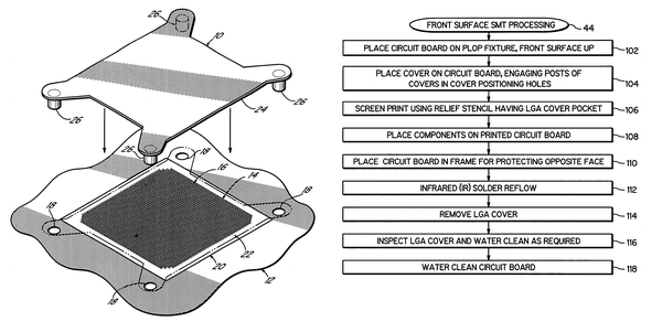
A method for processing circuit boards containing area array surface treated bonding sites, such as noble metal terminal pads of a Land Grid Array (LGA) assembly. The circuit board includes a plurality of apertures patterned about the bonding site to form a footprint. A protective cover shaped to conform to the footprint includes posts registered to removably fit into the apertures. The protective cover remains overlaid on the circuit board during fabrication processes such as solder screen printing, rework, and washing, and then removed. Thus, contamination from the fabrication processes is avoided, as well as eliminating possible sources of contamination from use of adhesive tape for protection.
Full Description
No description text available for this patent.