Abstract
A display device includes: a substrate including a first non-folding portion, a second non-folding portion, and a folding portion therebetween; a support layer disposed under the substrate and including a plurality of first portions overlapping the first and second non-folding portions, respectively, and a second portion overlapping the folding portion; a plurality of transistors disposed on the substrate, and a plurality of light emitting elements disposed above the transistors and connected to the transistors. The second portion includes a plurality of rib portions disposed between recess portions defined in a lower surface of the second portion. The folding portion includes a plurality of first folding portions overlapping the recess portions and a plurality of second folding portions overlapping the rib portions in the plan view. The transistors are not disposed in the first folding portions.
Claims (20)
1 . A display device comprising: a substrate comprising a first non-folding portion, a second non-folding portion and a folding portion therebetween; a support layer disposed under the substrate and comprising a plurality of first portions overlapping the first and second non-folding portions, respectively, and a second portion overlapping the folding portion in a plan view; a plurality of transistors disposed on the substrate; and a plurality of light emitting elements disposed above the transistors and connected to the transistors, wherein the second portion comprises a plurality of rib portions disposed between recess portions defined in a lower surface of the second portion, wherein the folding portion comprises: a plurality of first folding portions overlapping the recess portions; and a plurality of second folding portions overlapping the rib portions in the plan view, wherein the transistors are not disposed in the first folding portions.
18 . A display device comprising: a substrate comprising a first non-folding portion, a second non-folding portion, and a folding portion therebetween; a support layer disposed under the substrate and comprising a plurality of rib portions overlapping the folding portion and defining recess portions between the rib portions; a plurality of transistors disposed on the substrate; and a plurality of light emitting elements disposed above the transistors and connected to the transistors, wherein the folding portion comprises: a plurality of first folding portions overlapping the recess portions in a plan view; and a plurality of second folding portions overlapping the rib portions, wherein the transistors are disposed in the second folding portions and not disposed in the first folding portions.
Show 18 dependent claims
2 . The display device of claim 1 , wherein the rib portions extend in a first direction and are arranged spaced apart from each other in a second direction crossing the first direction, and the second non-folding portion, the folding portion, and the first non-folding portion are arranged in the second direction.
3 . The display device of claim 1 , further comprising: a buffer layer disposed on the substrate; a plurality of inorganic insulating layers disposed on the buffer layer; and at least one organic insulating layer disposed on the inorganic insulating layers, wherein the transistors are disposed on the buffer layer, some of the inorganic insulating layers are disposed on the transistors, and the light emitting elements are disposed on the at least one organic insulating layer.
4 . The display device of claim 3 , wherein at least one inorganic insulating layer among the inorganic insulating layers in an order from an uppermost layer to a lowermost layer of the inorganic insulating layers is provided with first openings defined therethrough in the first and second non-folding portions, and the first openings are defined between the light emitting elements disposed in the first and second non-folding portions in the plan view.
5 . The display device of claim 4 , wherein a material of the at least one the organic insulating layer is filled in the first openings.
6 . The display device of claim 4 , wherein at least two inorganic insulating layers among the inorganic insulating layers are provided with second openings defined therethrough in the folding portion, and the second openings are defined deeper than the first openings.
7 . The display device of claim 6 , wherein the material of the at least one the organic insulating layer is filled in the second openings.
8 . The display device of claim 6 , further comprising a plurality of light blocking layers disposed on the substrate, wherein the second openings are defined through the buffer layer.
9 . The display device of claim 6 , wherein the second openings are defined to overlap a boundary between the rib portions and the recess portions.
10 . The display device of claim 6 , wherein the transistors are disposed between the second openings in the folding portion.
11 . The display device of claim 6 , wherein the second openings are further defined between the folding portion and the first non-folding portion and between the folding portion and the second non-folding portion.
12 . The display device of claim 1 , wherein the light emitting elements are disposed in the first and second folding portions.
13 . The display device of claim 12 , wherein the transistors are disposed in the second folding portion and connected to the light emitting elements disposed in the first and second folding portions.
14 . The display device of claim 1 , wherein the transistors comprise a silicon transistor or an oxide transistor, and the oxide transistor is placed at a position higher than the silicon transistor.
15 . The display device of claim 14 , further comprising a plurality of inorganic insulating layers disposed on the substrate, wherein some of the inorganic insulating layers cover the oxide transistor and the silicon transistor.
16 . The display device of claim 1 , wherein the support layer comprises a glass material.
17 . The display device of claim 1 , wherein the recess portions extend from a same height as a lower surface of the rib portions to a point corresponding to a half of a thickness of the rib portions.
19 . The display device of claim 18 , further comprising: a buffer layer disposed on the substrate; a plurality of inorganic insulating layers disposed on the buffer layer; and at least one organic insulating layer disposed on the inorganic insulating layers, wherein at least one inorganic insulating layer among the inorganic insulating layers is provided with first openings defined therethrough in the first and second non-folding portions, at least two inorganic insulating layers among the inorganic insulating layers are provided with second openings defined therethrough in the folding portion, and the second openings are defined deeper than the first openings.
20 . The display device of claim 18 , wherein the light emitting elements are disposed in the first and second folding portions, and the transistors disposed in the second folding portions are connected to the light emitting elements disposed in the first and second folding portions.
Full Description
Show full text →
This application claims priority to Korean Patent Application No. 10-2022-0127926, filed on Oct. 6, 2022, and all the benefits accruing therefrom under 35 U.S.C. § 119, the content of which in its entirety is herein incorporated by reference.
BACKGROUND
1. Field of Disclosure
The present disclosure relates to a display device.
2. Description of the Related Art
Electronic devices that provide images to a user, such as a smart phone, a digital camera, a notebook computer, a navigation unit, and a smart television, include a display device to display the images. The display device generates the images and provides the images to the user through a display screen thereof.
With the technological development for the display device, various types of display devices are being developed. For example, various display devices, which are capable of being transformed into a curved shape, foldable, or rollable, are being developed. Those display devices are easy to carry and improve a user's convenience.
A flexible display device includes a flexible display panel. The flexible display device includes non-folding portions and a folding portion. The flexible display device is vulnerable to external impacts. In particular, the folding portion is more vulnerable to the external impacts than the non-folding portions. When transistors are damaged due to the external impacts, pixels do not function normally.
SUMMARY
The present disclosure provides a display device capable of preventing transistors from being damaged even though external impacts are applied to a folding portion thereof.
Embodiments of the invention provide a display device including: a substrate including a first non-folding portion, a second non-folding portion, and a folding portion therebetween; a support layer disposed under the substrate and including a plurality of first portions overlapping the first and second non-folding portions, respectively, and a second portion overlapping the folding portion in a plan view; a plurality of transistors disposed on the substrate; and a plurality of light emitting elements disposed above the transistors and connected to the transistors. The second portion includes a plurality of rib portions disposed between recess portions defined in a lower surface of the second portion. The folding portion includes a plurality of first folding portions overlapping the recess portions and a plurality of second folding portions overlapping the rib portions in the plan view, and the transistors are not disposed in the first folding portions.
According to the above, the support layer may be attached to a lower surface of the substrate, the transistors may be disposed on the substrate, the recess portions may be defined through the folding portion of the support layer, and the folding portion may include the rib portions disposed between the recess portions. Accordingly, the flexibility of the folding portion is effectively improved, and the support layer is folded more easily.
According to the above, the transistors may not be disposed in the first folding portions of the substrate overlapping the recess portions, but the transistors may be disposed in the second folding portions of the substrate overlapping the rib portions. Thus, the transistors are disposed more stably in the folding portion.
According to the above, first openings may be defined through inorganic layers in the first and second non-folding portions, second openings may be defined through inorganic layers in the folding portion, and the second openings may be defined deeper than the first openings. As the second openings may be defined between the first and second folding portions, the transistors may be disposed between the second openings. Therefore, when cracks occur in the inorganic layers in one folding portion due to external impacts, the cracks are not propagated to the transistors in the next folding portion and the transistors in the next folding portion are prevented from being damaged. Accordingly, the folding portion is effectively prevented from being damaged even though the external impacts are applied.
BRIEF DESCRIPTION OF THE DRAWINGS
The above and other advantages of the present disclosure will become readily apparent by reference to the following detailed description when considered in conjunction with the accompanying drawings wherein:
is a perspective view of a display device according to an embodiment of the present disclosure;
is a perspective view of a folded state of the display device shown in ;
is a cross-sectional view of the display device shown in ;
is a cross-sectional view of a display panel shown in ;
is a plan view of the display panel shown in ;
is an equivalent circuit diagram of one pixel shown in ;
is a perspective view of a support layer shown in ;
is an enlarged view of an area AA 1 shown in ;
is a cross-sectional view of a light emitting element and transistors shown in ;
is a cross-sectional view of a light emitting element and transistors disposed on a folding portion of a substrate shown in ; and
is a cross-sectional view of a display panel and a support layer according to an embodiment of the present disclosure.
DETAILED DESCRIPTION
Features of the invention and methods of accomplishing the same may be understood more readily by reference to the following detailed description of preferred embodiments and the accompanying drawings. The invention may, however, be embodied in many different forms and should not be construed as being limited to the embodiments set forth herein. Rather, these embodiments are provided so that this disclosure will be through and complete and will fully convey the invention to those skilled in the art, and the invention will only be defined by the appended claims. Like reference numerals denote like elements throughout the specification.
In the present disclosure, it will be understood that when an element or layer is referred to as being “on”, “connected to” or “coupled to” another element or layer, it can be directly on, connected or coupled to the other element or layer or intervening elements or layers may be present. The terminology used herein is for the purpose of describing particular embodiments only and is not intended to be limiting. As used herein, “a”, “an,” “the,” and “at least one” do not denote a limitation of quantity, and are intended to include both the singular and plural, unless the context clearly indicates otherwise. For example, “an element” has the same meaning as “at least one element,” unless the context clearly indicates otherwise. “At least one” is not to be construed as limiting “a” or “an.” “Or” means “and/or.” As used herein, the term “and/or” includes any and all combinations of one or more of the associated listed items.
Spatially relative terms, such as “beneath”, “below”, “lower”, “above”, “upper” and the like, may be used herein for ease of description to describe one element or feature's relationship to another element(s) or feature(s) as illustrated in the figures. It will be understood that the spatially relative terms are intended to encompass different orientations of the device in use or operation in addition to the orientation depicted in the figures
It will be understood that, although the terms “first”, “second”, etc. may be used herein to describe various elements, components, regions, layers and/or sections, these elements, components, regions, layers and/or sections should not be limited by these terms. These terms are only used to distinguish one element, component, region, layer or section from another region, layer or section. Thus, a first element, component, region, layer or section discussed below could be termed a second element, component, region, layer or section without departing from the teachings of the present disclosure.
Embodiments described in the disclosure are described with reference to plan views and cross-sectional views that are ideal schematic diagrams. Accordingly, shapes of the views may vary depending on manufacturing technologies and/or tolerances. Thus, embodiments are not limited to shown specific forms and also include variations in form produced according to manufacturing processes. Therefore, regions illustrated in the drawings are examples, and the shapes of the regions illustrated in the drawings are intended to illustrate the specific shapes of the regions of elements and not to limit the scope of the present disclosure.
It will be further understood that the terms “comprises” and/or “comprising,” or “includes” and/or “including” when used in this specification, specify the presence of stated features, regions, integers, steps, operations, elements, and/or components, but do not preclude the presence or addition of one or more other features, regions, integers, steps, operations, elements, components, and/or groups thereof. Hereinafter, embodiments of the present disclosure will be described with reference to accompanying drawings.
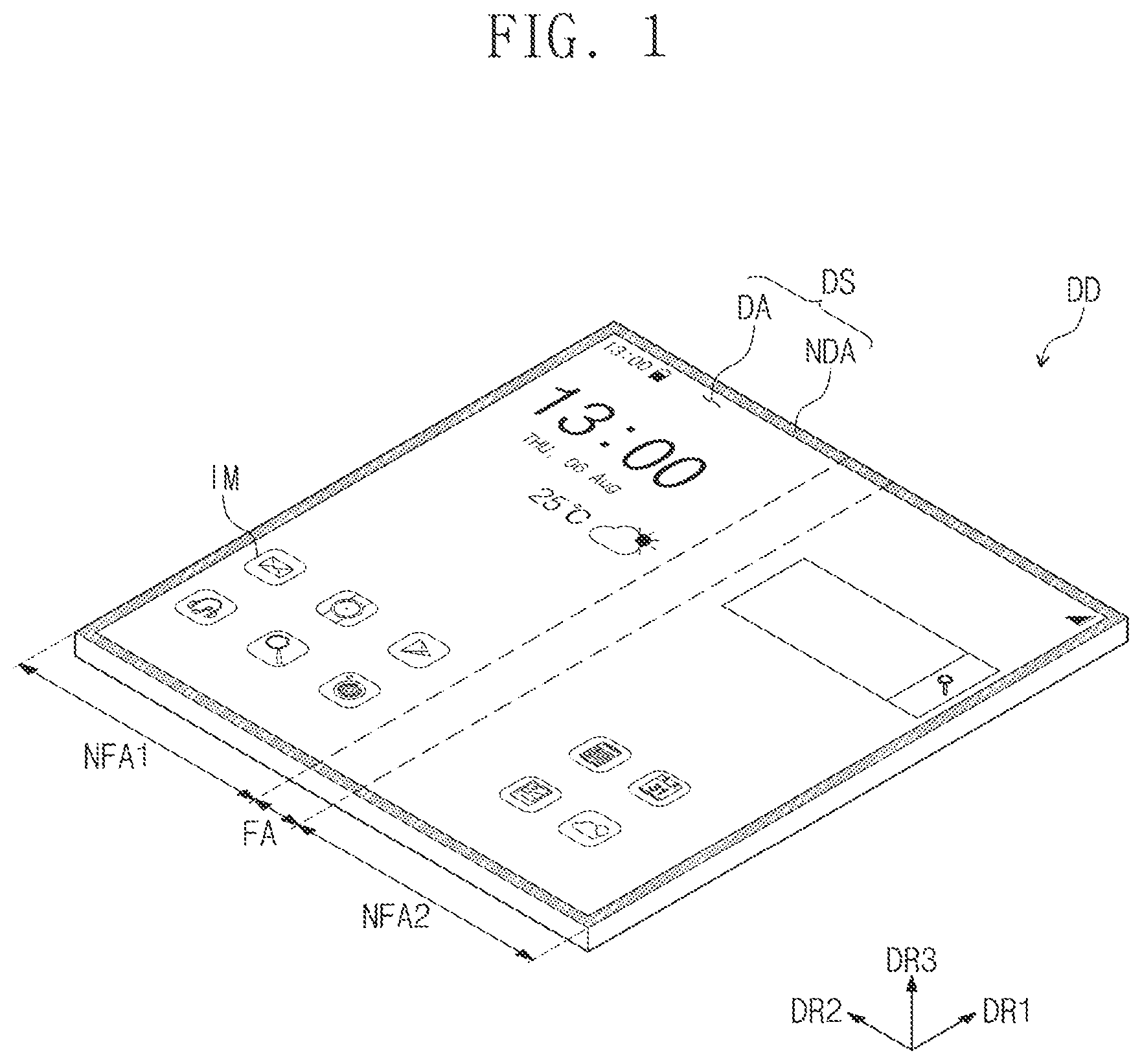
is a perspective view of a display device DD according to an embodiment of the present disclosure.
Referring to , the display device DD may have a rectangular shape defined by long sides extending in a first direction DR 1 and short sides extending in a second direction DR 2 crossing the first direction DR 1 . However, the shape of the display device DD should not be limited to the rectangular shape, and the display device DD may have various shapes, such as a circular shape and a polygonal shape. The display device DD may be a flexible display device.
The display device DD may include a folding area FA and a plurality of non-folding areas NFA 1 and NFA 2 . The non-folding areas NFA 1 and NFA 2 may include a first non-folding area NFA 1 and a second non-folding area NFA 2 . The folding area FA may be disposed between the first non-folding area NFA 1 and the second non-folding area NFA 2 . The first non-folding area NFA 1 , the folding area FA, and the second non-folding area NFA 2 may be arranged in the second direction DR 2 .
In the present embodiment, one folding area FA and two non-folding areas NFA 1 and NFA 2 are shown as a representative example, however, the number of the folding areas FA and the number of non-folding areas NFA 1 and NFA 2 should not be limited thereto or thereby. As an example, the display device DD may include more than two non-folding areas and a plurality of folding areas disposed between the non-folding areas.
An upper surface of the display device DD may be referred to as a display surface DS, and the display surface DS may be a plane defined by the first direction DR 1 and the second direction DR 2 . Images IM generated by the display device DD may be provided to a user through the display surface DS.
The display surface DS may include a display area DA and a non-display area NDA around the display area DA. The display area DA may display the image, and the non-display area NDA may not display the image. The non-display area NDA may surround the display area DA and may define an edge of the display device DD, which is printed by a predetermined color.
is a perspective view of a folded state of the display device DD shown in .
Referring to , the display device DD may be a foldable display device DD that is folded or unfolded. For example, the folding area FA may be folded with respect to a folding axis FX substantially parallel to the first direction DR 1 , and thus, the display device DD may be folded. The folding axis FX may be defined as a major axis substantially parallel to the long sides of the display device DD.
When the display device DD is folded, the display device DD may be inwardly folded (in-folding) such that the first non-folding area NFA 1 and the second non-folding area NFA 2 may face each other and the display surface DS may not be exposed to the outside. However, the present disclosure should not be limited thereto or thereby. As an example, the display device DD may be outwardly folded (out-folding) with respect to the folding axis FX such that the display surface DS may be exposed to the outside.
As shown in , a distance between the first non-folding area NFA 1 and the second non-folding area NFA 2 may be substantially the same as twice a radius of curvature R 1 .
is a cross-sectional view of the display device DD shown in .
shows a cross-section of the display device DD when viewed in the second direction DR 2 as a representative example.
The display device DD may include a display panel DP, an input sensing unit ISP, an anti-reflective layer RPL, a window WIN, a support layer GL, and first, second, and third adhesive layers AL 1 , AL 2 , and AL 3 .
The display panel DP may be a flexible display panel. The display panel DP may be a light-emitting type display panel, however, it should not be particularly limited. For instance, the display panel DP may be an organic light emitting display panel or an inorganic light emitting display panel. A light emitting layer of the organic light emitting display panel may include an organic light emitting material. A light emitting layer of the inorganic light emitting display panel may include a quantum dot or a quantum rod.
The input sensing unit ISP may be disposed on the display panel DP. The input sensing unit ISP may include a plurality of sensing portions (not shown) to sense an external input by a capacitive method. The input sensing unit ISP may be manufactured directly on the display panel DP when the display device DD is manufactured, however, it should not be limited thereto or thereby. According to an embodiment, the input sensing unit ISP may be attached to the display panel DP by an adhesive layer after being manufactured separately from the display panel DP.
The anti-reflective layer RPL may be disposed on the input sensing unit ISP. The anti-reflective layer RPL may be defined as an external light reflection preventing film. The anti-reflective layer RPL may reduce a reflectance of an external light incident to the display panel DP from the above of the display device DD.
In a case where the external light incident to the display panel DP is provided to the user after being reflected by the display panel DP, like a mirror, the user may perceive the external light. The anti-reflective layer RPL may include a plurality of color filters (not shown) that displays the same colors as pixels to prevent the above-mentioned phenomenon.
The color filters may filter the external light to allow the external light to have the same color as the pixels. In this case, the external light may not be perceived by the user, however, the present disclosure should not be limited thereto or thereby. According to an embodiment, the anti-reflective layer RPL may include a retarder and/or a polarizer to reduce the reflectance of the external light.
The window WIN may be disposed on the anti-reflective layer RPL. The window WIN may protect the display panel DP, the input sensing unit ISP, and the anti-reflective layer RPL from external scratches and impacts.
The support layer GL may be disposed under the display panel DP. The support layer GL may protect a rear surface of the display panel DP. The support layer GL may include a glass material. The support layer GL may be folded together with the display panel DP. The support layer GL will be described in detail with reference to .
The first adhesive layer AL 1 may be disposed between the display panel DP and the support layer GL. The display panel DP and the support layer GL may be coupled to each other by the first adhesive layer AL 1 . The second adhesive layer AL 2 may be disposed between the anti-reflective layer RPL and the input sensing unit ISP. The anti-reflective layer RPL and the input sensing unit ISP may be coupled to each other by the second adhesive layer AL 2 . The third adhesive layer AL 3 may be disposed between the window WIN and the anti-reflective layer RPL. The window WIN and the anti-reflective layer RPL may be coupled to each other by the third adhesive layer AL 3 .
Although not shown in figures, the display device DD may further include a panel protective film disposed under the support layer GL. The panel protective film may include a flexible plastic material such as polyethyleneterephthalate (“PET”). is a cross-sectional view of the display panel DP shown in .
shows a cross-section of the display panel DP when viewed in the second direction DR 2 as a representative example.
Referring to , the display panel DP may include a substrate SUB, a circuit element layer DP-CL disposed on the substrate SUB, a display element layer DP-OLED disposed on the circuit element layer DP-CL, and a thin film encapsulation layer TFE disposed on the display element layer DP-OLED.
The substrate SUB may include the display area DA and the non-display area NDA around the display area DA. The substrate SUB may include a flexible plastic material such as polyimide (“PI”). The display element layer DP-OLED may be disposed in the display area DA.
A plurality of pixels PX described with reference to may be disposed in the display area DA. Each pixel may include a transistor disposed on the circuit element layer DP-CL and a light emitting element disposed on the display element layer DP-OLED and connected to the transistor. The connection relationship between the transistor and the light emitting element will be described in detail with reference to .
The thin film encapsulation layer TFE may be disposed on the circuit element layer DP-CL to cover the display element layer DP-OLED. The thin film encapsulation layer TFE may include inorganic layers and an organic layer disposed between the inorganic layers. The inorganic layers may protect the pixels PX from moisture and oxygen, and the organic layer may protect the pixels PX from a foreign substance such as dust particles.
is a plan view of the display panel DP shown in , and a bottom view. As used herein, the “plan view” is a view in the third direction DR 3 in an unfolded state of the display device.
Referring to , the display device DD may include the display panel DP, a scan driver SDV, a data driver DDV, an emission driver EDV, and a plurality of pads PD.
The display panel DP may have a rectangular shape having long sides extending in the first direction DR 1 and short sides extending in the second direction DR 2 , however, the shape of the display panel DP should not be limited thereto or thereby. The display panel DP may include the display area DA and the non-display area NDA surrounding the display area DA.
The display panel DP may include the pixels PX, a plurality of scan lines SL 1 to SLm, a plurality of data lines DL 1 to DLn, a plurality of emission lines EL 1 to E 1 m , first and second control lines CSL 1 and CSL 2 , first and second power lines PL 1 and PL 2 , and connection lines CNL. Each of “m” and “n” is a natural number.
The pixels PX may be arranged in the display area DA. The scan driver SDV and the emission driver EDV may be disposed in the non-display area NDA adjacent to the long sides of the display panel DP, respectively. The data driver DDV may be disposed in the non-display area NDA to be adjacent to one short side of the short sides of the display panel DP. When viewed in a plane (i.e., in a plan view), the data driver DDV may be disposed to be adjacent to a lower end of the display panel DP.
The scan lines SL 1 to SLm may extend in the first direction DR 1 and may be connected to the pixels PX and the scan driver SDV. The data lines DL 1 to DLn may extend in the second direction DR 2 and may be connected to the pixels PX and the data driver DDV. The emission lines EL 1 to ELm may extend in the first direction DR 1 and may be connected to the pixels PX and the emission driver EDV.
The first power line PL 1 may extend in the second direction DR 2 and may be disposed in the non-display area NDA. The first power line PL 1 may be disposed between the display area DA and the emission driver EDV.
The connection lines CNL may extend in the first direction DR 1 and may be arranged in the second direction DR 2 . The connection lines CNL may be connected to the first power line PL 1 and the pixels PX. A first voltage may be applied to the pixels PX through the first power line PL 1 and the connection lines CNL connected to the first power line PL 1 . The connection lines CNL may be defined as portions of the first power line PL 1 receiving the first voltage.
The second power line PL 2 may be disposed in the non-display area NDA. The second power line PL 2 may extend along the long sides of the display panel DP and the other short side at which the data driver DDV is not disposed in the display panel DP. The second power line PL 2 may be disposed outside the scan driver SDV and the emission driver EDV.
Although not shown in figures, the second power line PL 2 may extend to the display area DA and may be connected to the pixels PX. A second voltage having a level lower than a voltage level of the first voltage may be applied to the pixels PX through the second power line PL 2 .
The first control line CSL 1 may be connected to the scan driver SDV and may extend toward the lower end of the display panel DP when viewed in a plane (i.e., in a plan view). The second control line CSL 2 may be connected to the emission driver EDV and may extend toward the lower end of the display panel DP when viewed in a plane. The data driver DDV may be disposed between the first control line CSL 1 and the second control line CSL 2 .
The pads PD may be disposed in the non-display area NDA adjacent to the lower end of the display panel DP. The pads PD may be disposed closer to the lower end of the display panel DP than the data driver DDV is. The data driver DDV, the first power line PL 1 , the second power line PL 2 , the first control line CSL 1 , and the second control line CSL 2 may be connected to the pads PD. The data lines DL 1 to DLn may be connected to the data driver DDV, and the data driver DDV may be connected to the pads PD corresponding to the data lines DL 1 to DLn.
Although not shown in figures, the display device DD may further include a timing controller to control an operation of the scan driver SDV, the data driver DDV, and the emission driver EDV and a voltage generator to generate the first and second voltages. The timing controller and the voltage generator may be connected to corresponding pads PD through a printed circuit board.
The scan driver SDV may generate a plurality of scan signals, and the scan signals may be applied to the pixels PX through the scan lines SL 1 to SLm. The data driver DDV may generate a plurality of data voltages, and the data voltages may be applied to the pixels PX through the data lines DL 1 to DLn. The emission driver EDV may generate a plurality of emission signals, and the emission signals may be applied to the pixels PX through the emission lines EL 1 to ELm.
The pixels PX may receive the data voltages in response to the scan signals. The pixels PX may emit a light having a luminance corresponding to the data voltages in response to the emission signals, and thus, the image may be displayed.
is an equivalent circuit diagram of one pixel PXij shown in .
shows the pixel PXij connected to an i-th scan line SLi, an i-th emission line ELi, and a j-th data line DLj as a representative example. In the present embodiment, each of “i” and “j” denotes a natural number.
Referring to , the pixel PXij may include a light emitting element OLED, a plurality of transistors T 1 to T 7 , and a capacitor CAP. The transistors T 1 to T 7 and the capacitor CAP may control a current amount of a current flowing through the light emitting element OLED. The light emitting element OLED may generate a light with a predetermined luminance according to the current amount of the current supplied thereto.
The i-th scan line SLi may include an i-th write scan line GWi, an i-th compensation scan line GCi, and an i-th initialization scan line GIi. The i-th write scan line GWi may receive an i-th write scan signal GWSi, the i-th compensation scan line GCi may receive an i-th compensation scan signal GCSi, and the i-th initialization scan line GIi may receive an i-th initialization scan signal GISi.
Each of the transistors T 1 to T 7 may include a source electrode, a drain electrode, and a gate electrode. In the following descriptions, for the convenience of explanation, one electrode of the source electrode and the drain electrode may be referred to as a first electrode, and the other electrode of the source electrode and the drain electrode may be referred to as a second electrode. In addition, the gate electrode may be referred to as a control electrode.
The transistors T 1 to T 7 may include first, second, third, fourth, fifth, sixth, and seventh transistors T 1 , T 2 , T 3 , T 4 , T 5 , T 6 , and T 7 . Each of the first, second, fifth, sixth, and seventh transistors T 1 , T 2 , T 5 , T 6 , and T 7 may be a PMOS transistor, and each of the third and fourth transistors T 3 and T 4 may be an NMOS transistor.
The first transistor T 1 may be defined as a driving transistor, and the second transistor T 2 may be defined as a switching transistor. The third transistor T 3 may be defined as a compensation transistor.
The fourth transistor T 4 and the seventh transistor T 7 may be defined as initialization transistors. The fifth transistor T 5 and the sixth transistor T 6 may be defined as emission control transistors.
The light emitting element OLED may be defined as an organic light emitting element. The light emitting element OLED may include an anode AE and a cathode CE. The anode AE may receive the first voltage ELVDD via the sixth, first, and fifth transistors T 6 , T 1 , and T 5 . The cathode CE may receive the second voltage ELVSS.
The first transistor T 1 may be connected between the anode AE of the light emitting element OLED and the first power line PL 1 receiving the first voltage ELVDD and may be switched on or off in response to a voltage of a node ND. In detail, the first transistor T 1 may be connected between the fifth transistor T 5 and the sixth transistor T 6 . The first transistor T 1 may receive the first voltage ELVDD via the fifth transistor T 5 and may be connected to the anode AE via the sixth transistor T 6 .
The first transistor T 1 may include a first electrode receiving the first voltage ELVDD via the fifth transistor T 5 , a second electrode connected to the anode AE via the sixth transistor T 6 , and a control electrode connected to the node ND.
The first electrode of the first transistor T 1 may be connected to the fifth transistor T 5 , the second electrode of the first transistor T 1 may be connected to the sixth transistor T 6 , and the control electrode of the first transistor T 1 may be connected to the node ND. The first transistor T 1 may control the current amount of the current flowing through the light emitting element OLED in response to the voltage of the node ND, which is applied to the control electrode of the first transistor T 1 .
The second transistor T 2 may be connected between the first transistor T 1 connected to the first power line PL 1 and the data line DLj and may be switched on or off in response to the write scan signal GWSi. In detail, the second transistor T 2 may be connected to the first power line PL 1 via the fifth transistor T 5 . The second transistor T 2 may be connected between the data line DLj and the first electrode of the first transistor T 1 .
The second transistor T 2 may include a first electrode connected to the data line DLj, a second electrode connected to the first electrode of the first transistor T 1 , and a control electrode connected to the i-th write scan line GWi.
The second transistor T 2 may be turned on in response to the i-th write scan signal GWSi applied thereto via the i-th write scan line GWi and may electrically connect the data line DLj to the first electrode of the first transistor T 1 . The second transistor T 2 may perform a switching operation to apply a data voltage Vd applied thereto via the data line DLj to the first electrode of the first transistor T 1 .
The third transistor T 3 may be connected between the node ND and the anode AE of the light emitting element OLED and may be switched on or off in response to the compensation scan signal GCSi. In detail, the third transistor T 3 may be connected to the anode AE via the sixth transistor T 6 . The third transistor T 3 may be connected between the second electrode of the first transistor T 1 and the node ND.
The third transistor T 3 may include a first electrode connected to the second electrode of the first transistor T 1 , a second electrode connected to the node ND, and a control electrode connected to the i-th compensation scan line GCi.
The third transistor T 3 may be turned on in response to the i-th compensation scan signal GCSi applied thereto via the i-th compensation scan line GCi and may electrically connect the second electrode of the first transistor T 1 to the control electrode of the first transistor T 1 . When the third transistor T 3 is turned on, the first transistor T 1 and the third transistor T 3 may be connected in a diode configuration.
The fourth transistor T 4 may be connected between the node ND and a first initialization line VIL 1 and may be switched on or off in response to the i-th initialization scan signal GISi. The fourth transistor T 4 may include a first electrode connected to the node ND, a second electrode connected to the first initialization line VIL 1 , and a control electrode connected to the i-th initialization scan line GIi.
The fourth transistor T 4 may be turned on in response to the i-th initialization scan signal GISi applied thereto via the i-th initialization scan line GIi and may apply a first initialization voltage Vint 1 applied thereto via the first initialization line VIL 1 to the node ND.
The fifth transistor T 5 may be connected between the first power line PL 1 and the first transistor T 1 . The fifth transistor T 5 may include a first electrode receiving the first voltage ELVDD, a second electrode connected to the first electrode of the first transistor T 1 , and a control electrode connected to the i-th emission line ELi.
The sixth transistor T 6 may be connected between the first transistor T 1 and the anode AE. The sixth transistor T 6 may include a first electrode connected to the second electrode of the first transistor T 1 , a second electrode connected to the anode AE, and a control electrode connected to the i-th emission line ELi.
The fifth transistor T 5 and the sixth transistor T 6 may be turned on in response to an i-th emission signal ESi applied thereto via the i-th emission line ELi. The first voltage ELVDD may be provided to the light emitting element OLED via the turned-on fifth transistor T 5 and the sixth transistor T 6 , and a driving current may flow through the light emitting element OLED. Accordingly, the light emitting element OLED may emit a light.
The seventh transistor T 7 may include a first electrode connected to the anode AE, a second electrode connected to a second initialization line VIL 2 , and a control electrode connected to an (i−1)th write scan line GWi−1. The (i−1)th write scan line GWi−1 may correspond to a write scan line of a previous stage of the i-th write scan line GWi.
The seventh transistor T 7 may be turned on in response to an (i−1)th write scan signal GWSi−1 applied thereto via the (i−1)th write scan line GWi−1 and may provide a second initialization voltage Vint 2 applied thereto via the second initialization line VIL 2 to the anode AE of the light emitting element OLED.
The seventh transistor T 7 may improve the ability to display deep black color of the pixel PX. In detail, when the seventh transistor T 7 is turned on, a parasitic capacitance (not shown) of the light emitting element OLED may be discharged. Accordingly, when implementing a black luminance, the light emitting element OLED does not emit the light even though a leakage current occurs from the first transistor T 1 , and thus the ability to display deep black color may be improved.
The capacitor CAP may include a first electrode receiving the first voltage ELVDD and a second electrode connected to the node ND. When the fifth transistor T 5 and the sixth transistor T 6 are turned on, a current amount of a current flowing through the first transistor T 1 may be determined by a voltage charged in the capacitor CAP.
is a perspective view of the support layer GL shown in .
Referring to , the support layer GL may have a rectangular shape having long sides extending in the first direction DR 1 and short sides extending in the second direction DR 2 , however, the shape of the support layer GL should not be limited thereto or thereby. The support layer GL may have a circular shape or a polygonal shape.
The support layer GL may include a plurality of first portions PT 1 and a second portion PT 2 . The second portion PT 2 may be disposed between the first portions PT 1 . The first portions PT 1 and the second portion PT 2 may be arranged in the second direction DR 2 .
When viewed in the plane (i.e., in a plan view), the first portions PT 1 may overlap the first non-folding area NFA 1 and the second non-folding area NFA 2 , respectively. As an example, the first portion PT 1 disposed at a left side may overlap the first non-folding area NFA 1 , and the first portion PT 1 disposed at a right side may overlap the second non-folding area NFA 2 . When viewed in the plane, the second portion PT 2 may overlap the folding area FA.
The second portion PT 2 may include a plurality of rib portions SLT. The rib portions SLT may be disposed at a lower surface of the second portion PT 2 . An upper surface of the second portion PT 2 may face the display panel DP. The lower surface of the second portion PT 2 may be opposite to the upper surface of the second portion PT 2 . The rib portions SLT may extend in the first direction DR 1 and may be spaced apart from each other in the second direction DR 2 .
Recess portions HEA may be defined in the lower surface of the second portion PT 2 . Each of the recess portions HEA may be defined between two rib portions SLT adjacent to each other.
The recess portions HEA may extend from the lower surface of the second portion PT 2 toward the upper surface of the second portion PT 2 . As an example, a depth in a third direction DR 3 of the recess portions HEA may correspond to a half of a thickness of the support layer GL. That is, the recess portions HEA may extend from the same height as the lower surface of the rib portions SLT to a point corresponding to the half of the thickness of the rib portions SLT. However, the depth in the third direction DR 3 of the recess portions HEA should not be limited thereto or thereby, and the recess portions HEA may extend to the same height as the upper surface of the rib portions SLT in another embodiment. In this case, the rib portions SLT may be separated (i.e., not connected) from each other in the second direction DR 2 . As used herein, the “thickness” is measured in the third direction DR 3 when the display device is in an unfolded state.
As the recess portions HEA are defined in the second portion PT 2 , the area of the second portion PT 2 in a cross-sectional view may be reduced, and the rigidity of the support layer GL may be reduced. Accordingly, the flexibility of the support layer GL may be higher when the recess portions HEA are defined than when the recess portions HEA are not defined in the support layer GL. As a result, the support layer GL may be folded more easily.
is an enlarged view of an area AA 1 shown in .
For convenience of description, the first to seventh transistors T 1 to T 7 shown in are schematically illustrated as one transistor TR in . Hereinafter, each of the transistors TR will be defined as including first to seventh transistors. In addition, the transistors TR disposed on the substrate SUB will be described.
Referring to , 7 , and 8 , the substrate SUB may include a folding portion FP and first and second non-folding portions NFP 1 and NFP 2 . The folding portion FP may be disposed between the first and second non-folding portions NFP 1 and NFP 2 . The first non-folding portion NFP 1 , the folding portion FP, and the second non-folding portion NFP 2 may be sequentially arranged in the second direction DR 2 . When viewed in the plane (i.e., in a plan view), the folding portion FP may overlap the folding area FA, and the first and second non-folding portions NFP 1 and NFP 2 may overlap the first and second folding areas NFA 1 and NFA 2 , respectively.
The folding portion FP of the substrate SUB may include a plurality of first folding portions FP 1 and a plurality of second folding portions FP 2 . When viewed in the plane, the first folding portions FP 1 may overlap the recess portions HEA shown in . When viewed in the plane (i.e., in a plan view), the second folding portions FP 2 may overlap the rib portions SLT shown in .
The data lines DL 1 to DLn and the pixels PX may be disposed on the substrate SUB. Each of the pixels PX may include the light emitting element OLED and the transistor TR connected to the light emitting element OLED. For the convenience of explanation, shows a structure in which one transistor TR is connected to one light emitting element OLED. However, substantially the first to seventh transistors T 1 to T 7 shown in may be connected to a corresponding light emitting element OLED among the light emitting elements OLED. The data lines DL 1 to DLn may extend from the first non-folding portion NFP 1 to the second direction DR 2 and may extend to the second non-folding portion NFP 2 after passing through the folding portion FP.
The light emitting elements OLED and the transistors TR may be disposed on the first non-folding portion NFP 1 , the second non-folding portion NFP 2 , and the folding portion FP. The light emitting elements OLED may be disposed on the first folding portions FP 1 and the second folding portions FP 2 . The transistors TR may be disposed on the second folding portions FP 2 and may not be disposed on the first folding portions FP 1 .
Since the transistors TR are not disposed on the first folding portions FP 1 , the transistors TR may not overlap the recess portion HEA when viewed in the plane (i.e., in a plan view). The transistors TR may overlap the rib portions SLT when viewed in the plane. The light emitting elements OLED may not overlap the transistors TR in the first folding portions FP 1 .
Each of the light emitting elements OLED disposed on the first folding portions FP 1 may be connected to some transistors TR among the transistors TR disposed on the second folding portions FP 2 adjacent thereto. Each of the light emitting elements OLED disposed on the second folding portions FP 2 may be connected to the other transistors TR among the transistors TR disposed on the second folding portions FP 2 . The connection relationship between the transistors TR and the light emitting elements OLED, which are disposed on the folding portion FP, will be described in detail with reference to .
is a cross-sectional view of one pixel disposed in the first non-folding portion NFP 1 in .
shows the first transistor T 1 , the fourth transistor T 4 , and the sixth transistor T 6 shown in as a representative example.
In , the second non-folding portion NFP 2 may be substantially the same as the first non-folding portion NFP 1 . Hereinafter, descriptions are made based on components of the pixel PX disposed in the first non-folding portion NFP 1 , and the structure of the pixel PX disposed in the second non-folding portion NFP 2 may be substantially the same as the structure of the pixel PX of .
Referring to , the pixel PX may include the light emitting elements OLED and the transistors T 1 , T 4 , and T 6 . Although not shown figures, the pixel PX may include second, third, fifth, and seventh transistors T 2 , T 3 , T 5 , and T 7 and at least one capacitor CAP.
A buffer layer BFL may be disposed on the substrate SUB. The buffer layer BFL may be an inorganic layer. A first semiconductor pattern SMP 1 of each of the first and sixth transistors T 1 and T 6 may be disposed on the buffer layer BFL. Each of the first and sixth transistors T 1 and T 6 may be a silicon transistor. The first semiconductor pattern SMP 1 may include polysilicon, however, the present disclosure should not be limited thereto or thereby. According to an embodiment, the first semiconductor pattern SMP 1 may include amorphous silicon.
The first semiconductor pattern SMP 1 may be doped with an N-type dopant or a P-type dopant. The first semiconductor pattern SMP 1 may include a high-doped region and a low-doped region. The high-doped region may have a conductivity greater than a conductivity of the low-doped region and may substantially serve as a source electrode and a drain electrode of the transistor TR. The low-doped region may substantially correspond to an active (or a channel) of the transistor TR.
A source electrode S 1 , an active A 1 , and a drain electrode D 1 of the first transistor T 1 and a source electrode S 6 , an active A 6 , and a drain electrode D 6 of the sixth transistor T 6 may be formed from the first semiconductor pattern SMP 1 . The active A 1 may be disposed between the source electrode S 1 and the drain electrode D 1 . The active A 6 may be disposed between the source electrode S 6 and the drain electrode D 6 .
A first insulating layer INS 1 may be disposed on the buffer layer BFL to cover the first semiconductor pattern SMP 1 . Gate electrodes G 1 and G 6 (or control electrodes) of the first and sixth transistors T 1 and T 6 may be disposed on the first insulating layer INS 1 .
Although not shown in figures, a source electrode, an active, a drain electrode, and a gate electrode of each of the second, fifth, and seventh transistors T 2 , T 5 , and T 7 may have substantially the same structure as those of the first and sixth transistors T 1 and T 6 .
A second insulating layer INS 2 may be disposed on the first insulating layer INS 1 to cover the gate electrodes G 1 and G 6 . A dummy electrode DME may be disposed on the second insulating layer INS 2 . The dummy electrode DME may be placed at a position higher than the first and sixth transistors T 1 and T 6 . The dummy electrode DME may form the above-mentioned capacitor CAP together with the gate electrode G 1 . A third insulating layer INS 3 may be disposed on the second insulating layer INS 2 to cover the dummy electrode DME.
A second semiconductor pattern SMP 2 of the fourth transistor T 4 may be disposed on the third insulating layer INS 3 . The fourth transistor T 4 may be placed at a position higher than the first and sixth transistors T 1 and T 6 . The fourth transistor T 4 may be an oxide transistor. The second semiconductor pattern SMP 2 may include an oxide semiconductor containing metal oxide. The oxide semiconductor may include a crystalline or amorphous oxide semiconductor.
The second semiconductor pattern SMP 2 may include a plurality of areas having different electrical properties depending on whether the metal oxide is reduced. An area (hereinafter, referred to as a reduced area) where the metal oxide is reduced may have a conductivity higher than a conductivity of an area (hereinafter, referred to as a non-reduced area) where the metal oxide is not reduced. The reduced area may substantially act as the source electrode or the drain electrode of the transistor. The non-reduced area may substantially correspond to the active (or channel) of the transistor.
A source electrode S 4 , an active A 4 , and a drain electrode D 4 of the fourth transistor T 4 may be formed from the second semiconductor pattern SMP 2 . The active A 4 may be disposed between the source electrode S 4 and the drain electrode D 4 .
A fourth insulating layer INS 4 may be disposed on the third insulating layer INS 3 to cover the second semiconductor pattern SMP 2 . A gate electrode G 4 (or a control electrode) of the fourth transistor T 4 may be disposed on the fourth insulating layer INS 4 . A fifth insulating layer INS 5 may be disposed on the fourth insulating layer INS 4 to cover the gate electrode G 4 . Although not shown in figures, a source electrode, an active, a drain electrode, and a gate electrode of the third transistor T 3 may have substantially the same structure as those of the fourth transistor T 4 .
The buffer layer BFL and the first to fifth insulating layers INS 1 to INS 5 may include inorganic layers. As an example, the buffer layer BFL and the first insulating layer INS 1 may include a silicon oxide layer, and the second insulating layer INS 2 may include a silicon nitride layer. The third insulating layer INS 3 may include a plurality of inorganic insulating layers containing different materials from each other and stacked one on another. As an example, the third insulating layer INS 3 may include a silicon nitride layer and a silicon oxide layer, which are stacked on each other.
The fourth insulating layer INS 4 may include a silicon oxide layer. The fifth insulating layer INS 5 may include a plurality of inorganic insulating layers containing different materials from each other and stacked one on another. As an example, the fifth insulating layer INS 5 may include a silicon oxide layer and a silicon nitride layer, which are stacked on each other. Each of the third and fifth insulating layers INS 3 and INS 5 may have a thickness greater than a thickness of each of the buffer layer BFL and the first, second, and fourth insulating layers INS 1 , INS 2 , and INS 4 . Hereinafter, the first to fifth insulating layers INS 1 to INS 5 may be referred to as the inorganic insulating layers.
A first connection electrode CNE 1 may be disposed on the fifth insulating layer INS 5 . The first connection electrode CNE 1 may be connected to the drain electrode D 6 via a first contact hole CH 1 defined through the first to fifth insulating layer INS 1 to INS 5 .
The substrate SUB may include a first boundary portion BA 1 . The first boundary portion BA 1 may be provided in plural. The first boundary portions BA 1 may correspond to an area between two light emitting elements OLED adjacent to each other among the light emitting elements OLED disposed on the first and second non-folding portions NFP 1 and NFP 2 .
First openings OP 1 may be defined in the first boundary portions BA 1 . The first openings OP 1 may overlap the first boundary portions BA 1 . When viewed in the plane (i.e., in a plan view), the first openings OP 1 may be defined between two light emitting elements OLED adjacent to each other among the light emitting elements OLED disposed in the first and second non-folding portions NFP 1 and NFP 2 . The first to seventh transistors T 1 to T 7 described with reference to may be disposed between the first openings OP 1 .
The first openings OP 1 may be defined through at least one of the inorganic insulating layers INS 1 to INS 5 in an order from the uppermost layer (i.e., INS 5 ) to the lowermost layer (i.e., INS 1 ). As an example, the first openings OP 1 may be defined through the fifth inorganic insulating layer INS 5 .
Organic insulating layers INS 6 and INS 7 may be disposed on the buffer layer BFL and the inorganic insulating layers INS 1 to INS 5 . The organic insulating layers INS 6 and INS 7 may include a sixth insulating layer INS 6 and a seventh insulating layer INS 7 . The sixth and seventh insulating layers INS 6 and INS 7 may include an organic layer.
The sixth insulating layer INS 6 may be disposed on the fifth insulating layer INS 5 to cover the first connection electrode CNE 1 . The sixth insulating layer INS 6 may be disposed in the first openings OP 1 , and the first openings OP 1 may be filled with a material of the sixth insulating layer INS 6 .
A second connection electrode CNE 2 may be disposed on the sixth insulating layer INS 6 . The second connection electrode CNE 2 may be connected to the first connection electrode CNE 1 via a second contact hole CH 2 defined through the sixth insulating layer INS 6 .
A conductive pattern CLS may be disposed on the sixth insulating layer INS 6 . The conductive pattern CLS may be the data lines DL 1 to DLn or the first power line PL 1 shown in .
The seventh insulating layer INS 7 may be disposed on the sixth insulating layer INS 6 to cover the second connection electrode CNE 2 and the conductive pattern CLS.
The light emitting element OLED may be disposed on the seventh insulating layer INS 7 . The light emitting element OLED may include a first electrode AE, a second electrode CE, a hole control layer HCL, an electron control layer ECL, and a light emitting layer EML. The first electrode AE may be the anode AE shown in , and the second electrode CE may be the cathode CE shown in .
The first electrode AE may be disposed on the seventh insulating layer INS 7 . The first electrode AE may be electrically connected to the second connection electrode CNE 2 via a third contact hole CH 3 defined through the seventh insulating layer INS 7 . A pixel definition layer PDL that exposes a predetermined portion of the first electrode AE may be disposed on the first electrode AE and the seventh insulating layer INS 7 . An opening PX_OP may be defined through the pixel definition layer PDL to expose the predetermined portion of the first electrode AE.
The hole control layer HCL may be disposed on the first electrode AE and the pixel definition layer PDL. The hole control layer HCL may be commonly disposed in a light emitting area LEA and a non-light-emitting area NLEA. The hole control layer HCL may include a hole transport layer and a hole injection layer.
The light emitting layer EML may be disposed on the hole control layer HCL. The light emitting layer EML may be disposed in an area corresponding to the opening PX_OP. The light emitting layer EML may include an organic material and/or an inorganic material. The light emitting layer EML may emit one of a red light, a green light, and a blue light.
The electron control layer ECL may be disposed on the light emitting layer EML and the hole control layer HCL. The electron control layer ECL may be commonly disposed in the light emitting area LEA and the non-light-emitting area NLEA. The electron control layer ECL may include an electron transport layer and an electron injection layer. The second electrode CE may be disposed on the electron control layer ECL. The second electrode CE may be commonly disposed over the pixels PX.
The thin film encapsulation layer TFE may be disposed on the light emitting element OLED. The thin film encapsulation layer TFE may include an inorganic layer, an organic layer, and an inorganic layer, which are sequentially stacked. The inorganic layers may include an inorganic material and may protect the pixels PX from moisture and oxygen. The organic layer may include an organic material and may protect the pixels PX from a foreign substance such as dust particles.
The first voltage ELVDD of may be applied to the first electrode AE, and the second voltage ELVSS may be applied to the second electrode CE. Holes and electrons injected into the light emitting layer EML may be recombined to generate excitons, and the light emitting element OLED may emit the light by the excitons that return to a ground state from an excited state. The light emitting element OLED may emit the light, and thus, the image may be displayed.
is a cross-sectional view of the light emitting element and the transistors disposed on the folding portion of the substrate shown in .
is a cross-sectional view taken along a line I-I′ of . In addition, shows the sixth transistors T 6 disposed in the first non-folding portion NFP 1 , which is adjacent to the folding portion FP, and the second folding portion FP 2 and the light emitting elements OLED disposed in the folding portion FP.
Since the first non-folding portion NFP 1 shown in has substantially the same structure as the structure of the first non-folding portion NFP 1 shown in , the first non-folding portion NFP 1 will be omitted or briefly described, and the folding portion FP will be mainly described.
Referring to , the folding portion FP may include the first folding portion FP 1 and the second folding portion FP 2 . Each of the first folding portion FP 1 and the second folding portion FP 2 may be substantially provided in plural. Hereinafter, for the convenience of explanation, one first folding portion FP 1 and one second folding portion FP 2 will be described in detail.
The first folding portion FP 1 may overlap the recess portion HEA. The second folding portion FP 1 may overlap the rib portion SLT.
The first folding portion FP 1 may include the buffer layer BFL, the first to fifth insulating layers INS 1 to INS 5 , the organic insulating layers INS 6 and INS 7 , and the light emitting element OLED. The buffer layer BFL may be disposed on the substrate SUB. The first to fifth insulating layers INS 1 to INS 5 may be sequentially stacked on the buffer layer BFL.
The second folding portion FP 2 may include the buffer layer BFL, the first to seventh insulating layers INS 1 to IN 7 , the light emitting element OLED, and the sixth transistors T 6 . The buffer layer BFL may be disposed in the second folding portion FP 2 . The transistors TR may be disposed on the buffer layer BFL. Since the first insulating layer INS 1 to the fifth insulating layer INS 5 of the second folding portion FP 2 have substantially the same stack structure as the stack structure of the first insulating layer INS 1 to the fifth insulating layer INS 5 of the first non-folding portion NFP 1 shown in , details thereof will be omitted.
For the convenience of explanation, only the sixth transistors T 6 are illustrated in . However, although not shown in figures, the first to seventh transistors T 1 to T 7 and at least one capacitor CAP shown in connected to each other may be disposed on the rib portion SLT.
The substrate SUB may include second boundary portions BA 2 . The second boundary portions BA 2 may be disposed between the first non-folding portion NFP 1 and the folding portion FP. As an example, the second boundary portions BA 2 may be disposed between the first non-folding portion NFP 1 and the first folding portion FP 1 . The second boundary portions BA 2 may be disposed between the first folding portion FP 1 and the second folding portion FP 2 . When viewed in the plane (i.e., in a plan view), the second boundary portions BA 2 may be disposed between the light emitting element OLED disposed in the first non-folding portion NFP 1 and the light emitting element OLED disposed in the first folding portion FP 1 . When viewed in the plane, the second boundary portions BA 2 may be disposed between the light emitting element OLED disposed in the first folding portion FP 1 and the light emitting element OLED disposed in the second folding portion FP 2 . Although not shown in figures, the second boundary portions BA 2 may be disposed between the second non-folding portion NFP 2 and the folding portion FP.
Second openings OP 2 may be defined through the inorganic insulating layers INS 1 to INS 5 . The second openings OP 2 may be defined through at least two inorganic insulating layers INS 1 to INS 5 . The second openings OP 2 may be defined in the second boundary portions BA 2 . The second openings OP 2 may overlap the second boundary portions BA 2 . The second openings OP 2 may be defined between the first non-folding portion NFP 1 and the folding portion FP. The second openings OP 2 may overlap a boundary between the rib portion SLT and the recess portion HEA. That is, the second openings OP 2 may be defined between the first and second folding portions FP 1 and FP 2 . Although not shown in figures, the second openings OP 2 may be defined between the folding portion FP and the second non-folding portion NFP 2 shown in . The first to seventh transistors T 1 to T 7 may be arranged between the second openings OP and may overlap the rib portion SLT.
The second openings OP 2 may be defined deeper than the first openings OP 1 shown in . As an example, the second openings OP 2 may be defined through the buffer layer BFL and the inorganic insulating layers INS 1 to INS 5 in . Accordingly, the second openings OP 2 may be defined deeper than the first openings OP 1 defined through the fifth insulating layer INS 5 in the third direction DR 3 .
The second openings OP 2 may be filled with the materials of the organic insulating layers INS 6 and INS 7 . As an example, the second openings OP 2 may be filled with the material of the sixth insulating layer INS 6 .
The second connection electrodes CNE 2 may be disposed on the sixth insulating layer INS 6 . The second connection electrodes CNE 2 may extend in the second direction DR 2 and may overlap the first folding portion FP 1 , the second boundary portion BA 2 , and the second folding portion FP 2 . The second connection electrode CNE 2 may be connected to the first connection electrode CNE 1 disposed in the second folding portion FP 2 via the second contact hole CH 2 defined through the sixth insulating layer INS 6 .
The conductive patterns CLS may be disposed on the sixth insulating layer INS 6 . The conductive patterns CLS may be the data lines DL 1 to DLn or the first power line PL 1 shown in .
The seventh insulating layer INS 7 may be disposed on the sixth insulating layer INS 6 to cover the second connection electrodes CNE 2 and the conductive patterns CLS.
The light emitting elements OLED may be disposed on the seventh insulating layer INS 7 . The light emitting elements OLED may be disposed in the first and second folding portions FP 1 and FP 2 . The first electrodes AE of the light emitting elements OLED may be electrically connected to the second connection electrodes CNE 2 via the third contact hole CH 3 defined through the seventh insulating layer INS 7 .
For the convenience of explanation, the sixth transistor T 6 connected to the light emitting element OLED in the folding portion FP is shown, however, the first to seventh transistors T 1 to T 7 shown in may be connected to one light emitting element OLED.
According to a conventional display device, the first to seventh transistors T 1 to T 7 may be disposed in the first folding portion FP 1 of the folding portion FP. In this case, when external impacts are applied to the first folding portion FP 1 due to an external object, such as a pen, dropped down on the display panel DP, cracks may occur in the inorganic insulating layers INS 1 to INS 5 in one folding portion, which are relatively rigid. In particular, the cracks may be easily formed in the first folding portion FP 1 overlapping the recess portion HEA. The cracks may be propagated to a periphery thereof and then may be propagated to the transistors TR. In this case, the transistors TR in the next folding portion may be damaged by the cracks.
However, according to an embodiment, the support layer GL may be attached to the lower surface of the substrate SUB, the recess portions HEA may be defined in the second portion PT 2 of the support layer GL, and the second portion PT 2 may include the rib portions SLT between the recess portions HEA. Accordingly, the flexibility of the second portion PT 2 may be improved, and thus, the support layer GL may be easily folded.
In addition, the first to seventh transistors T 1 to T 7 may not be disposed in the first folding portions FP 1 of the substrate SUB overlapping the recess portions HEA, and the first to seventh transistors T 1 to T 7 may be disposed in the second folding portions FP 2 of the substrate SUB overlapping the rib portions SLT. Accordingly, the first to seventh transistors T 1 to T 7 may be stably disposed in the folding portion FP.
The first openings OP 1 may be defined through the inorganic insulating layers INS 1 to INS 5 in the first and second non-folding portions NFP 1 and NFP 2 , the second openings OP 2 may be defined through the inorganic insulating layers INS 1 to INS 5 in the folding portion FP, and the second openings OP 2 may be defined deeper than the first openings OP 1 . As the second openings OP 2 are defined between the first and second folding portions FP 1 and FP 2 , the first to seventh transistors T 1 to T 7 may be disposed between the second openings OP 2 . Accordingly, even though the crack occurs in one folding portion in the inorganic layers due to the external impacts, the cracks may not be propagated to the first to seventh transistors T 1 to T 7 in the next folding portion the folding portion FP, and thus, the first to seventh transistors T 1 to T 7 in the next folding portion may be prevented from being damaged.
is a cross-sectional view of a display panel and a support layer according to an embodiment of the present disclosure.
the first to seventh Transistors T 1 to T 7 , the support layer GL, a substrate SUB, inorganic insulating layers INS 1 to INS 5 , organic insulating layers INS 6 and INS 7 , and light emitting elements OLED shown in may be substantially the same as the first to seventh transistors T 1 to T 7 , the support layer GL, the substrate SUB, the inorganic insulating layers INS 1 to INS 5 , the organic insulating layers INS 6 and INS 7 , and the light emitting elements OLED shown in , and thus, details thereof will be omitted or briefly described.
As described above, each of pixels may include first to seventh transistors T 1 to T 7 . For the convenience of explanation, a sixth transistor T 6 connected to the light emitting element OLED in a folding portion FP is illustrated in , however, the first to seventh transistors T 1 to T 7 shown in may be connected to one light emitting element OLED.
Referring to , light blocking layers BML may be further disposed on the substrate SUB. The light blocking layers BML may be disposed on second boundary portions BA 2 . A buffer layer BFL may be disposed on the light blocking layers BML. Second openings OP 2 may be defined through the inorganic insulating layers INS 1 to INS 5 and the buffer layer BFL. The light blocking layers BML may be disposed in the second openings OP 2 .
The light blocking layers BML may be a floating electrode that is electrically isolated without being electrically connected to another electrode or another signal line. However, the present disclosure should not be limited thereto or thereby, and according to an embodiment, the light blocking layer BML may be connected to the first power line PL 1 of .
Although the embodiments of the present disclosure have been described, it is understood that the present disclosure should not be limited to these embodiments but various changes and modifications can be made by one ordinary skilled in the art within the spirit and scope of the present disclosure as hereinafter claimed. Therefore, the disclosed subject matter should not be limited to any single embodiment described herein, and the scope of the present invention shall be determined according to the attached claims.
Figures (10)
Citations
This patent cites (5)
- US10642313
- US2019/0278145
- US2020/0235084
- US2021/0027670
- US2022/0063256