Abstract
A display device includes a pixel circuit on a substrate and including a transistor, a first pixel electrode on the pixel circuit and electrically connected to the pixel circuit, a bank on the first pixel electrode and including first, second, third, and fourth open parts, a first contact electrode on the bank and the first and second open parts and in contact with the first pixel electrode through the first open part, a second pixel electrode overlapping the second and third open parts, the second pixel electrode and the first pixel electrode formed as a same layer, a second contact electrode on the bank and the third and fourth open parts and in contact with the second pixel electrode through the third open part, and a common pixel electrode overlapping the fourth open part, the common pixel electrode and the second pixel electrode formed as a same layer.
Claims (20)
1 . A display device comprising: a pixel circuit disposed on a substrate and including at least one transistor; a first pixel electrode disposed on the pixel circuit and electrically connected to the pixel circuit; a bank disposed on the first pixel electrode and including first, second, third and fourth open parts; a first contact electrode disposed on the bank and the first and second open parts, the first contact electrode being in contact with the first pixel electrode through the first open part; a second pixel electrode overlapping the second and third open parts, the second pixel electrode and the first pixel electrode formed as a same layer; a second contact electrode disposed on the bank and the third and fourth open parts, the second contact electrode being in contact with the second pixel electrode through the third open part; and a common pixel electrode overlapping the fourth open part, the common pixel electrode and the second pixel electrode formed as a same layer.
8 . A display device comprising: a pixel circuit disposed on a substrate and including at least one transistor; a first pixel electrode disposed on the pixel circuit and electrically connected to the pixel circuit; a bank disposed on the first pixel electrode and including first, second, and third open parts and a power open part; a contact electrode disposed on the bank and the first and second open parts; a second pixel electrode overlapping the second and third open parts and being in contact with the contact electrode through the second open part, the second pixel electrode and the first pixel electrode formed as a same layer; a common cathode electrode disposed on the bank, the third open part, and the power open part; and a common pixel electrode overlapping the power open part and being in contact with the common cathode electrode through the power open part, the common pixel electrode and the second pixel electrode formed as a same layer.
14 . A display device comprising: a pixel circuit disposed on a substrate and including at least one transistor; a driving voltage line disposed on the pixel circuit and supplying a high potential voltage; a bank disposed on the driving voltage line and including first, second, third, and fourth open parts; a first contact electrode disposed on the bank and the first and second open parts, the first contact electrode being in contact with the driving voltage line through the first open part; a first pixel electrode overlapping the second and third open parts, the first pixel electrode and the driving voltage line formed as a same layer; a second contact electrode disposed on the bank and the third and fourth open parts, the second contact electrode being in contact with the first pixel electrode through the third open part; and a second pixel electrode overlapping the fourth open part, the second pixel electrode and the first pixel electrode formed as a same layer.
Show 17 dependent claims
2 . The display device of claim 1 , further comprising: a first light emitting element comprising: a first electrode corresponding to the first contact electrode, and a second electrode corresponding to the second pixel electrode; and a second light emitting element comprising: a first electrode corresponding to the second contact electrode, and a second electrode corresponding to the common pixel electrode.
3 . The display device of claim 2 , wherein the first light emitting element further comprises: an electron transport layer disposed on the second pixel electrode; a light emitting layer disposed on the electron transport layer; and a hole transport layer disposed between the light emitting layer and the first contact electrode.
4 . The display device of claim 2 , wherein the second light emitting element further comprises: an electron transport layer disposed on the common pixel electrode; a light emitting layer disposed on the electron transport layer; and a hole transport layer disposed between the light emitting layer and the second contact electrode.
5 . The display device of claim 2 , further comprising a separation part disposed on the bank and separating the first and second contact electrodes from each other.
6 . The display device of claim 1 , further comprising: a first voltage line supplying a high potential voltage; a data line supplying a data voltage; and an initialization voltage line supplying an initialization voltage, wherein the pixel circuit comprises: a first transistor electrically connecting the first voltage line and the first pixel electrode to each other based on a voltage of a first node; a second transistor electrically connecting the data line and a gate electrode of the first transistor to each other based on a first gate signal; and a third transistor electrically connecting the initialization voltage line and the first pixel electrode to each other based on a second gate signal different from the first gate signal.
7 . The display device of claim 6 , further comprising: a vertical voltage line supplying a low potential voltage, wherein the common pixel electrode is electrically connected to the vertical voltage line.
9 . The display device of claim 8 , further comprising: a first light emitting element comprising: a first electrode corresponding to the first pixel electrode, and a second electrode corresponding to the contact electrode; and a second light emitting element comprising: a first electrode corresponding to the second pixel electrode, and a second electrode corresponding to the common cathode electrode.
10 . The display device of claim 9 , wherein the first light emitting element further comprises: a hole transport layer disposed on the first pixel electrode; a light emitting layer disposed on the hole transport layer; and an electron transport layer disposed between the light emitting layer and the contact electrode.
11 . The display device of claim 9 , wherein the second light emitting element further comprises: a hole transport layer disposed on the second pixel electrode; a light emitting layer disposed on the hole transport layer; and an electron transport layer disposed between the light emitting layer and the common cathode electrode.
12 . The display device of claim 9 , further comprising a separation part disposed on the bank and separating the contact electrode and the common cathode electrode from each other.
13 . The display device of claim 8 , further comprising: a vertical voltage line supplying a low potential voltage, wherein the common pixel electrode is electrically connected to the vertical voltage line.
15 . The display device of claim 14 , further comprising: a first light emitting element comprising: a first electrode corresponding to the first contact electrode, and a second electrode corresponding to the first pixel electrode; and a second light emitting element comprising: a first electrode corresponding to the second contact electrode, and a second electrode corresponding to the second pixel electrode.
16 . The display device of claim 15 , wherein the first light emitting element further comprises: an electron transport layer disposed on the first pixel electrode; a light emitting layer disposed on the electron transport layer; and a hole transport layer disposed between the light emitting layer and the first contact electrode.
17 . The display device of claim 15 , wherein the second light emitting element further comprises: an electron transport layer disposed on the second pixel electrode; a light emitting layer disposed on the electron transport layer; and a hole transport layer disposed between the light emitting layer and the second contact electrode.
18 . The display device of claim 15 , further comprising a separation part disposed on the bank and separating the first and second contact electrodes from each other.
19 . The display device of claim 15 , further comprising: a data line supplying a data voltage; an initialization voltage line supplying an initialization voltage; and a low potential line supplying a low potential voltage; wherein the pixel circuit comprises: a first transistor controlling a driving current based on a voltage of a first node; a second transistor electrically connecting the data line and a gate electrode of the first transistor to each other based on a gate signal; a third transistor electrically connecting the initialization voltage line and a source electrode of the first transistor to each other based on the gate signal; a fourth transistor electrically connecting the driving voltage line and a drain electrode of the first transistor to each other based on the gate signal; a fifth transistor electrically connecting the second electrode of the second light emitting element and the drain electrode of the first transistor to each other based on an emission control signal; and a sixth transistor electrically connecting the source electrode of the first transistor and the low potential line to each other based on the emission control signal.
20 . The display device of claim 19 , wherein the second pixel electrode is electrically connected to a drain electrode of the fifth transistor.
Full Description
Show full text →
CROSS-REFERENCE TO RELATED APPLICATION(S)
This application claims priority to and benefits of Korean Patent Application No. 10-2022-0130100 filed on Oct. 11, 2022, and No. 10-2023-0032769 filed on Mar. 13, 2023, under 35 U.S.C. § 119, in the Korean Intellectual Property Office, the entire contents of which are incorporated herein by reference.
BACKGROUND
1. Technical Field
Embodiments relate to a display device.
2. Description of the Related Art
As the information society develops, the demand for display devices displaying images has increased and diversified. For example, display devices have been applied to various electronic devices such as smartphones, digital cameras, laptop computers, navigation devices, and smart televisions. The display devices may be flat panel display devices such as liquid crystal display devices, field emission display devices, or organic light emitting display devices. Among such flat panel display devices, a light emitting display device may display an image without a backlight unit providing light to a display panel because each of pixels of the display panel includes light emitting elements emitting light. The light emitting element may be an organic light emitting diode formed of an organic material as a fluorescent material and an inorganic light emitting diode formed of an inorganic material as a fluorescent material.
SUMMARY
Embodiments provide a display device capable of decreasing power consumption by increasing luminous efficiency and decreasing a magnitude of a driving current.
However, embodiments of the disclosure are not limited to those set forth herein. The above and other embodiments will become more apparent to one of ordinary skill in the art to which the disclosure pertains by referencing the detailed description of the disclosure given below.
According to an embodiment, a display device may include a pixel circuit disposed on a substrate and including at least one transistor, a first pixel electrode disposed on the pixel circuit and electrically connected to the pixel circuit, a bank disposed on the first pixel electrode and including first, second, third, and fourth open parts, a first contact electrode disposed on the bank and the first and second open parts and in contact with the first pixel electrode through the first open part, a second pixel electrode overlapping the second and third open parts, the second pixel electrode and the first pixel electrode formed as a same layer, a second contact electrode disposed on the bank and the third and fourth open parts and in contact with the second pixel electrode through the third open part, and a common pixel electrode overlapping the fourth open part, the common pixel electrode and the second pixel electrode formed as a same layer.
The display device may further include a first light emitting element comprising a first electrode corresponding to the first contact electrode and a second electrode corresponding to the second pixel electrode, and a second light emitting element comprising a first electrode corresponding to the second contact electrode and a second electrode corresponding to the common pixel electrode.
The first light emitting element may further include an electron transport layer disposed on the second pixel electrode, a light emitting layer disposed on the electron transport layer, and a hole transport layer disposed between the light emitting layer and the first contact electrode.
The second light emitting element may further include an electron transport layer disposed on the common pixel electrode, a light emitting layer disposed on the electron transport layer, and a hole transport layer disposed between the light emitting layer and the second contact electrode.
The display device may further include a separation part disposed on the bank and separating the first and second contact electrodes from each other.
The display device may further include a first voltage line supplying a high potential voltage, a data line supplying a data voltage, and an initialization voltage line supplying an initialization voltage. The pixel circuit may include a first transistor electrically connecting the first voltage line and the first pixel electrode to each other based on a voltage of a first node, a second transistor electrically connecting the data line and a gate electrode of the first transistor to each other based on a first gate signal, and a third transistor electrically connecting the initialization voltage line and the first pixel electrode to each other based on a second gate signal different from the first gate signal.
The display device may further include a vertical voltage line supplying a low potential voltage. The common pixel electrode may be electrically connected to the vertical voltage line.
According to an embodiment, a display device may include a pixel circuit disposed on a substrate and including at least one transistor, a first pixel electrode disposed on the pixel circuit and electrically connected to the pixel circuit, a bank disposed on the first pixel electrode and including first, second, and third open parts and a power open part, a contact electrode disposed on the bank and the first and second open parts, a second pixel electrode overlapping the second and third open parts, and in contact with the contact electrode through the second open part, the contact electrode and the first pixel electrode formed as a same layer, a common cathode electrode disposed on the bank, the third open part, and the power open part, and a common pixel electrode overlapping the power open part, and in contact with the common cathode electrode through the power open part, the common pixel electrode and the second pixel electrode formed as a same layer.
The display device may further include a first light emitting element comprising a first electrode corresponding to the first pixel electrode and a second electrode corresponding to the contact electrode, and a second light emitting element comprising a first electrode corresponding to the second pixel electrode and a second electrode corresponding to the common cathode electrode.
The first light emitting element may further include a hole transport layer disposed on the first pixel electrode, a light emitting layer disposed on the hole transport layer, and an electron transport layer disposed between the light emitting layer and the contact electrode.
The second light emitting element may further include a hole transport layer disposed on the second pixel electrode, a light emitting layer disposed on the hole transport layer, and an electron transport layer disposed between the light emitting layer and the common cathode electrode.
The display device may further include a separation part disposed on the bank and separating the contact electrode and the common cathode electrode from each other.
The display device may further include a vertical voltage line supplying a low potential voltage. The common pixel electrode may be electrically connected to the vertical voltage line.
According to an embodiment, a display device may include a pixel circuit disposed on a substrate and including at least one transistor, a driving voltage line disposed on the pixel circuit and supplying a high potential voltage, a bank disposed on the driving voltage line and including first, second, third, and fourth open parts, a first contact electrode disposed on the bank and the first and second open parts and in contact with the driving voltage line through the first open part, a first pixel electrode overlapping the second and third open parts, the first pixel electrode and the driving voltage line formed as a same layer, a second contact electrode disposed on the bank and the third and fourth open parts and in contact with the first pixel electrode through the third open part, and a second pixel electrode overlapping the fourth open part, the second pixel electrode and the first pixel electrode formed as a same layer.
The display device may further include a first light emitting element comprising a first electrode corresponding to the first contact electrode and a second electrode corresponding to the first pixel electrode, and a second light emitting element comprising a first electrode corresponding to the second contact electrode and a second electrode corresponding to the second pixel electrode.
The first light emitting element may further include an electron transport layer disposed on the first pixel electrode, a light emitting layer disposed on the electron transport layer, and a hole transport layer disposed between the light emitting layer and the first contact electrode.
The second light emitting element may further include an electron transport layer disposed on the second pixel electrode, a light emitting layer disposed on the electron transport layer, and a hole transport layer disposed between the light emitting layer and the second contact electrode.
The display device may further include a separation part disposed on the bank and separating the first and second contact electrodes from each other.
The display device may further include a data line supplying a data voltage, an initialization voltage line supplying an initialization voltage, and a low potential line supplying a low potential voltage. The pixel circuit may include a first transistor controlling a driving current based on a voltage of a first node, a second transistor electrically connecting the data line and a gate electrode of the first transistor to each other based on a gate signal, a third transistor electrically connecting the initialization voltage line and a source electrode of the first transistor to each other based on the gate signal, a fourth transistor electrically connecting the driving voltage line and a drain electrode of the first transistor to each other based on the gate signal, a fifth transistor electrically connecting the second electrode of the second light emitting element and the drain electrode of the first transistor to each other based on an emission control signal, and a sixth transistor electrically connecting the source electrode of the first transistor and the low potential line to each other based on the emission control signal.
The second pixel electrode may be electrically connected to a drain electrode of the fifth transistor.
With a display device according to embodiments, by supplying a driving current of a pixel circuit to first and second light emitting elements formed as the same layer and connected to each other in series, it is possible to increase luminous efficiency and decrease a magnitude of the driving current as compared with a case where one light emitting element is included, and accordingly, it is possible to decrease power consumption.
The effects of the disclosure are not limited to the aforementioned effects, and various other effects are included in the specification.
BRIEF DESCRIPTION OF THE DRAWINGS
The above and other aspects and features of the disclosure will become more apparent by describing in detail embodiments thereof with reference to the attached drawings, in which:
is a schematic plan view illustrating a display device according to an embodiment;
is a schematic view illustrating pixels and lines of the display device according to an embodiment;
is a schematic diagram of an equivalent circuit illustrating a pixel of the display device according to an embodiment;
is a schematic plan view illustrating a thin film transistor layer of the display device of ;
is a schematic cross-sectional view taken along line I-I′ of ;
is a schematic plan view illustrating a light emitting element layer of the display device according to an embodiment;
is a schematic cross-sectional view taken along line II-II′ of ;
is a schematic cross-sectional view taken along line III-III′ of ;
is a schematic cross-sectional view taken along line IV-IV′ of ;
is a schematic plan view illustrating an example of an arrangement of light emitting elements in the display device according to an embodiment;
is a schematic plan view illustrating another example of an arrangement of light emitting elements in the display device according to an embodiment;
is a schematic plan view illustrating still another example of an arrangement of light emitting elements in the display device according to an embodiment;
is a schematic plan view illustrating still another example of an arrangement of light emitting elements in the display device according to an embodiment;
is a schematic plan view illustrating a light emitting element layer of a display device according to another embodiment;
is a schematic cross-sectional view taken along line V-V′ of ;
is a schematic diagram of an equivalent circuit illustrating a pixel of a display device according to still another embodiment;
is a schematic plan view illustrating a thin film transistor layer of the display device of ;
is a schematic plan view illustrating a first pixel of ;
is a schematic cross-sectional view taken along line VI-VI′ of ;
is a schematic plan view illustrating a light emitting element layer of a display device according to still another embodiment; and
is a schematic cross-sectional view taken along line VII-VII′ of .
DETAILED DESCRIPTION OF THE EMBODIMENTS
In the following description, for the purposes of explanation, numerous specific details are set forth in order to provide a thorough understanding of various embodiments or implementations of the invention. As used herein “embodiments” and “implementations” are interchangeable words that are non-limiting examples of devices or methods disclosed herein. It is apparent, however, that various embodiments may be practiced without these specific details or with one or more equivalent arrangements. Here, various embodiments do not have to be exclusive nor limit the disclosure. For example, specific shapes, configurations, and characteristics of an embodiment may be used or implemented in another embodiment.
Unless otherwise specified, the illustrated embodiments are to be understood as providing features of the invention. Therefore, unless otherwise specified, the features, components, modules, layers, films, panels, regions, and/or aspects, etc. (hereinafter individually or collectively referred to as “elements”), of the various embodiments may be otherwise combined, separated, interchanged, and/or rearranged without departing from the invention.
The use of cross-hatching and/or shading in the accompanying drawings is generally provided to clarify boundaries between adjacent elements. As such, neither the presence nor the absence of cross-hatching or shading conveys or indicates any preference or requirement for particular materials, material properties, dimensions, proportions, commonalities between illustrated elements, and/or any other characteristic, attribute, property, etc., of the elements, unless specified. Further, in the accompanying drawings, the size and relative sizes of elements may be exaggerated for clarity and/or descriptive purposes. When an embodiment may be implemented differently, a specific process order may be performed differently from the described order. For example, two consecutively described processes may be performed substantially at the same time or performed in an order opposite to the described order. Also, like reference numerals denote like elements.
When an element, such as a layer, is referred to as being “on,” “connected to,” or “coupled to” another element or layer, it may be directly on, connected to, or coupled to the other element or layer or intervening elements or layers may be present. When, however, an element or layer is referred to as being “directly on,” “directly connected to,” or “directly coupled to” another element or layer, there are no intervening elements or layers present. For example, the term “connected” may refer to physical, electrical, and/or fluid connection, with or without intervening elements. Further, the X-axis, the Y-axis, and the Z-axis are not limited to three axes of a rectangular coordinate system, such as the x, y, and z axes, and may be interpreted in a broader sense. For example, the X-axis, the Y-axis, and the Z-axis may be perpendicular to one another, or may represent different directions that are not perpendicular to one another. For the purposes of this disclosure, “at least one of A and B” may be construed as understood to mean A only, B only, or any combination of A and B. Also, “at least one of X, Y, and Z” and “at least one selected from the group consisting of X, Y, and Z” may be construed as X only, Y only, Z only, or any combination of two or more of X, Y, and Z, such as, for instance, XYZ, XYY, YZ, ZZ, or the like. As used herein, the term “and/or” includes any and all combinations of one or more of the associated listed items.
Although the terms “first,” “second,” etc. may be used herein to describe various types of elements, these elements should not be limited by these terms. These terms are used to distinguish one element from another element. Thus, a first element discussed below could be termed a second element without departing from the teachings of the disclosure.
Spatially relative terms, such as “beneath,” “below,” “under,” “lower,” “above,” “upper,” “over,” “higher,” “side” (e.g., as in “sidewall”), and the like, may be used herein for descriptive purposes, and, thereby, to describe one elements relationship to another element(s) as illustrated in the drawings. Spatially relative terms are intended to encompass different orientations of an apparatus in use, operation, and/or manufacture in addition to the orientation depicted in the drawings. For example, if the apparatus in the drawings is turned over, elements described as “below” or “beneath” other elements or features would then be oriented “above” the other elements or features. Thus, the term “below” can encompass both an orientation of above and below. Furthermore, the apparatus may be otherwise oriented (e.g., rotated 90 degrees or at other orientations), and, as such, the spatially relative descriptors used herein interpreted accordingly.
The terminology used herein is for the purpose of describing particular embodiments and is not intended to be limiting. As used herein, the singular forms, “a,” “an,” and “the” are intended to include the plural forms as well, unless the context clearly indicates otherwise. Moreover, the terms “comprises,” “comprising,” “includes,” and/or “including,” when used in this specification, specify the presence of stated features, integers, steps, operations, elements, components, and/or groups thereof, but do not preclude the presence or addition of one or more other features, integers, steps, operations, elements, components, and/or groups thereof. It is also noted that, as used herein, the terms “substantially,” “about,” and other similar terms, are used as terms of approximation and not as terms of degree, and, as such, are utilized to account for inherent deviations in measured, calculated, and/or provided values that would be recognized by one of ordinary skill in the art.
Various embodiments are described herein with reference to sectional and/or exploded illustrations that are schematic illustrations of embodiments and/or intermediate structures. As such, variations from the shapes of the illustrations as a result, for example, of manufacturing techniques and/or tolerances, are to be expected. Thus, embodiments disclosed herein should not necessarily be construed as limited to the particular illustrated shapes of regions, but are to include deviations in shapes that result from, for instance, manufacturing. In this manner, regions illustrated in the drawings may be schematic in nature and the shapes of these regions may not reflect actual shapes of regions of a device and, as such, are not necessarily intended to be limiting.
As customary in the field, some embodiments are described and illustrated in the accompanying drawings in terms of functional blocks, units, parts, and/or modules. Those skilled in the art will appreciate that these blocks, units, parts, and/or modules are physically implemented by electronic (or optical) circuits, such as logic circuits, discrete components, microprocessors, hard-wired circuits, memory elements, wiring connections, and the like, which may be formed using semiconductor-based fabrication techniques or other manufacturing technologies. In the case of the blocks, units, parts, and/or modules being implemented by microprocessors or other similar hardware, they may be programmed and controlled using software (e.g., microcode) to perform various functions discussed herein and may optionally be driven by firmware and/or software. It is also contemplated that each block, unit, part, and/or module may be implemented by dedicated hardware, or as a combination of dedicated hardware to perform some functions and a processor (e.g., one or more programmed microprocessors and associated circuitry) to perform other functions. Also, each block, unit, part, and/or module of some embodiments may be physically separated into two or more interacting and discrete blocks, units, parts, and/or modules without departing from the scope of the invention. Further, the blocks, units, parts, and/or modules of some embodiments may be physically combined into more complex blocks, units, and/or modules without departing from the scope of the invention.
Hereinafter, detailed embodiments of the disclosure is described with reference to the accompanying drawings.
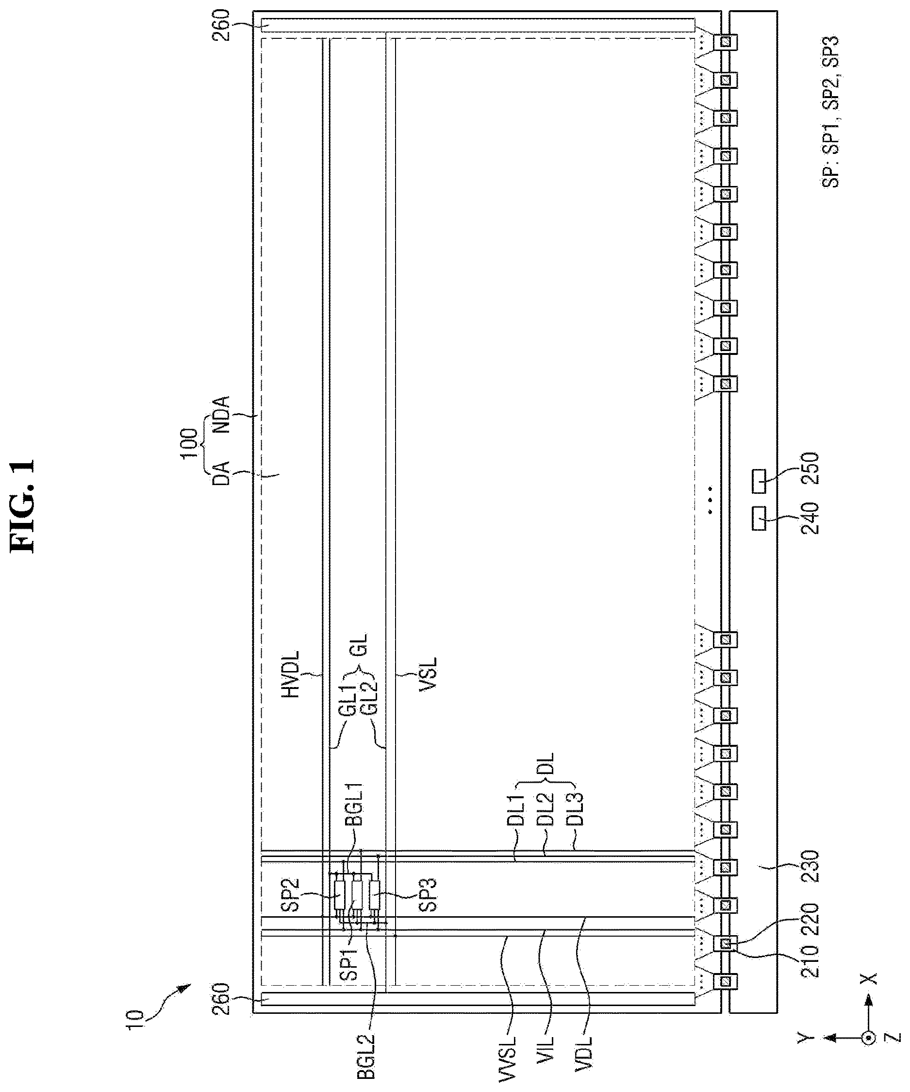
is a plan view illustrating a display device according to an embodiment.
The terms “above”, “top”, and “upper surface” as used herein refer to an upward direction (i.e., a Z-axis direction) with respect to the display device. The terms “below”, “bottom”, and “lower surface” as used herein refer to a downward direction (i.e., a direction opposite to the Z axis direction) with respect to the display device. In addition, “left side”, “right side”, “upper side”, and “lower side” refer to directions when the display device is viewed from above. For example, “left side” refers to a direction opposite to an X-axis direction, “right side” refers to the X-axis direction, “upper side” refers to a Y-axis direction, and “lower side” refers to a direction opposite to the Y-axis direction.
Referring to , a display device 10 may be a device that displays a moving image or a still image, and may be used as a display screen of various products such as televisions, laptop computers, monitors, billboards, and Internet of Things (IOT) as well as portable electronic devices such as mobile phones, smartphones, tablet personal computers (PCs), smart watches, watch phones, mobile communication terminals, electronic organizers, electronic books, portable multimedia players (PMPs), navigation devices, and ultra mobile PCs (UMPCs).
The display device 10 may include a display panel 100 , flexible films 210 , display drivers 220 , a circuit board 230 , a timing controller 240 , a power supply unit 250 , and gate drivers 260 .
The display panel 100 may have a rectangular shape in plan view. For example, the display panel 100 may have a rectangular shape, in plan view, having long sides in a first direction (e.g., X-axis direction) and short sides in a second direction (e.g., Y-axis direction). A corner where the long side in the first direction (e.g., X-axis direction) and the short side in the second direction (e.g., Y-axis direction) meet may be right-angled or may be rounded with a certain curvature. The shape of the display panel 100 in plan view is not limited to the rectangular shape, and may be other polygonal shapes, a circular shape, or an elliptical shape. As an example, the display panel 100 may be formed to be flat, but embodiments are not limited thereto. As another example, the display panel 100 may be formed to be bent with a certain curvature.
The display panel 100 may include a display area DA and a non-display area NDA.
The display area DA may be an area displaying an image, and may be defined as a central area of the display panel 100 . The display area DA may include pixels SP, gate lines GL, data lines DL, initialization voltage lines VIL, first voltage lines VDL, horizontal voltage lines HVDL, vertical voltage lines VVSL, and second voltage lines VSL. The pixels SP may be formed in each of pixel areas crossed by the data lines DL and the gate lines GL. The pixel SP may include first to third pixels SP 1 , SP 2 , and SP 3 . Each of the first to third pixels SP 1 , SP 2 , and SP 3 may be connected to the gate line GL and the data line DL. Each of the first to third pixels SP 1 , SP 2 , and SP 3 may be defined as an area of a minimum unit emitting light.
Each of the first to third pixels SP 1 , SP 2 , and SP 3 may include an organic light emitting diode including an organic light emitting layer, a quantum dot light emitting diode including a quantum dot light emitting layer, a micro light emitting diode, or an inorganic light emitting diode including an inorganic semiconductor.
The first pixel SP 1 may emit light of a first color or red light, the second pixel SP 2 may emit light of a second color or green light, and the third pixel SP 3 may emit light of a third color or blue light. A pixel circuit of the second pixel SP 2 , a pixel circuit of the first pixel SP 1 , and a pixel circuit of the third pixel SP 3 may be arranged in a direction opposite to the second direction (e.g., Y-axis direction), but the order of the pixel circuits is not limited thereto.
The gate lines GL may include first gate lines GL 1 and second gate lines GL 2 . The first gate lines GL 1 may extend in the first direction (e.g., X-axis direction) and may be spaced apart from each other in the second direction (e.g., Y-axis direction). The first gate lines GL 1 may receive first gate signals from the gate drivers 260 and supply the first gate signals to first auxiliary gate lines BGL 1 . The first auxiliary gate lines BGL 1 may extend from the first gate lines GL 1 and supply the first gate signals to the first to third pixels SP 1 , SP 2 , and SP 3 .
The second gate lines GL 2 may extend in the first direction (e.g., X-axis direction) and may be spaced apart from each other in the second direction (e.g., Y-axis direction). The second gate lines GL 2 may receive second gate signals from the gate drivers 260 and supply the second gate signals to second auxiliary gate lines BGL 2 . The second auxiliary gate lines BGL 2 may extend from the second gate lines GL 2 and supply the second gate signals to the first to third pixels SP 1 , SP 2 , and SP 3 .
The data lines DL may extend in the second direction (e.g., Y-axis direction) and may be spaced apart from each other in the first direction (e.g., X-axis direction). The data lines DL may include first to third data lines DL 1 , DL 2 , and DL 3 . Each of the first to third data lines DL 1 , DL 2 , and DL 3 may supply a data voltage to each of the first to third pixels SP 1 , SP 2 , and SP 3 .
The initialization voltage lines VIL may extend in the second direction (e.g., Y-axis direction) and may be spaced apart from each other in the first direction (e.g., X-axis direction). The initialization voltage lines VIL may supply initialization voltages received from the display drivers 220 to the pixel circuit of each of the first to third pixels SP 1 , SP 2 , and SP 3 . The initialization voltage lines VIL may receive sensed signals from the pixel circuit of each of the first to third pixels SP 1 , SP 2 , and SP 3 and supply the sensed signals to the display drivers 220 .
The first voltage lines VDL may extend in the second direction (e.g., Y-axis direction) and may be spaced apart from each other in the first direction (e.g., X-axis direction). The first voltage lines VDL may supply driving voltages or high potential voltages received from the power supply unit 250 to the first to third pixels SP 1 , SP 2 , and SP 3 .
The horizontal voltage lines HVDL may extend in the first direction (e.g., X-axis direction) and may be spaced apart from each other in the second direction (e.g., Y-axis direction). The horizontal voltage lines HVDL may be connected to the first voltage lines VDL. The horizontal voltage lines HVDL may receive the driving voltages or the high potential voltages from the first voltage lines VDL.
The vertical voltage lines VVSL may extend in the second direction (e.g., Y-axis direction) and may be spaced apart from each other in the first direction (e.g., X-axis direction). The vertical voltage lines VVSL may be connected to the second voltage lines VSL. The vertical voltage lines VVSL may supply low potential voltages received from the power supply unit 250 to the second voltage lines VSL.
The second voltage lines VSL may extend in the first direction (e.g., X-axis direction) and may be spaced apart from each other in the second direction (e.g., Y-axis direction). The second voltage lines VSL may supply the low potential voltages to the first to third pixels SP 1 , SP 2 , and SP 3 .
Connection structures/relationships between the pixels SP, the gate lines GL, the data lines DL, the initialization voltage lines VIL, the first voltage lines VDL, and the second voltage lines VSL may be designed and changed according to the number and an arrangement of pixels SP.
The non-display area NDA may be defined as an area other than the display area DA in the display panel 100 . For example, the non-display area NDA may include fan-out lines connecting the data lines DL, the initialization voltage lines VIL, the first voltage lines VDL, and the vertical voltage lines VVSL to the display drivers 220 , the gate drivers 260 , and pad parts connected to the flexible films 210 .
The flexible films 210 may be connected to the pad parts disposed on the lower side of the non-display area NDA. Input terminals provided on one sides of the flexible films 210 may be attached to the circuit board 230 by a film attaching process, and output terminals provided on the other sides of the flexible films 210 may be attached to the pad parts by a film attaching process. For example, the flexible films 210 may be bent like a tape carrier package or a chip on film. The flexible films 210 may be bent below the display panel 100 in order to decrease a bezel area of the display device 10 .
The display drivers 220 may be mounted on the flexible films 210 . For example, the display driver 220 may be implemented as an integrated circuit (IC). The display drivers 220 may receive digital video data and data control signals from the timing controller 240 , convert the digital video data into analog data voltages according to the data control signals, and supply the analog data voltages to the data lines DL through the fan-out lines.
The circuit board 230 may support the timing controller 240 and the power supply unit 250 , and supply signals and power to the display drivers 220 . For example, the circuit board 230 may supply signals supplied from the timing controller 240 and source voltages supplied from the power supply unit 250 to the flexible films 210 and the display drivers 220 in order to display an image in each pixel. For example, signal lines and power lines may be provided on the circuit board 230 .
The timing controller 240 may be mounted on the circuit board 230 and may receive image data and timing synchronization signals supplied from a display driving system or a graphic device through a user connector provided on the circuit board 230 . The timing controller 240 may generate the digital video data by aligning the image data to be suitable for a pixel arrangement structure based on the timing synchronization signals, and may supply the generated digital video data to the display drivers 220 . The timing controller 240 may generate data control signals and gate control signals based on the timing synchronization signals. The timing controller 240 may control a supply timing of data voltages of the display drivers 220 based on the data control signals, and may control a supply timing of gate signals of the gate drivers 260 based on the gate control signals.
The power supply unit 250 may be disposed on the circuit board 230 and may supply source voltages to the flexible films 210 and the display drivers 220 . For example, the power supply unit 250 may generate driving voltages or high potential voltages and supply the driving voltages or the high potential voltages to the first voltage lines VDL, may generate low potential voltages and supply the low potential voltages to the vertical voltage lines VVSL, and may generate initialization voltages and supply the initialization voltages to the initialization voltage lines VIL.
The gate drivers 260 may be disposed on the left and right sides of the non-display area NDA. The gate drivers 260 may generate gate signals based on the gate control signals supplied from the timing controller 240 . The gate control signals may include start signals, clock signals, and source voltages, but embodiments are not limited thereto. The gate drivers 260 may supply the gate signals to the gate lines GL according to a set order.
is a schematic view illustrating pixels and lines of the display device according to an embodiment.
Referring to , the pixel SP may include first to third pixels SP 1 , SP 2 , and SP 3 . A pixel circuit of the second pixel SP 2 , a pixel circuit of the first pixel SP 1 , and a pixel circuit of the third pixel SP 3 may be arranged in the direction opposite to the second direction (e.g., Y-axis direction), but the order of the pixel circuits is not limited thereto.
Each of the first to third pixels SP 1 , SP 2 , and SP 3 may be connected to the first voltage line VDL, the initialization voltage line VIL, the gate line GL, and the data line DL.
The first voltage line VDL may extend in the second direction (e.g., Y-axis direction). The first voltage line VDL may be disposed on the left side of the pixel circuits of the first to third pixels SP 1 , SP 2 , and SP 3 . The first voltage line VDL may supply the driving voltage or the high potential voltage to a transistor of each of the first to third pixels SP 1 , SP 2 , and SP 3 .
The horizontal voltage line HVDL may extend in the first direction (e.g., X-axis direction). The horizontal voltage line HVDL may be disposed on the upper side of a first gate line GL 1 disposed in a k-th row ROWk (here, k is a positive integer). The horizontal voltage line HVDL may be connected to the first voltage line VDL. The horizontal voltage line HVDL may receive the driving voltage or the high potential voltage from the first voltage line VDL.
The initialization voltage line VIL may extend in the second direction (e.g., Y-axis direction). The initialization voltage line VIL may be disposed on the left side of the second auxiliary gate line BGL 2 . The initialization voltage line VIL may be disposed between the vertical voltage line VVSL and the second auxiliary gate line BGL 2 . The initialization voltage line VIL may supply the initialization voltage to the pixel circuit of each of the first to third pixels SP 1 , SP 2 , and SP 3 . The initialization voltage line VIL may receive a sensed signal from the pixel circuit of each of the first to third pixels SP 1 , SP 2 , and SP 3 and supply the sensed signal to the display driver 220 .
The vertical voltage line VVSL may extend in the second direction (e.g., Y-axis direction). The vertical voltage line VVSL may be disposed on the left side of the initialization voltage line VIL. The vertical voltage line VVSL may be connected between the power supply unit 250 and the second voltage line VSL. The vertical voltage line VVSL may supply the low potential voltage supplied from the power supply unit 250 to the second voltage line VSL.
The second voltage line VSL may extend in the first direction (e.g., X-axis direction). The second voltage line VSL may be disposed on the upper side of a first gate line GL 1 disposed in a (k+1)-th row ROWk+1. The second voltage line VSL may supply the low potential voltage received from the vertical voltage line VVSL to light emitting element layers of the first to third pixels SP 1 , SP 2 , and SP 3 .
The first gate line GL 1 may extend in the first direction (e.g., X-axis direction). The first gate line GL 1 may be disposed on the upper side of the pixel circuit of the second pixel SP 2 . The first gate line GL 1 may supply the first gate signal received from the gate driver 260 to the first auxiliary gate line BGL 1 . The first auxiliary gate line BGL 1 may extend from the first gate line GL 1 in the direction opposite to the second direction (e.g., Y-axis direction). The first auxiliary gate line BGL 1 may be disposed on the right side of the pixel circuits of the first to third pixels SP 1 , SP 2 , and SP 3 . The first auxiliary gate line BGL 1 may supply the first gate signal received from the first gate line GL 1 to the pixel circuits of the first to third pixels SP 1 , SP 2 , and SP 3 .
The second gate line GL 2 may extend in the first direction (e.g., X-axis direction). The second gate line GL 2 may be disposed on the lower side of the pixel circuit of the third pixel SP 3 . The second gate line GL 2 may supply the second gate signal received from the gate driver 260 to the second auxiliary gate line BGL 2 . The second auxiliary gate line BGL 2 may extend from the second gate line GL 2 in the second direction (e.g., Y-axis direction). The second auxiliary gate line BGL 2 may be disposed on the left side of the first voltage line VDL. The second auxiliary gate line BGL 2 may supply the second gate signal received from the second gate line GL 2 to the pixel circuits of the first to third pixels SP 1 , SP 2 , and SP 3 .
The data lines DL may extend in the second direction (e.g., Y-axis direction). The data lines DL may supply the data voltages to the pixels SP. The data lines DL may include first to third data lines DL 1 , DL 2 , and DL 3 .
The first data line DL 1 may extend in the second direction (e.g., Y-axis direction). The first data line DL 1 may be disposed on the right side of the first auxiliary gate line BGL 1 . The first data line DL 1 may supply the data voltage received from the display driver 220 to the pixel circuit of the first pixel SP 1 .
The second data line DL 2 may extend in the second direction (e.g., Y-axis direction). The second data line DL 2 may be disposed on the right side of the first data line DL 1 . The second data line DL 2 may supply the data voltage received from the display driver 220 to the pixel circuit of the second pixel SP 2 .
The third data line DL 3 may extend in the second direction (e.g., Y-axis direction). The third data line DL 3 may be disposed on the right side of the second data line DL 2 . The third data line DL 3 may supply the data voltage received from the display driver 220 to the pixel circuit of the third pixel SP 3 .
is a schematic diagram of an equivalent circuit illustrating a pixel of the display device according to an embodiment.
Referring to , each of the pixels SP may be connected to a first voltage line VDL, a data line DL, an initialization voltage line VIL, a first gate line GL 1 , a second gate line GL 2 , and a vertical voltage line VVSL.
Each of the first to third pixels SP 1 , SP 2 , and SP 3 may include a pixel circuit and a plurality of light emitting elements ED. The pixel circuit of each of the first to third pixels SP 1 , SP 2 , and SP 3 may include first to third transistors ST 1 , ST 2 , and ST 3 and a first capacitor C 1 .
The first transistor ST 1 may include a gate electrode, a drain electrode, and a source electrode. The gate electrode of the first transistor ST 1 may be connected to a first node N 1 , the drain electrode of the first transistor ST 1 may be connected to the first voltage line VDL, and the source electrode of the first transistor ST 1 may be connected to a second node N 2 . The first transistor ST 1 may control a drain-source current (or a driving current) based on a data voltage applied to the gate electrode.
The light emitting elements ED may include first and second light emitting elements ED 1 and ED 2 . The first and second light emitting elements ED 1 and ED 2 may be connected to each other in series. The first and second light emitting elements ED 1 and ED 2 may receive the driving current to emit light. A light emission amount or luminance of the light emitting element ED may be proportional to a magnitude of the driving current. The light emitting element ED may be an organic light emitting diode including an organic light emitting layer, a quantum dot light emitting diode including a quantum dot light emitting layer, a micro light emitting diode, or an inorganic light emitting diode including an inorganic semiconductor.
A first electrode of the first light emitting element ED 1 may be connected to the second node N 2 , and a second electrode of the first light emitting element ED 1 may be connected to a third node N 3 . The first electrode of the first light emitting element ED 1 may be connected to the source electrode of the first transistor ST 1 , a drain electrode of the third transistor ST 3 , and a second capacitor electrode of the first capacitor C 1 through the second node N 2 . The second electrode of the first light emitting element ED 1 may be connected to a first electrode of the second light emitting element ED 2 through the third node N 3 .
The first electrode of the second light emitting element ED 2 may be connected to the third node N 3 , and a second electrode of the second light emitting element ED 2 may be connected to the vertical voltage line VVSL.
The second transistor ST 2 may be turned on by a first gate signal of the first gate line GL 1 to electrically connect the data line DL and the first node N 1 , which is the gate electrode of the first transistor ST 1 , to each other. The second transistor ST 2 may be turned on based on the first gate signal to supply a data voltage to the first node N 1 . A gate electrode of the second transistor ST 2 may be connected to the first gate line GL 1 , a drain electrode of the second transistor ST 2 may be connected to the data line DL, and a source electrode of the second transistor ST 2 may be connected to the first node N 1 . The source electrode of the second transistor ST 2 may be connected to the gate electrode of the first transistor ST 1 and a first capacitor electrode of the first capacitor C 1 through the first node N 1 .
The third transistor ST 3 may be turned on by a second gate signal of the second gate line GL 2 to electrically connect the initialization voltage line VIL and the second node N 2 , which is the source electrode of the first transistor ST 1 , to each other. The third transistor ST 3 may be turned on based on the second gate signal to supply an initialization voltage to the second node N 2 . The third transistor ST 3 may be turned on based on the second gate signal to supply a sensed signal to the initialization voltage line VIL. A gate electrode of the third transistor ST 3 may be connected to the second gate line GL 2 , the drain electrode of the third transistor ST 3 may be connected to the second node N 2 , and a source electrode of the third transistor ST 3 may be connected to the initialization voltage line VIL. The drain electrode of the third transistor ST 3 may be connected to the source electrode of the first transistor ST 1 , the second capacitor electrode of the first capacitor C 1 , and the first electrode of the first light emitting element ED 1 through the second node N 2 .
is a schematic plan view illustrating a thin film transistor layer of the display device of , and is a schematic cross-sectional view taken along line I-I′ of .
Referring to , the display area DA may include first to third pixels SP 1 , SP 2 , and SP 3 , a first voltage line VDL, a horizontal voltage line HVDL, an initialization voltage line VIL, first and second gate lines GL 1 and GL 2 , first and second auxiliary gate lines BGL 1 and BGL 2 , a data line DL, a second voltage line VSL, and a vertical voltage line VVSL.
The pixel SP may include first to third pixels SP 1 , SP 2 , and SP 3 . A pixel circuit of the second pixel SP 2 , a pixel circuit of the first pixel SP 1 , and a pixel circuit of the third pixel SP 3 may be arranged in the direction opposite to the second direction (e.g., Y-axis direction), but the order of the pixel circuits is not limited thereto.
The first voltage line VDL may be disposed at (or formed as) a first metal layer MTL 1 on a substrate SUB. The first voltage line VDL may be disposed on the left side of the pixel circuits of the first to third pixels SP 1 , SP 2 , and SP 3 . The first voltage line VDL may overlap a first auxiliary electrode AUE 1 of a second metal layer MTL 2 and a second auxiliary electrode AUE 2 of a third metal layer MTL 3 . The second metal layer MTL 2 may be disposed on a gate insulating layer GI covering an active layer ACTL, and the third metal layer MTL 3 may be disposed on an interlayer insulating layer ILD covering the second metal layer MTL 2 . A passivation layer PV may cover the third metal layer MTL 3 . The first auxiliary electrode AUE 1 may be connected to the first voltage line VDL. The second auxiliary electrode AUE 2 may be connected to the first auxiliary electrode AUE 1 . The first voltage line VDL may be connected to the first and second auxiliary electrodes AUE 1 and AUE 2 to decrease line resistance.
The second auxiliary electrode AUE 2 may be connected to a drain electrode DE 1 of a first transistor ST 1 of each of the first to third pixels SP 1 , SP 2 , and SP 3 . Accordingly, the first voltage line VDL may supply the driving voltage to the first to third pixels SP 1 , SP 2 , and SP 3 through the second auxiliary electrode AUE 2 .
The horizontal voltage line HVDL may be disposed at (or formed as) the third metal layer MTL 3 . The horizontal voltage line HVDL may be disposed on the upper side of the first gate line GL 1 . The horizontal voltage line HVDL may be connected to the first voltage line VDL to receive the driving voltage.
The initialization voltage line VIL may be disposed at (or formed as) the first metal layer MTL 1 . The initialization voltage line VIL may be disposed on the left side of the first voltage line VDL. The initialization voltage line VIL may overlap a fifth auxiliary electrode AUE 5 of the third metal layer MTL 3 and may be connected to the fifth auxiliary electrode AUE 5 . The initialization voltage line VIL may be connected to the fifth auxiliary electrode AUE 5 to decrease line resistance.
The fifth auxiliary electrode AUE 5 may be connected to a source electrode SE 3 of a third transistor ST 3 of each of the first to third pixels SP 1 , SP 2 , and SP 3 . Accordingly, the initialization voltage line VIL may supply the initialization voltage to the third transistor ST 3 of each of the first to third pixels SP 1 , SP 2 , and SP 3 and receive the sensed signal from the third transistor ST 3 of each of the first to third pixels SP 1 , SP 2 , and SP 3 , through the fifth auxiliary electrode AUE 5 .
The vertical voltage line VVSL may be disposed at (or formed as) the first metal layer MTL 1 . The vertical voltage line VVSL may be disposed on the left side of the initialization voltage line VIL. The vertical voltage line VVSL may overlap a third auxiliary electrode AUE 3 of the second metal layer MTL 2 and a fourth auxiliary electrode AUE 4 of the third metal layer MTL 3 . The third auxiliary electrode AUE 3 may be connected to the vertical voltage line VVSL, and the fourth auxiliary electrode AUE 4 may be connected to the third auxiliary electrode AUE 3 . The vertical voltage line VVSL may be connected to the third and fourth auxiliary electrodes AUE 3 and AUE 4 to decrease line resistance. The vertical voltage line VVSL may be connected to the second voltage line VSL to supply the low potential voltage to the second voltage line VSL.
The second voltage line VSL may be disposed at (or formed as) the third metal layer MTL 3 . The second voltage line VSL may be disposed on the lower side of the second gate line GL 2 . The second voltage line VSL may receive the low potential voltage from the vertical voltage line VVSL.
The first gate line GL 1 may be disposed at (or formed as) the third metal layer MTL 3 . The first gate line GL 1 may be disposed on the upper side of the pixel circuit of the second pixel SP 2 . The first gate line GL 1 may be connected to the first auxiliary gate line BGL 1 and may supply the first gate signal received from the gate driver 260 to the first auxiliary gate line BGL 1 .
The first auxiliary gate line BGL 1 may be disposed at (or formed as) the second metal layer MTL 2 . The first auxiliary gate line BGL 1 may protrude from the first gate line GL 1 in the direction opposite to the second direction (e.g., Y-axis direction). The first auxiliary gate line BGL 1 may be disposed on the right side of the pixel circuits of the first to third pixels SP 1 , SP 2 , and SP 3 . The first auxiliary gate line BGL 1 may supply the first gate signal received from the first gate line GL 1 to a second transistor ST 2 of each of the first to third pixels SP 1 , SP 2 , and SP 3 .
The second gate line GL 2 may be disposed at (or formed as) the third metal layer MTL 3 . The second gate line GL 2 may be disposed on the lower side of the pixel circuit of the third pixel SP 3 . The second gate line GL 2 may be connected to the second auxiliary gate line BGL 2 and may supply the second gate signal received from the gate driver 260 to the second auxiliary gate line BGL 2 .
The second auxiliary gate line BGL 2 may be disposed at (or formed as) the second metal layer MTL 2 . The second auxiliary gate line BGL 2 may protrude from the second gate line GL 2 in the second direction (e.g., Y-axis direction). The second auxiliary gate line BGL 2 may be disposed between the initialization voltage line VIL and the first voltage line VDL. The second auxiliary gate line BGL 2 may supply the second gate signal received from the second gate line GL 2 to the third transistor ST 3 of each of the first to third pixels SP 1 , SP 2 , and SP 3 .
The first data line DL 1 may be disposed at (or formed as) the first metal layer MTL 1 . The first data line DL 1 may be disposed on the right side of the first auxiliary gate line BGL 1 . A second connection electrode CE 2 of the third metal layer MTL 3 may electrically connect the first data line DL 1 and a drain electrode DE 2 of the second transistor ST 2 of the first pixel SP 1 to each other. Accordingly, the first data line DL 1 may supply the data voltage to the second transistor ST 2 of the first pixel SP 1 through the second connection electrode CE 2 .
The second data line DL 2 may be disposed at (or formed as) the first metal layer MTL 1 . The second data line DL 2 may be disposed on the right side of the first data line DL 1 . A fifth connection electrode CE 5 of the third metal layer MTL 3 may electrically connect the second data line DL 2 and a drain electrode DE 2 of the second transistor ST 2 of the second pixel SP 2 to each other. Accordingly, the second data line DL 2 may supply the data voltage to the second transistor ST 2 of the second pixel SP 2 through the fifth connection electrode CE 5 .
The third data line DL 3 may be disposed at (or formed as) the first metal layer MTL 1 . The third data line DL 3 may be disposed on the right side of the second data line DL 2 . An eighth connection electrode CE 8 of the third metal layer MTL 3 may electrically connect the third data line DL 3 and a drain electrode DE 2 of the second transistor ST 2 of the third pixel SP 3 to each other. Accordingly, the third data line DL 3 may supply the data voltage to the second transistor ST 2 of the third pixel SP 3 through the eighth connection electrode CE 8 .
The pixel circuit of the first pixel SP 1 may include first to third transistors ST 1 , ST 2 , and ST 3 . The first transistor ST 1 of the first pixel SP 1 may include an active region ACT 1 , a gate electrode GE 1 , the drain electrode DE 1 , and a source electrode SE 1 . The active region ACT 1 of the first transistor ST 1 may be disposed at (or formed as) the active layer ACTL, and may overlap the gate electrode GE 1 of the first transistor ST 1 . The active layer ACTL may be disposed on a buffer layer BF covering the first metal layer MTL 1 .
The gate electrode GE 1 of the first transistor ST 1 may be disposed at (or formed as) the second metal layer MTL 2 . The gate electrode GE 1 of the first transistor ST 1 may be a portion of a first capacitor electrode CPE 1 of a first capacitor C 1 .
The drain electrode DE 1 and the source electrode SE 1 of the first transistor ST 1 may be made to be conductive by heat-treating the active layer ACTL. The drain electrode DE 1 and the source electrode SE 1 may be made to be conductive as N-type semiconductors, but embodiments are not limited thereto. The drain electrode DE 1 of the first transistor ST 1 may be electrically connected to the first voltage line VDL through the second auxiliary electrode AUE 2 . The drain electrode DE 1 of the first transistor ST 1 may receive the driving voltage from the first voltage line VDL.
The source electrode SE 1 of the first transistor ST 1 may be connected to a first connection electrode CE 1 of the third metal layer MTL 3 . The first connection electrode CE 1 may be connected to a second capacitor electrode CPE 2 of the first metal layer MTL 1 . Accordingly, the first capacitor C 1 may be doubly formed between the first capacitor electrode CPE 1 and the second capacitor electrode CPE 2 and between the first capacitor electrode CPE 1 and the first connection electrode CE 1 .
The first connection electrode CE 1 may be electrically connected to a light emitting element ED of the first pixel SP 1 . Accordingly, the first connection electrode CE 1 may supply the driving current received from the pixel circuit of the first pixel SP 1 to the light emitting element ED.
The second transistor ST 2 of the first pixel SP 1 may include an active region ACT 2 , a gate electrode GE 2 , the drain electrode DE 2 , and a source electrode SE 2 . The active region ACT 2 of the second transistor ST 2 may be disposed at (or formed as) the active layer ACTL, and may overlap the gate electrode GE 2 of the second transistor ST 2 .
The gate electrode GE 2 of the second transistor ST 2 may be disposed at (or formed as) the second metal layer MTL 2 . The gate electrode GE 2 of the second transistor ST 2 may be a portion of the first auxiliary gate line BGL 1 .
The drain electrode DE 2 and the source electrode SE 2 of the second transistor ST 2 may be made to be conductive by heat-treating the active layer ACTL. The drain electrode DE 2 of the second transistor ST 2 may be electrically connected to the first data line DL 1 through the second connection electrode CE 2 . Accordingly, the first data line DL 1 may supply the data voltage to the second transistor ST 2 of the first pixel SP 1 through the second connection electrode CE 2 . The source electrode SE 2 of the second transistor ST 2 may be electrically connected to the first capacitor electrode CPE 1 of the first capacitor C 1 through a third connection electrode CE 3 of the third metal layer MTL 3 .
The third transistor ST 3 of the first pixel SP 1 may include an active region ACT 3 , a gate electrode GE 3 , a drain electrode DE 3 , and the source electrode SE 3 . The active region ACT 3 of the third transistor ST 3 may be disposed at (or formed as) the active layer ACTL, and may overlap the gate electrode GE 3 of the third transistor ST 3 .
The gate electrode GE 3 of the third transistor ST 3 may be disposed at (or formed as) the second metal layer MTL 2 . The gate electrode GE 3 of the third transistor ST 3 may be a portion of the second auxiliary gate line BGL 2 .
The drain electrode DE 3 and the source electrode SE 3 of the third transistor ST 3 may be made to be conductive by heat-treating the active layer ACTL. The drain electrode DE 3 of the third transistor ST 3 may be connected to an extension part of the first connection electrode CE 1 . The drain electrode DE 3 of the third transistor ST 3 may be electrically connected to the source electrode SE 1 of the first transistor ST 1 and the second capacitor electrode CPE 2 of the first capacitor C 1 through the first connection electrode CE 1 .
The source electrode SE 3 of the third transistor ST 3 may be electrically connected to the initialization voltage line VIL through the fifth auxiliary electrode AUE 5 . The source electrode SE 3 of the third transistor ST 3 may receive the initialization voltage from the initialization voltage line VIL. The source electrode SE 3 of the third transistor ST 3 may supply the sensed signal to the initialization voltage line VIL.
The pixel circuit of the second pixel SP 2 may include first to third transistors ST 1 , ST 2 , and ST 3 . The first transistor ST 1 of the second pixel SP 2 may include an active region ACT 1 , a gate electrode GE 1 , the drain electrode DE 1 , and a source electrode SE 1 . The active region ACT 1 of the first transistor ST 1 may be disposed at (or formed as) the active layer ACTL, and may overlap the gate electrode GE 1 of the first transistor ST 1 .
The gate electrode GE 1 of the first transistor ST 1 may be disposed at (or formed as) the second metal layer MTL 2 . The gate electrode GE 1 of the first transistor ST 1 may be a portion of a first capacitor electrode CPE 1 of a first capacitor C 1 .
The drain electrode DE 1 and the source electrode SE 1 of the first transistor ST 1 may be made to be conductive by heat-treating the active layer ACTL. The drain electrode DE 1 and the source electrode SE 1 may be made to be conductive as N-type semiconductors, but embodiments are not limited thereto. The drain electrode DE 1 of the first transistor ST 1 may be electrically connected to the first voltage line VDL through the second auxiliary electrode AUE 2 . The drain electrode DE 1 of the first transistor ST 1 may receive the driving voltage from the first voltage line VDL.
The source electrode SE 1 of the first transistor ST 1 may be connected to a fourth connection electrode CE 4 of the third metal layer MTL 3 . The fourth connection electrode CE 4 may be connected to a second capacitor electrode CPE 2 of the first metal layer MTL 1 . Accordingly, the first capacitor C 1 may be doubly formed between the first capacitor electrode CPE 1 and the second capacitor electrode CPE 2 and between the first capacitor electrode CPE 1 and the fourth connection electrode CE 4 .
The fourth connection electrode CE 4 may be electrically connected to a light emitting element ED of the second pixel SP 2 . Accordingly, the fourth connection electrode CE 4 may supply the driving current received from the pixel circuit of the second pixel SP 2 to the light emitting element ED.
The second transistor ST 2 of the second pixel SP 2 may include an active region ACT 2 , a gate electrode GE 2 , the drain electrode DE 2 , and a source electrode SE 2 . The active region ACT 2 of the second transistor ST 2 may be disposed at (or formed as) the active layer ACTL, and may overlap the gate electrode GE 2 of the second transistor ST 2 .
The gate electrode GE 2 of the second transistor ST 2 may be disposed at (or formed as) the second metal layer MTL 2 . The gate electrode GE 2 of the second transistor ST 2 may be a portion of the first auxiliary gate line BGL 1 .
The drain electrode DE 2 and the source electrode SE 2 of the second transistor ST 2 may be made to be conductive by heat-treating the active layer ACTL. The drain electrode DE 2 of the second transistor ST 2 may be electrically connected to the second data line DL 2 through the fifth connection electrode CE 5 . Accordingly, the second data line DL 2 may supply the data voltage to the second transistor ST 2 of the second pixel SP 2 through the fifth connection electrode CE 5 . The source electrode SE 2 of the second transistor ST 2 may be electrically connected to the first capacitor electrode CPE 1 of the first capacitor C 1 through a sixth connection electrode CE 6 of the third metal layer MTL 3 .
The third transistor ST 3 of the second pixel SP 2 may include an active region ACT 3 , a gate electrode GE 3 , a drain electrode DE 3 , and the source electrode SE 3 . The active region ACT 3 of the third transistor ST 3 may be disposed at (or formed as) the active layer ACTL, and may overlap the gate electrode GE 3 of the third transistor ST 3 .
The gate electrode GE 3 of the third transistor ST 3 may be disposed at (or formed as) the second metal layer MTL 2 . The gate electrode GE 3 of the third transistor ST 3 may be a portion of the second auxiliary gate line BGL 2 .
The drain electrode DE 3 and the source electrode SE 3 of the third transistor ST 3 may be made to be conductive by heat-treating the active layer ACTL. The drain electrode DE 3 of the third transistor ST 3 may be connected to an extension part of the fourth connection electrode CE 4 . The drain electrode DE 3 of the third transistor ST 3 may be electrically connected to the source electrode SE 1 of the first transistor ST 1 and the second capacitor electrode CPE 2 of the first capacitor C 1 through the fourth connection electrode CE 4 .
The source electrode SE 3 of the third transistor ST 3 may be electrically connected to the initialization voltage line VIL through the fifth auxiliary electrode AUE 5 . The source electrode SE 3 of the third transistor ST 3 may receive the initialization voltage from the initialization voltage line VIL. The source electrode SE 3 of the third transistor ST 3 may supply the sensed signal to the initialization voltage line VIL.
The pixel circuit of the third pixel SP 3 may include first to third transistors ST 1 , ST 2 , and ST 3 . The first transistor ST 1 of the third pixel SP 3 may include an active region ACT 1 , a gate electrode GE 1 , the drain electrode DE 1 , and a source electrode SEL. The active region ACT 1 of the first transistor ST 1 may be disposed at (or formed as) the active layer ACTL, and may overlap the gate electrode GE 1 of the first transistor ST 1 .
The gate electrode GE 1 of the first transistor ST 1 may be disposed at (or formed as) the second metal layer MTL 2 . The gate electrode GE 1 of the first transistor ST 1 may be a portion of a first capacitor electrode CPE 1 of a first capacitor C 1 .
The drain electrode DE 1 and the source electrode SE 1 of the first transistor ST 1 may be made to be conductive by heat-treating the active layer ACTL. The drain electrode DE 1 and the source electrode SE 1 may be made to be conductive as N-type semiconductors, but embodiments are not limited thereto. The drain electrode DE 1 of the first transistor ST 1 may be electrically connected to the first voltage line VDL through the second auxiliary electrode AUE 2 . The drain electrode DE 1 of the first transistor ST 1 may receive the driving voltage from the first voltage line VDL.
The source electrode SE 1 of the first transistor ST 1 may be connected to a seventh connection electrode CE 7 of the third metal layer MTL 3 . The seventh connection electrode CE 7 may be connected to a second capacitor electrode CPE 2 of the first metal layer MTL 1 . Accordingly, the first capacitor C 1 may be doubly formed between the first capacitor electrode CPE 1 and the second capacitor electrode CPE 2 and between the first capacitor electrode CPE 1 and the seventh connection electrode CE 7 .
The seventh connection electrode CE 7 may be electrically connected to a light emitting element ED of the third pixel SP 3 . Accordingly, the seventh connection electrode CE 7 may supply the driving current received from the pixel circuit of the third pixel SP 3 to the light emitting element ED.
The second transistor ST 2 of the third pixel SP 2 may include an active region ACT 2 , a gate electrode GE 2 , the drain electrode DE 2 , and a source electrode SE 2 . The active region ACT 2 of the second transistor ST 2 may be disposed at (or formed as) the active layer ACTL, and may overlap the gate electrode GE 2 of the second transistor ST 2 .
The gate electrode GE 2 of the second transistor ST 2 may be disposed at (or formed as) the second metal layer MTL 2 . The gate electrode GE 2 of the second transistor ST 2 may be a portion of the first auxiliary gate line BGL 1 .
The drain electrode DE 2 and the source electrode SE 2 of the second transistor ST 2 may be made to be conductive by heat-treating the active layer ACTL. The drain electrode DE 2 of the second transistor ST 2 may be electrically connected to the third data line DL 3 through the eighth connection electrode CE 8 . Accordingly, the third data line DL 3 may supply the data voltage to the second transistor ST 2 of the third pixel SP 3 through the eighth connection electrode CE 8 . The source electrode SE 2 of the second transistor ST 2 may be electrically connected to the first capacitor electrode CPE 1 of the first capacitor C 1 through a ninth connection electrode CE 9 of the third metal layer MTL 3 .
The third transistor ST 3 of the third pixel SP 3 may include an active region ACT 3 , a gate electrode GE 3 , a drain electrode DE 3 , and the source electrode SE 3 . The active region ACT 3 of the third transistor ST 3 may be disposed at (or formed as) the active layer ACTL, and may overlap the gate electrode GE 3 of the third transistor ST 3 .
The gate electrode GE 3 of the third transistor ST 3 may be disposed at (or formed as) the second metal layer MTL 2 . The gate electrode GE 3 of the third transistor ST 3 may be a portion of the second auxiliary gate line BGL 2 .
The drain electrode DE 3 and the source electrode SE 3 of the third transistor ST 3 may be made to be conductive by heat-treating the active layer ACTL. The drain electrode DE 3 of the third transistor ST 3 may be connected to a second extension part of the seventh connection electrode CE 7 . The drain electrode DE 3 of the third transistor ST 3 may be electrically connected to the source electrode SE 1 of the first transistor ST 1 and the second capacitor electrode CPE 2 of the first capacitor C 1 through the seventh connection electrode CE 7 .
The source electrode SE 3 of the third transistor ST 3 may be electrically connected to the initialization voltage line VIL through the fifth auxiliary electrode AUE 5 . The source electrode SE 3 of the third transistor ST 3 may receive the initialization voltage from the initialization voltage line VIL. The source electrode SE 3 of the third transistor ST 3 may supply the sensed signal to the initialization voltage line VIL.
is a schematic plan view illustrating a light emitting element layer of the display device according to an embodiment, and is a schematic cross-sectional view taken along line II-II′ of . is a schematic cross-sectional view taken along line III-III′ of , and is a schematic cross-sectional view taken along line IV-IV′ of . Hereinafter, a description of a thin film transistor layer TFTL is the same as that described with reference to , and thus, the same/similar configuration as the above-described configuration will be briefly described or a description thereof will be omitted for descriptive convenience.
Referring to to 9 , the display panel 100 may include a substrate SUB, a thin film transistor layer TFTL, and a light emitting element layer EDL.
The thin film transistor layer TFTL may be disposed on the substrate SUB. The thin film transistor layer TFTL may include a first metal layer MTL 1 , a buffer layer BF, an active layer ACTL, a gate insulating layer GI, a second metal layer MTL 2 , an interlayer insulating layer ILD, a third metal layer MTL 3 , a passivation layer PV, and a via layer VIA.
The first metal layer MTL 1 may include the first voltage line VDL and the vertical voltage line VVSL.
The active layer ACTL may include the drain electrode DE 1, the active region ACT 1 , and the source electrode SE 1 of the first transistor ST 1 of each of the first to third pixels SP 1 , SP 2 , and SP 3 .
The second metal layer MTL 2 may include the gate electrode GE 1 of the first transistor ST 1 , the first auxiliary electrode AUE 1 , and the third auxiliary electrode AUE 3 .
The third metal layer MTL 3 may include the first connection electrode CE 1 , the second auxiliary electrode AUE 2 , and the fourth auxiliary electrode AUE 4 .
The light emitting element layer EDL may be disposed on the thin film transistor layer TFTL. The light emitting element layer EDL may include a fourth metal layer MTL 4 , a bank BNK, an electron transport layer ETL, a light emitting layer EL, a hole transport layer HTL, first and second separation parts SEP 1 and SEP 2 , and a fifth metal layer MTL 5 .
The fourth metal layer MTL 4 may be disposed on the via layer VIA of the thin film transistor layer TFTL. The fourth metal layer MTL 4 may include a first pixel electrode PXR 1 and a second pixel electrode PXR 2 of the first pixel SP 1 , a first pixel electrode PXG 1 and a second pixel electrode PXG 2 of the second pixel SP 2 , a first pixel electrode PXB 1 and a second pixel electrode PXB 2 of the third pixel SP 3 , and a common pixel electrode CPX.
The bank BNK may be disposed on the via layer VIA of the thin film transistor layer TFTL and the fourth metal layer MTL 4 . The bank BNK may electrically insulate the fourth metal layer MTL 4 . The bank BNK may include a plurality of open parts. The fourth metal layer MTL 4 and the fifth metal layer MTL 5 may be in contact with each other through some of the plurality of open parts, and the others of the plurality of open parts may correspond to emission areas in which the light emitting elements ED are disposed.
The first and second separation parts SEP 1 and SEP 2 may be disposed on an upper surface of the bank BNK. The fifth metal layer MTL 5 may be formed on the entire surface of the display area DA by a single process and may be separated by the first and second separation parts SEP 1 and SEP 2 . The first separation part SEP 1 may surround a first open part OPR 1 and a second open part OPR 2 of the first pixel SP 1 . The first separation part SEP 1 may surround a third open part OPR 3 and a fourth open part OPR 4 of the first pixel SP 1 . The first separation part SEP 1 may surround a first open part OPB 1 and a second open part OPB 2 of the third pixel SP 3 . The first separation part SEP 1 may surround a third open part OPB 3 and a fourth open part OPB 4 of the third pixel SP 3 . The second separation part SEP 2 may surround a first open part OPG 1 and a second open part OPG 2 of the second pixel SP 2 . The second separation part SEP 2 may surround a third open part OPG 3 and a fourth open part OPG 4 of the second pixel SP 2 .
For example, the first separation part SEP 1 may separate and insulate a first contact electrode CTR 1 and a second contact electrode CTR 2 of the first pixel SP 1 , a first contact electrode CTB 1 and a second contact electrode CTB 2 of the third pixel SP 3 , and a common cathode electrode CCT from each other. The second separation part SEP 2 may separate and insulate a first contact electrode CTG 1 and a second contact electrode CTG 2 of the second pixel SP 2 and the common cathode electrode CCT from each other.
The fifth metal layer MTL 5 may be disposed on the fourth metal layer MTL 4 , the hole transport layer HTL, the bank BNK, and the first and second separation parts SEP 1 and SEP 2 . The fifth metal layer MTL 5 may include the first contact electrode CTR 1 and the second contact electrode CTR 2 of the first pixel SP 1 , the first contact electrode CTG 1 and the second contact electrode CTG 2 of the second pixel SP 2 , the first contact electrode CTB 1 and the second contact electrode CTB 2 of the third pixel SP 3 , and the common cathode electrode CCT.
In , the first pixel electrode PXR 1 of the first pixel SP 1 may overlap the first open part OPR 1 of the first pixel SP 1 . The first pixel electrode PXR 1 of the first pixel SP 1 may be electrically connected to the pixel circuit of the first pixel SP 1 . The first pixel electrode PXR 1 of the first pixel SP 1 may be electrically connected to the source electrode SE 1 of the first transistor ST 1 through the first connection electrode CE 1 . The first pixel electrode PXR 1 of the first pixel SP 1 may be connected to the first contact electrode CTR 1 through the first open part OPR 1 .
The first contact electrode CTR 1 of the first pixel SP 1 may be disposed on the first open part OPR 1 and the second open part OPR 2 of the first pixel SP 1 . The first contact electrode CTR 1 may correspond to a first electrode of the first light emitting element ED 1 .
The first light emitting element ED 1 of the first pixel SP 1 may be disposed in the second open part OPR 2 of the first pixel SP 1 . The first light emitting element ED 1 may include the first electrode, a hole transport layer HTL, a light emitting layer EL, an electron transport layer ETL, and a second electrode. The first electrode of the first light emitting element ED 1 may be the first contact electrode CTR 1 , and the second electrode of the first light emitting element ED 1 may be the second pixel electrode PXR 2 . Accordingly, the first contact electrode CTR 1 may be an anode electrode of the first light emitting element ED 1 , and the second pixel electrode PXR 2 may be a cathode electrode of the first light emitting element ED 1 .
The electron transport layer ETL of the first light emitting element ED 1 may be disposed on the second pixel electrode PXR 2 , and the light emitting layer EL of the first light emitting element ED 1 may be disposed on the electron transport layer ETL. The hole transport layer HTL may be disposed on the light emitting layer EL, and the first contact electrode CTR 1 may be disposed on the hole transport layer HTL. For example, the light emitting layer EL may be an organic light emitting layer including an organic material. In case that the first contact electrode CTR 1 receives the driving current through the pixel circuit of the first pixel SP 1 , holes may move to the light emitting layer EL through the hole transport layer HTL and electrons may move to the light emitting layer EL through the electron transport layer ETL. The holes and the electrons may be combined with each other in the light emitting layer EL to emit light.
The second pixel electrode PXR 2 of the first pixel SP 1 may overlap the second open part OPR 2 and the third open part OPR 3 of the first pixel SP 1 . The second open part OPR 2 and the third open part OPR 3 may be spaced apart from each other with the first separation part SEP 1 interposed between the second open part OPR 2 and the third open part OPR 3 . The second pixel electrode PXR 2 of the first pixel SP 1 may correspond to the second electrode of the first light emitting element ED 1 , and may be connected to the second contact electrode CTR 2 of the first pixel SP 1 through the third open part OPR 3 .
The second contact electrode CTR 2 of the first pixel SP 1 may be disposed on the third open part OPR 3 and the fourth open part OPR 4 of the first pixel SP 1 . The second contact electrode CTR 2 may correspond to a first electrode of the second light emitting element ED 2 .
The second light emitting element ED 2 of the first pixel SP 1 may be disposed in the fourth open part OPR 4 of the first pixel SP 1 . The second light emitting element ED 2 may include the first electrode, a hole transport layer HTL, a light emitting layer EL, an electron transport layer ETL, and a second electrode. The first electrode of the second light emitting element ED 2 may be the second contact electrode CTR 2 , and the second electrode of the second light emitting element ED 2 may be the common pixel electrode CPX. Accordingly, the second contact electrode CTR 2 may be an anode electrode of the second light emitting element ED 2 , and the common pixel electrode CPX may be a cathode electrode of the second light emitting element ED 2 .
The electron transport layer ETL of the second light emitting element ED 2 may be disposed on the common pixel electrode CPX, and the light emitting layer EL of the second light emitting element ED 2 may be disposed on the electron transport layer ETL. The hole transport layer HTL may be disposed on the light emitting layer EL, and the second contact electrode CTR 2 may be disposed on the hole transport layer HTL. For example, the light emitting layer EL may be an organic light emitting layer including an organic material. In case that the second contact electrode CTR 2 receives the driving current flowing through the first light emitting element ED 1 , holes may move to the light emitting layer EL through the hole transport layer HTL and electrons may move to the light emitting layer EL through the electron transport layer ETL. The holes and the electrons may be combined with each other in the light emitting layer EL to emit light.
The common pixel electrode CPX may overlap the fourth open part OPR 4 of the first pixel SP 1 , the fourth open part OPG 4 of the second pixel SP 2 , the fourth open part OPB 4 of the third pixel SP 3 , and a power open part OPC. The fourth open part OPR 4 of the first pixel SP 1 and the power open part OPC may be spaced apart from each other with the first separation part SEP 1 interposed between the fourth open part OPR 4 of the first pixel SP 1 and the power open part OPC. The common pixel electrode CPX may be electrically connected to the vertical voltage line VVSL through the third and fourth auxiliary electrodes AUE 3 and AUE 4 . Accordingly, the common pixel electrode CPX may receive the low potential voltage from the vertical voltage line VVSL.
The display device 10 may increase luminous efficiency and decrease a magnitude of the driving current as compared with a case where one light emitting element is included by supplying the driving current of the first pixel SP 1 to the first and second light emitting elements ED 1 and ED 2 disposed at/on (or formed as) the same layer and connected to each other in series. Accordingly, the display device 10 may decrease power consumption.
In , the first pixel electrode PXG 1 of the second pixel SP 2 may overlap the first open part OPG 1 of the second pixel SP 2 . The first pixel electrode PXG 1 of the second pixel SP 2 may be electrically connected to the pixel circuit of the second pixel SP 2 . The first pixel electrode PXG 1 of the second pixel SP 2 may be electrically connected to the source electrode SE 1 of the first transistor ST 1 through the fourth connection electrode CE 4 . The first pixel electrode PXG 1 of the second pixel SP 2 may be connected to the first contact electrode CTG 1 through the first open part OPG 1 .
The first contact electrode CTG 1 of the second pixel SP 2 may be disposed on the first open part OPG 1 and the second open part OPG 2 of the second pixel SP 2 . The first contact electrode CTG 1 may correspond to a first electrode of the first light emitting element ED 1 .
The first light emitting element ED 1 of the second pixel SP 2 may be disposed in the second open part OPG 2 of the second pixel SP 2 . The first light emitting element ED 1 may include the first electrode, a hole transport layer HTL, a light emitting layer EL, an electron transport layer ETL, and a second electrode. The first electrode of the first light emitting element ED 1 may be the first contact electrode CTG 1 , and the second electrode of the first light emitting element ED 1 may be the second pixel electrode PXG 2 . Accordingly, the first contact electrode CTG 1 may be an anode electrode of the first light emitting element ED 1 , and the second pixel electrode PXG 2 may be a cathode electrode of the first light emitting element ED 1 .
The electron transport layer ETL of the first light emitting element ED 1 may be disposed on the second pixel electrode PXG 2 , and the light emitting layer EL of the first light emitting element ED 1 may be disposed on the electron transport layer ETL. The hole transport layer HTL may be disposed on the light emitting layer EL, and the first contact electrode CTG 1 may be disposed on the hole transport layer HTL. For example, the light emitting layer EL may be an organic light emitting layer including an organic material. In case that the first contact electrode CTG 1 receives the driving current through the pixel circuit of the second pixel SP 2 , holes may move to the light emitting layer EL through the hole transport layer HTL and electrons may move to the light emitting layer EL through the electron transport layer ETL. The holes and the electrons may be combined with each other in the light emitting layer EL to emit light.
The second pixel electrode PXG 2 of the second pixel SP 2 may overlap the second open part OPG 2 and the third open part OPG 3 of the second pixel SP 2 . The second open part OPG 2 and the third open part OPG 3 may be spaced apart from each other with the second separation part SEP 2 interposed between the second open part OPG 2 and the third open part OPG 3 . The second pixel electrode PXG 2 of the second pixel SP 2 may correspond to the second electrode of the first light emitting element ED 1 , and may be connected to the second contact electrode CTG 2 of the second pixel SP 2 through the third open part OPG 3 .
The second contact electrode CTG 2 of the second pixel SP 2 may be disposed on the third open part OPG 3 and the fourth open part OPG 4 of the second pixel SP 2 . The second contact electrode CTG 2 may correspond to a first electrode of the second light emitting element ED 2 .
The second light emitting element ED 2 of the second pixel SP 2 may be disposed in the fourth open part OPG 4 of the second pixel SP 2 . The second light emitting element ED 2 may include the first electrode, a hole transport layer HTL, a light emitting layer EL, an electron transport layer ETL, and a second electrode. The first electrode of the second light emitting element ED 2 may be the second contact electrode CTG 2 , and the second electrode of the second light emitting element ED 2 may be the common pixel electrode CPX. Accordingly, the second contact electrode CTG 2 may be an anode electrode of the second light emitting element ED 2 , and the common pixel electrode CPX may be a cathode electrode of the second light emitting element ED 2 .
The electron transport layer ETL of the second light emitting element ED 2 may be disposed on the common pixel electrode CPX, and the light emitting layer EL of the second light emitting element ED 2 may be disposed on the electron transport layer ETL. The hole transport layer HTL may be disposed on the light emitting layer EL, and the second contact electrode CTG 2 may be disposed on the hole transport layer HTL. For example, the light emitting layer EL may be an organic light emitting layer including an organic material. In case that the second contact electrode CTG 2 receives the driving current flowing through the first light emitting element ED 1 , holes may move to the light emitting layer EL through the hole transport layer HTL and electrons may move to the light emitting layer EL through the electron transport layer ETL. The holes and the electrons may be combined with each other in the light emitting layer EL to emit light.
The common pixel electrode CPX may overlap the fourth open part OPR 4 of the first pixel SP 1 , the fourth open part OPG 4 of the second pixel SP 2 , the fourth open part OPB 4 of the third pixel SP 3 , and the power open part OPC. The fourth open part OPG 4 of the second pixel SP 2 and the power open part OPC may be spaced apart from each other with the second separation part SEP 2 interposed between the fourth open part OPG 4 of the second pixel SP 2 and the power open part OPC. The common pixel electrode CPX may be electrically connected to the vertical voltage line VVSL through the third and fourth auxiliary electrodes AUE 3 and AUE 4 . Accordingly, the common pixel electrode CPX may receive the low potential voltage from the vertical voltage line VVSL.
The display device 10 may increase luminous efficiency and decrease a magnitude of the driving current as compared with a case where one light emitting element is included by supplying the driving current of the second pixel SP 2 to the first and second light emitting elements ED 1 and ED 2 disposed at/on (or formed as) the same layer and connected to each other in series. Accordingly, the display device 10 may decrease power consumption.
In , the first pixel electrode PXB 1 of the third pixel SP 3 may overlap the first open part OPB 1 of the third pixel SP 3 . The first pixel electrode PXB 1 of the third pixel SP 3 may be electrically connected to the pixel circuit of the third pixel SP 3 . The first pixel electrode PXB 1 of the third pixel SP 3 may be electrically connected to the source electrode SE 1 of the first transistor ST 1 through the seventh connection electrode CE 7 . The first pixel electrode PXB 1 of the third pixel SP 3 may be connected to the first contact electrode CTB 1 through the first open part OPB 1 .
The first contact electrode CTB 1 of the third pixel SP 3 may be disposed on the first open part OPB 1 and the second open part OPB 2 of the third pixel SP 3 . The first contact electrode CTB 1 may correspond to a first electrode of the first light emitting element ED 1 .
The first light emitting element ED 1 of the third pixel SP 3 may be disposed in the second open part OPB 2 of the third pixel SP 3 . The first light emitting element ED 1 may include the first electrode, a hole transport layer HTL, a light emitting layer EL, an electron transport layer ETL, and a second electrode. The first electrode of the first light emitting element ED 1 may be the first contact electrode CTB 1 , and the second electrode of the first light emitting element ED 1 may be the second pixel electrode PXB 2 . Accordingly, the first contact electrode CTB 1 may be an anode electrode of the first light emitting element ED 1 , and the second pixel electrode PXB 2 may be a cathode electrode of the first light emitting element ED 1 .
The electron transport layer ETL of the first light emitting element ED 1 may be disposed on the second pixel electrode PXB 2 , and the light emitting layer EL of the first light emitting element ED 1 may be disposed on the electron transport layer ETL. The hole transport layer HTL may be disposed on the light emitting layer EL, and the first contact electrode CTB 1 may be disposed on the hole transport layer HTL. For example, the light emitting layer EL may be an organic light emitting layer including an organic material. In case that the first contact electrode CTB 1 receives the driving current through the pixel circuit of the third pixel SP 3 , holes may move to the light emitting layer EL through the hole transport layer HTL and electrons may move to the light emitting layer EL through the electron transport layer ETL. The holes and the electrons may be combined with each other in the light emitting layer EL to emit light.
The second pixel electrode PXB 2 of the third pixel SP 3 may overlap the second open part OPB 2 and the third open part OPB 3 of the third pixel SP 3 . The second open part OPB 2 and the third open part OPB 3 may be spaced apart from each other with the first separation part SEP 1 interposed between the second open part OPB 2 and the third open part OPB 3 . The second pixel electrode PXB 2 of the third pixel SP 3 may correspond to the second electrode of the first light emitting element ED 1 , and may be connected to the second contact electrode CTB 2 of the third pixel SP 3 through the third open part OPB 3 .
The second contact electrode CTB 2 of the third pixel SP 3 may be disposed on the third open part OPB 3 and the fourth open part OPB 4 of the third pixel SP 3 . The second contact electrode CTB 2 may correspond to a first electrode of the second light emitting element ED 2 .
The second light emitting element ED 2 of the third pixel SP 3 may be disposed in the fourth open part OPB 4 of the third pixel SP 3 . The second light emitting element ED 2 may include the first electrode, a hole transport layer HTL, a light emitting layer EL, an electron transport layer ETL, and a second electrode. The first electrode of the second light emitting element ED 2 may be the second contact electrode CTB 2 , and the second electrode of the second light emitting element ED 2 may be the common pixel electrode CPX. Accordingly, the second contact electrode CTB 2 may be an anode electrode of the second light emitting element ED 2 , and the common pixel electrode CPX may be a cathode electrode of the second light emitting element ED 2 .
The electron transport layer ETL of the second light emitting element ED 2 may be disposed on the common pixel electrode CPX, and the light emitting layer EL of the second light emitting element ED 2 may be disposed on the electron transport layer ETL. The hole transport layer HTL may be disposed on the light emitting layer EL, and the second contact electrode CTB 2 may be disposed on the hole transport layer HTL. For example, the light emitting layer EL may be an organic light emitting layer including an organic material. In case that the second contact electrode CTB 2 receives the driving current flowing through the first light emitting element ED 1 , holes may move to the light emitting layer EL through the hole transport layer HTL and electrons may move to the light emitting layer EL through the electron transport layer ETL. The holes and the electrons may be combined with each other in the light emitting layer EL to emit light.
The common pixel electrode CPX may overlap the fourth open part OPR 4 of the first pixel SP 1 , the fourth open part OPG 4 of the second pixel SP 2 , the fourth open part OPB 4 of the third pixel SP 3 , and the power open part OPC. The fourth open part OPB 4 of the third pixel SP 3 and the power open part OPC may be spaced apart from each other with the first separation part SEP 1 interposed between the fourth open part OPB 4 of the third pixel SP 3 and the power open part OPC. The common pixel electrode CPX may be electrically connected to the vertical voltage line VVSL through the third and fourth auxiliary electrodes AUE 3 and AUE 4 . Accordingly, the common pixel electrode CPX may receive the low potential voltage from the vertical voltage line VVSL.
The display device 10 may increase luminous efficiency and decrease a magnitude of the driving current as compared with a case where one light emitting element is included by supplying the driving current of the third pixel SP 3 to the first and second light emitting elements ED 1 and ED 2 disposed at/on (or formed as) the same layer and connected to each other in series. Accordingly, the display device 10 may decrease power consumption.
is a schematic plan view illustrating an example of an arrangement of light emitting elements in the display device according to an embodiment. The arrangement of the light emitting elements of may be substantially the same as the arrangement of the light emitting elements of .
Referring to , the first light emitting element ED 1 of the first pixel SP 1 may be disposed in the second open part OPR 2 of the first pixel SP 1 , and the second light emitting element ED 2 of the first pixel SP 1 may be disposed in the fourth open part OPR 4 of the first pixel SP 1 . Accordingly, an arrangement of the first and second light emitting elements ED 1 and ED 2 of the first pixel SP 1 may be determined according to shapes of the second open part OPR 2 and the fourth open part OPR 4 .
The first light emitting element ED 1 of the second pixel SP 2 may be disposed in the second open part OPG 2 of the second pixel SP 2 , and the second light emitting element ED 2 of the second pixel SP 2 may be disposed in the fourth open part OPG 4 of the second pixel SP 2 . Accordingly, an arrangement of the first and second light emitting elements ED 1 and ED 2 of the second pixel SP 2 may be determined according to shapes of the second open part OPG 2 and the fourth open part OPG 4 .
The first light emitting element ED 1 of the third pixel SP 3 may be disposed in the second open part OPB 2 of the third pixel SP 3 , and the second light emitting element ED 2 of the third pixel SP 3 may be disposed in the fourth open part OPB 4 of the third pixel SP 3 . Accordingly, an arrangement of the first and second light emitting elements ED 1 and ED 2 of the third pixel SP 3 may be determined according to shapes of the second open part OPB 2 and the fourth open part OPB 4 .
The first and second light emitting elements ED 1 and ED 2 of the first pixel SP 1 may include short sides in the first direction (e.g., X-axis direction) and long sides in the second direction (e.g., Y-axis direction). The first light emitting element ED 1 may be disposed on the right side of the second light emitting element ED 2 .
The first and second light emitting elements ED 1 and ED 2 of the second pixel SP 2 may include long sides in the first direction (e.g., X-axis direction) and short sides in the second direction (e.g., Y-axis direction). The first light emitting element ED 1 may be disposed on the lower side of the second light emitting element ED 2 .
The first and second light emitting elements ED 1 and ED 2 of the third pixel SP 3 may include short sides in the first direction (e.g., X-axis direction) and long sides in the second direction (e.g., Y-axis direction). The first light emitting element ED 1 may be disposed on the left side of the second light emitting element ED 2 .
is a schematic plan view illustrating another example of an arrangement of light emitting elements in the display device according to an embodiment.
Referring to , the first and second light emitting elements ED 1 and ED 2 of the first pixel SP 1 may include short sides in the first direction (e.g., X-axis direction) and long sides in the second direction (e.g., Y-axis direction). The first light emitting element ED 1 may be disposed on the right side of the second light emitting element ED 2 .
The first and second light emitting elements ED 1 and ED 2 of the second pixel SP 2 may include short sides in the first direction (e.g., X-axis direction) and long sides in the second direction (e.g., Y-axis direction). The first light emitting element ED 1 may be disposed on the right side of the second light emitting element ED 2 .
The first and second light emitting elements ED 1 and ED 2 of the third pixel SP 3 may include short sides in the first direction (e.g., X-axis direction) and long sides in the second direction (e.g., Y-axis direction). The first light emitting element ED 1 may be disposed on the left side of the second light emitting element ED 2 .
is a schematic plan view illustrating still another example of an arrangement of light emitting elements in the display device according to an embodiment.
Referring to , the first and second light emitting elements ED 1 and ED 2 of the first pixel SP 1 may include long sides in the first direction (e.g., X-axis direction) and short sides in the second direction (e.g., Y-axis direction). The first light emitting element ED 1 may be disposed on the upper side of the second light emitting element ED 2 .
The first and second light emitting elements ED 1 and ED 2 of the second pixel SP 2 may include long sides in the first direction (e.g., X-axis direction) and short sides in the second direction (e.g., Y-axis direction). The first light emitting element ED 1 may be disposed on the lower side of the second light emitting element ED 2 .
The first and second light emitting elements ED 1 and ED 2 of the third pixel SP 3 may include long sides in the first direction (e.g., X-axis direction) and short sides in the second direction (e.g., Y-axis direction). The first light emitting element ED 1 may be disposed on the lower side of the second light emitting element ED 2 .
is a schematic plan view illustrating still another example of an arrangement of light emitting elements in the display device according to an embodiment.
Referring to , the first and second light emitting elements ED 1 and ED 2 of the first pixel SP 1 may include long sides in the first direction (e.g., X-axis direction) and short sides in the second direction (e.g., Y-axis direction). The first light emitting element ED 1 may be disposed on the upper side of the second light emitting element ED 2 .
The first and second light emitting elements ED 1 and ED 2 of the second pixel SP 2 may include long sides in the first direction (e.g., X-axis direction) and short sides in the second direction (e.g., Y-axis direction). The first light emitting element ED 1 may be disposed on the lower side of the second light emitting element ED 2 .
The first and second light emitting elements ED 1 and ED 2 of the third pixel SP 3 may include short sides in the first direction (e.g., X-axis direction) and long sides in the second direction (e.g., Y-axis direction). The first light emitting element ED 1 may be disposed on the left side of the second light emitting element ED 2 .
is a schematic plan view illustrating a light emitting element layer of a display device according to another embodiment, and is a schematic cross-sectional view taken along line V-V′ of . Hereinafter, the same/similar configuration as the above-described configuration will be briefly described or a description thereof will be omitted for descriptive convenience.
Referring to , the display panel 100 may include a substrate SUB, a thin film transistor layer TFTL, and a light emitting element layer EDL.
The light emitting element layer EDL may be disposed on the thin film transistor layer TFTL. The light emitting element layer EDL may include a fourth metal layer MTL 4 , a bank BNK, a hole transport layer HTL, a light emitting layer EL, an electron transport layer ETL, first and second separation parts SEP 1 and SEP 2 , and a fifth metal layer MTL 5 .
The fourth metal layer MTL 4 may be disposed on the via layer VIA of the thin film transistor layer TFTL. The fourth metal layer MTL 4 may include a first pixel electrode PXR 1 and a second pixel electrode PXR 2 of the first pixel SP 1 , a first pixel electrode PXG 1 and a second pixel electrode PXG 2 of the second pixel SP 2 , a first pixel electrode PXB 1 and a second pixel electrode PXB 2 of the third pixel SP 3 , and a common pixel electrode CPX.
The bank BNK may be disposed on the via layer VIA of the thin film transistor layer TFTL and the fourth metal layer MTL 4 . The bank BNK may electrically insulate the fourth metal layer MTL 4 . The bank BNK may include a plurality of open parts. The fourth metal layer MTL 4 and the fifth metal layer MTL 5 may be in contact with each other through some of the plurality of open parts, and the others of the plurality of open parts may correspond to emission areas in which the light emitting elements ED are disposed.
The first and second separation parts SEP 1 and SEP 2 may be disposed on an upper surface of the bank BNK. The fifth metal layer MTL 5 may be formed on the entire surface of the display area DA by a single process and may be separated by the first and second separation parts SEP 1 and SEP 2 . The first separation part SEP 1 may surround a first open part OPR 1 and a second open part OPR 2 of the first pixel SP 1 . The first separation part SEP 1 may surround a first open part OPB 1 and a second open part OPB 2 of the third pixel SP 3 . The second separation part SEP 2 may surround a first open part OPG 1 and a second open part OPG 2 of the second pixel SP 2 .
For example, the first separation part SEP 1 may separate a contact electrode CTR of the first pixel SP 1 , a contact electrode of the third pixel SP 3 , and a common cathode electrode CCT from each other. The second separation part SEP 2 may separate a contact electrode of the second pixel SP 2 and the common cathode electrode CCT from each other.
The fifth metal layer MTL 5 may be disposed on the fourth metal layer MTL 4 , the electron transport layer ETL, the bank BNK, and the first and second separation parts SEP 1 and SEP 2 . The fifth metal layer MTL 5 may include the contact electrode CTR of the first pixel SP 1 , the contact electrode of the second pixel SP 2 , the contact electrode of the third pixel SP 3 , and the common cathode electrode CCT.
The first pixel electrode PXR 1 of the first pixel SP 1 may overlap the first open part OPR 1 of the first pixel SP 1 . The first pixel electrode PXR 1 of the first pixel SP 1 may be electrically connected to the pixel circuit of the first pixel SP 1 . The first pixel electrode PXR 1 of the first pixel SP 1 may be electrically connected to the source electrode SE 1 of the first transistor ST 1 through the first connection electrode CE 1 .
The first light emitting element ED 1 of the first pixel SP 1 may be disposed in the first open part OPR 1 of the first pixel SP 1 . The first light emitting element ED 1 may include a first electrode, a hole transport layer HTL, a light emitting layer EL, an electron transport layer ETL, and a second electrode. The first electrode of the first light emitting element ED 1 may be the first pixel electrode PXR 1 , and the second electrode of the first light emitting element ED 1 may be the contact electrode CTR. Accordingly, the first pixel electrode PXR 1 may be an anode electrode of the first light emitting element ED 1 , and the contact electrode CTR may be a cathode electrode of the first light emitting element ED 1 .
The hole transport layer HTL of the first light emitting element ED 1 may be disposed on the first pixel electrode PXR 1 , and the light emitting layer EL of the first light emitting element ED 1 may be disposed on the hole transport layer HTL. The electron transport layer ETL may be disposed on the light emitting layer EL, and the contact electrode CTR may be disposed on the electron transport layer ETL. For example, the light emitting layer EL may be an organic light emitting layer including an organic material. In case that the first pixel electrode PXR 1 receives the driving current through the pixel circuit of the first pixel SP 1 , holes may move to the light emitting layer EL through the hole transport layer HTL and electrons may move to the light emitting layer EL through the electron transport layer ETL. The holes and the electrons may be combined with each other in the light emitting layer EL to emit light.
The contact electrode CTR of the first pixel SP 1 may be disposed on the first open part OPR 1 and the second open part OPR 2 of the first pixel SP 1 . The contact electrode CTR may correspond to the second electrode of the first light emitting element ED 1 and may be connected to the second pixel electrode PXR 2 of the first pixel SP 1 through the second open part OPR 2 .
The second pixel electrode PXR 2 of the first pixel SP 1 may overlap the second open part OPR 2 and the third open part OPR 3 of the first pixel SP 1 . The second open part OPR 2 and the third open part OPR 3 may be spaced apart from each other with the first separation part SEP 1 interposed between the second open part OPR 2 and the third open part OPR 3 . The second pixel electrode PXR 2 of the first pixel SP 1 may correspond to a first electrode of the second light emitting element ED 2 .
The second light emitting element ED 2 of the first pixel SP 1 may be disposed in the third open part OPR 3 of the first pixel SP 1 . The second light emitting element ED 2 may include the first electrode, a hole transport layer HTL, a light emitting layer EL, an electron transport layer ETL, and a second electrode. The first electrode of the second light emitting element ED 2 may be the second pixel electrode PXR 2 , and the second electrode of the second light emitting element ED 2 may be the common cathode electrode CCT. Accordingly, the second pixel electrode PXR 2 may be an anode electrode of the second light emitting element ED 2 , and the common cathode electrode CCT may be a cathode electrode of the second light emitting element ED 2 .
The hole transport layer HTL of the second light emitting element ED 2 may be disposed on the second pixel electrode PXR 2 , and the light emitting layer EL of the second light emitting element ED 2 may be disposed on the hole transport layer HTL. The electron transport layer ETL may be disposed on the light emitting layer EL, and the common cathode electrode CCT may be disposed on the electron transport layer ETL. For example, the light emitting layer EL may be an organic light emitting layer including an organic material. In case that the second pixel electrode PXR 2 receives the driving current flowing through the first light emitting element ED 1 , holes may move to the light emitting layer EL through the hole transport layer HTL and electrons may move to the light emitting layer EL through the electron transport layer ETL. The holes and the electrons may be combined with each other in the light emitting layer EL to emit light.
The common pixel electrode CPX may be spaced apart from the first pixel electrode PXR 1 and the second pixel electrode PXR 2 of the first pixel SP 1 , the first pixel electrode PXG 1 and the second pixel electrode PXG 2 of the second pixel SP 2 , and the first pixel electrode PXB 1 and the second pixel electrode PXB 2 of the third pixel SP 3 . The common pixel electrode CPX may overlap the power open part OPC. The common pixel electrode CPX may be connected to the common cathode electrode CCT through the power open part OPC.
The common pixel electrode CPX may be electrically connected to the vertical voltage line VVSL through the third and fourth auxiliary electrodes AUE 3 and AUE 4 . Accordingly, the common pixel electrode CPX may receive the low potential voltage from the vertical voltage line VVSL.
The display device 10 may increase luminous efficiency and decrease a magnitude of the driving current as compared with a case where one light emitting element is included by supplying the driving current of the first pixel SP 1 to the first and second light emitting elements ED 1 and ED 2 disposed at/on (or formed as) the same layer and connected to each other in series. Accordingly, the display device 10 may decrease power consumption.
The first and second light emitting elements ED 1 and ED 2 of each of the second and third pixels SP 2 and SP 3 may be formed in the same manner as the first and second light emitting elements ED 1 and ED 2 of the first pixel SP 1 illustrated in .
is a schematic diagram of an equivalent circuit illustrating a pixel of a display device according to still another embodiment.
Referring to , each of the pixels SP may be connected to a driving voltage line VDDL, a data line DL, an initialization voltage line VIL, a gate line GL, an emission control line EML, and a low potential line VSSL.
The pixel SP may include a pixel circuit and a light emitting element ED. The pixel circuit of the pixel SP may include first to sixth transistors ST 1 , ST 2 , ST 3 , ST 4 , ST 5 , and ST 6 and a first capacitor C 1 .
The first transistor ST 1 may include a gate electrode, a drain electrode, and a source electrode. The gate electrode of the first transistor ST 1 may be connected to a first node N 1 , the drain electrode of the first transistor ST 1 may be connected to a third node N 3 , and the source electrode of the first transistor ST 1 may be connected to a second node N 2 . The first transistor ST 1 may control a drain-source current (or a driving current) based on a data voltage applied to the gate electrode.
The second transistor ST 2 may be turned on by a gate signal of the gate line GL to electrically connect the data line DL and the first node N 1 , which is the gate electrode of the first transistor ST 1 , to each other. The second transistor ST 2 may be turned on based on the gate signal to supply a data voltage to the first node N 1 . A gate electrode of the second transistor ST 2 may be connected to the gate line GL, a drain electrode of the second transistor ST 2 may be connected to the data line DL, and a source electrode of the second transistor ST 2 may be connected to the first node N 1 . The source electrode of the second transistor ST 2 may be connected to the gate electrode of the first transistor ST 1 and a first capacitor electrode of the first capacitor C 1 through the first node N 1 .
The third transistor ST 3 may be turned on by a gate signal of the gate line GL to electrically connect the initialization voltage line VIL and the second node N 2 , which is the source electrode of the first transistor ST 1 , to each other. The third transistor ST 3 may be turned on based on the gate signal to supply an initialization voltage to the second node N 2 . The third transistor ST 3 may be turned on based on the gate signal to supply a sensed signal to the initialization voltage line VIL. A gate electrode of the third transistor ST 3 may be connected to the gate line GL, a drain electrode of the third transistor ST 3 may be connected to the second node N 2 , and a source electrode of the third transistor ST 3 may be connected to the initialization voltage line VIL. The drain electrode of the third transistor ST 3 may be connected to the source electrode of the first transistor ST 1 , a second capacitor electrode of the first capacitor C 1 , and a drain electrode of the sixth transistor ST 6 through the second node N 2 .
The fourth transistor ST 4 may be turned on by a gate signal of the gate line GL to electrically connect the driving voltage line VDDL and the third node N 3 , which is the drain electrode of the first transistor ST 1 , to each other. The fourth transistor ST 4 may be turned on based on the gate signal to supply a driving voltage or a high potential voltage to the third node N 3 . A gate electrode of the fourth transistor ST 4 may be connected to the gate line GL, a drain electrode of the fourth transistor ST 4 may be connected to the driving voltage line VDDL, and a source electrode of the fourth transistor ST 4 may be connected to the third node N 3 . The source electrode of the fourth transistor ST 4 may be connected to the drain electrode of the first transistor ST 1 and a source electrode of the fifth transistor ST 5 through the third node N 3 .
The fifth transistor ST 5 may be turned on by an emission control signal of the emission control line EML to electrically connect the light emitting element ED and the third node N 3 , which is the drain electrode of the first transistor ST 1 , to each other. The fifth transistor ST 5 may be turned on based on the emission control signal to supply a driving current flowing through the light emitting element ED to the first transistor ST 1 . A gate electrode of the fifth transistor ST 5 may be connected to the emission control line EML, a drain electrode of the fifth transistor ST 5 may be connected to a second electrode of a second light emitting element ED 2 , and the source electrode of the fifth transistor ST 5 may be connected to the third node N 3 . The source electrode of the fifth transistor ST 5 may be connected to the drain electrode of the first transistor ST 1 and the source electrode of the fourth transistor ST 4 through the third node N 3 .
The sixth transistor ST 6 may be turned on by an emission control signal of the emission control line EML to electrically connect the second node N 2 , which is the source electrode of the first transistor ST 1 , and the low potential line VSSL to each other. The sixth transistor ST 6 may be turned on based on the emission control signal to discharge a voltage of the second node N 2 to a low potential voltage. A gate electrode of the sixth transistor ST 6 may be connected to the emission control line EML, the drain electrode of the sixth transistor ST 6 may be connected to the second node N 2 , and a source electrode of the sixth transistor ST 6 may be connected to the low potential line VSSL. The drain electrode of the sixth transistor ST 6 may be connected to the source electrode of the first transistor ST 1 , the second capacitor electrode of the first capacitor C 1 , and the drain electrode of the third transistor ST 3 through the second node N 2 .
The first capacitor C 1 may be connected between the first node N 1 and the second node N 2 . The first capacitor C 1 may maintain (or store) a potential difference between the first node N 1 and the second node N 2 . The first capacitor electrode of the first capacitor C 1 may be connected to the gate electrode of the first transistor ST 1 and the source electrode of the second transistor ST 2 through the first node N 1 . The second capacitor electrode of the first capacitor C 1 may be connected to the source electrode of the first transistor ST 1 , the drain electrode of the third transistor ST 3 , and the drain electrode of the sixth transistor ST 6 through the second node N 2 .
The light emitting elements ED may include first and second light emitting elements ED 1 and ED 2 . The first and second light emitting elements ED 1 and ED 2 may be connected to each other in series. The first and second light emitting elements ED 1 and ED 2 may receive the driving current to emit light. A light emission amount or luminance of the light emitting element ED may be proportional to a magnitude of the driving current. The light emitting element ED may be an organic light emitting diode including an organic light emitting layer, a quantum dot light emitting diode including a quantum dot light emitting layer, a micro light emitting diode, or an inorganic light emitting diode including an inorganic semiconductor.
A first electrode of the first light emitting element ED 1 may be connected to the driving voltage line VDDL, and a second electrode of the first light emitting element ED 1 may be connected to a fourth node N 4 . The first electrode of the first light emitting element ED 1 may receive a driving voltage or a high potential voltage from the driving voltage line VDDL. The second electrode of the first light emitting element ED 1 may be connected to a first electrode of the second light emitting element ED 2 through the fourth node N 4 .
The first electrode of the second light emitting element ED 2 may be connected to the fourth node N 4 , and the second electrode of the second light emitting element ED 2 may be connected to the drain electrode of the fifth transistor ST 5 .
is a schematic plan view illustrating a thin film transistor layer of the display device of , is a schematic plan view illustrating a first pixel of , and is a schematic cross-sectional view taken along line VI-VI′ of . Pixel circuits of the second and third pixels SP 2 and SP 3 have the same/similar configuration as a pixel circuit of the first pixel SP 1 , and a description of the pixel circuits of the second and third pixels SP 2 and SP 3 will thus be omitted for descriptive convenience.
Referring to to 19 , the pixels SP may include first to third pixels SP 1 , SP 2 , and SP 3 . Each of the first to third pixels SP 1 , SP 2 , and SP 3 may include a pixel circuit and a light emitting element ED. The pixel circuit of each of the first to third pixels SP 1 , SP 2 , and SP 3 may include first to sixth transistors ST 1 , ST 2 , ST 3 , ST 4 , ST 5 , and ST 6 and a first capacitor C 1 .
The driving voltage line VDDL may include a first driving voltage line VDDL 1 and a second driving voltage line VDDL 2 . The first driving voltage line VDDL 1 may be disposed at (or formed as) the first metal layer MTL 1 and extend in the second direction (e.g., Y-axis direction). The first driving voltage line VDDL 1 may be disposed on the left side of the pixel circuit of the first pixel SP 1 . The first driving voltage line VDDL 1 may supply a driving voltage or a high potential voltage to the second driving voltage line VDDL 2 .
The second driving voltage line VDDL 2 may be disposed at (or formed as) the third metal layer MTL 3 and extend in the first direction (e.g., X-axis direction). The second driving voltage line VDDL 2 may be disposed on the lower side of a second initialization voltage line VIL 2 . The second driving voltage line VDDL 2 may be connected to the fourth transistor ST 4 of each of the first to third pixels SP 1 , SP 2 , and SP 3 .
The low potential line VSSL may include a first low potential line VSSL 1 and a second low potential line VSSL 2 . The first low potential line VSSL 1 may be disposed at (or formed as) the first metal layer MTL 1 and extend in the second direction (e.g., Y-axis direction). The first low potential line VSSL 1 may be disposed on the left side of the pixel circuit of the second pixel SP 2 . The first low potential line VSSL 1 may supply a low potential voltage to the second low potential line VSSL 2 .
The second low potential line VSSL 2 may be disposed at (or formed as) the third metal layer MTL 3 and extend in the first direction (e.g., X-axis direction). The second low potential line VSSL 2 may be disposed on the upper side of the pixel circuits of the first to third pixels SP 1 , SP 2 , and SP 3 . The second low potential line VSSL 2 may be connected to the sixth transistor ST 6 of each of the first to third pixels SP 1 , SP 2 , and SP 3 .
The initialization voltage line VIL may include a first initialization voltage line VIL 1 and the second initialization voltage line VIL 2 . The first initialization voltage line VIL 1 may be disposed at (or formed as) the first metal layer MTL 1 and extend in the second direction (e.g., Y-axis direction). The first initialization voltage line VIL 1 may be disposed on the left side of the pixel circuit of the third pixel SP 3 . The first initialization voltage line VIL 1 may supply an initialization voltage to the second initialization voltage line VIL 2 .
The second initialization voltage line VIL 2 may be disposed at (or formed as) the third metal layer MTL 3 and extend in the first direction (e.g., X-axis direction). The second initialization voltage line VIL 2 may be disposed on the lower side of the pixel circuits of the first to third pixels SP 1 , SP 2 , and SP 3 . The second initialization voltage line VIL 2 may be connected to the third transistor ST 3 of each of the first to third pixels SP 1 , SP 2 , and SP 3 .
The data line DL may include first to third data lines DL 1 , DL 2 , and DL 3 . The first to third data lines DL 1 , DL 2 , and DL 3 may extend in the second direction (e.g., Y-axis direction). The first data line DL 1 may be disposed on the right side of the pixel circuit of the first pixel SP 1 and supply a data voltage to the pixel circuit of the first pixel SP 1 . The second data line DL 2 may be disposed on the right side of the pixel circuit of the second pixel SP 2 and supply a data voltage to the pixel circuit of the second pixel SP 2 . The third data line DL 3 may be disposed on the right side of the pixel circuit of the third pixel SP 3 and supply a data voltage to the pixel circuit of the third pixel SP 3 . Each of the first to third data lines DL 1 , DL 2 , and DL 3 may be connected to the second transistor ST 2 of each of the first to third pixels SP 1 , SP 2 , and SP 3 .
The first transistor ST 1 may include an active region ACT 1 , a gate electrode GE 1 , a drain electrode DE 1 , and a source electrode SE 1 . The active region ACT 1 , the drain electrode DE 1 , and the source electrode SE 1 of the first transistor ST 1 may be disposed at (or formed as) the active layer ACTL, and the gate electrode GE 1 of the first transistor ST 1 may be disposed at (or formed as) the second metal layer MTL 2 . The gate electrode GE 1 of the first transistor ST 1 may be a portion of a first capacitor electrode CPE 1 of the second metal layer MTL 2 and may overlap the active region ACT 1 of the first transistor ST 1 .
The gate electrode GE 1 of the first transistor ST 1 may be electrically connected to a source electrode SE 2 of the second transistor ST 2 through a third connection electrode CE 3 of the third metal layer MTL 3 . The drain electrode DE 1 of the first transistor ST 1 may be connected to a source electrode SE 4 of the fourth transistor ST 4 and a source electrode SE 5 of the fifth transistor ST 5 . The source electrode SE 1 of the first transistor ST 1 may be connected to a drain electrode DE 6 of the sixth transistor ST 6 . The source electrode SE 1 of the first transistor ST 1 may be electrically connected to a drain electrode DE 3 of the third transistor ST 3 through a first connection electrode CE 1 disposed at (or formed as) the third metal layer MTL 3 .
The first connection electrode CE 1 may be connected to a second capacitor electrode CPE 2 disposed at (or formed as) the first metal layer MTL 1 . Accordingly, the first capacitor C 1 may be doubly formed between the first capacitor electrode CPE 1 and the second capacitor electrode CPE 2 and between the first capacitor electrode CPE 1 and the first connection electrode CE 1 .
The second transistor ST 2 may include an active region ACT 2 , a gate electrode GE 2 , a drain electrode DE 2 , and the source electrode SE 2 . The active region ACT 2 , the drain electrode DE 2 , and the source electrode SE 2 of the second transistor ST 2 may be disposed at (or formed as) the active layer ACTL, and the gate electrode GE 2 of the second transistor ST 2 may be disposed at (or formed as) the second metal layer MTL 2 . The gate electrode GE 2 of the second transistor ST 2 may be a portion of an auxiliary gate line BGL of the second metal layer MTL 2 and may overlap the active region ACT 2 of the second transistor ST 2 . The auxiliary gate line BGL may be connected to the gate line GL of the third metal layer MTL 3 to receive a gate signal.
The drain electrode DE 2 of the second transistor ST 2 may be electrically connected to the first data line DL 1 of the first metal layer MTL 1 through a second connection electrode CE 2 of the third metal layer MTL 3 . The drain electrode DE 2 of the second transistor ST 2 may receive a data voltage of the first pixel SP 1 from the first data line DL 1 .
The source electrode SE 2 of the second transistor ST 2 may be electrically connected to the gate electrode GE 1 of the first transistor ST 1 through the third connection electrode CE 3 .
The third transistor ST 3 may include an active region ACT 3 , a gate electrode GE 3 , the drain electrode DE 3 , and a source electrode SE 3 . The active region ACT 3 , the drain electrode DE 3 , and the source electrode SE 3 of the third transistor ST 3 may be disposed at (or formed as) the active layer ACTL, and the gate electrode GE 3 of the third transistor ST 3 may be disposed at (or formed as) the second metal layer MTL 2 . The gate electrode GE 3 of the third transistor ST 3 may be a portion of the auxiliary gate line BGL of the second metal layer MTL 2 and may overlap the active region ACT 3 of the third transistor ST 3 .
The drain electrode DE 3 of the third transistor ST 3 may be electrically connected to the source electrode SE 1 of the first transistor ST 1 through the first connection electrode CE 1 of the third metal layer MTL 3 . The source electrode SE 3 of the third transistor ST 3 may be connected to the second initialization voltage line VIL 2 of the third metal layer MTL 3 . The source electrode SE 3 of the third transistor ST 3 may receive an initialization voltage from the second initialization voltage line VIL 2 .
The fourth transistor ST 4 may include an active region ACT 4 , a gate electrode GE 4 , a drain electrode DE 4 , and the source electrode SE 4 . The active region ACT 4 , the drain electrode DE 4 , and the source electrode SE 4 of the fourth transistor ST 4 may be disposed at (or formed as) the active layer ACTL, and the gate electrode GE 4 of the fourth transistor ST 4 may be disposed at (or formed as) the second metal layer MTL 2 . The gate electrode GE 4 of the fourth transistor ST 4 may be a portion of the auxiliary gate line BGL of the second metal layer MTL 2 and may overlap the active region ACT 4 of the fourth transistor ST 4 .
The drain electrode DE 4 of the fourth transistor ST 4 may be connected to the second driving voltage line VDDL 2 of the third metal layer MTL 3 . The source electrode SE 4 of the fourth transistor ST 4 may be connected to the drain electrode DE 1 of the first transistor ST 1 and the source electrode SE 5 of the fifth transistor ST 5 .
The fifth transistor ST 5 may include an active region ACT 5 , a gate electrode GE 5 , a drain electrode DE 5 , and the source electrode SE 5 . The active region ACT 5 , the drain electrode DE 5 , and the source electrode SE 5 of the fifth transistor ST 5 may be disposed at (or formed as) the active layer ACTL, and the gate electrode GE 5 of the fifth transistor ST 5 may be disposed at (or formed as) the second metal layer MTL 2 . The gate electrode GE 5 of the fifth transistor ST 5 may be a portion of an auxiliary emission control line BEL of the second metal layer MTL 2 and may overlap the active region ACT 5 of the fifth transistor ST 5 .
The drain electrode DE 5 of the fifth transistor ST 5 may be electrically connected to the light emitting element ED through a cathode connection electrode CCE of the third metal layer MTL 3 . The drain electrode DE 5 of the fifth transistor ST 5 may receive the driving current flowing through the light emitting element ED. The source electrode SE 5 of the fifth transistor ST 5 may be connected to the drain electrode DE 1 of the first transistor ST 1 and the source electrode SE 4 of the fourth transistor ST 4 .
The sixth transistor ST 6 may include an active region ACT 6 , a gate electrode GE 6 , the drain electrode DE 6 , and a source electrode SE 6 . The active region ACT 6 , the drain electrode DE 6 , and the source electrode SE 6 of the sixth transistor ST 6 may be disposed at (or formed as) the active layer ACTL, and the gate electrode GE 6 of the sixth transistor ST 6 may be disposed at (or formed as) the second metal layer MTL 2 . The gate electrode GE 6 of the sixth transistor ST 6 may be a portion of the auxiliary emission control line BEL of the second metal layer MTL 2 and may overlap the active region ACT 6 of the sixth transistor ST 6 .
The drain electrode DE 6 of the sixth transistor ST 6 may be connected to the source electrode SE 1 of the first transistor ST 1 . The source electrode SE 6 of the sixth transistor ST 6 may be connected to the second low potential line VSSL 2 of the third metal layer MTL 3 . The source electrode SE 6 of the sixth transistor ST 6 may receive a low potential voltage from the second low potential line VSSL 2 .
is a schematic plan view illustrating a light emitting element layer of a display device according to still another embodiment, and is a schematic cross-sectional view taken along line VII-VII′ of .
Referring to , a light emitting element layer EDL may be disposed on a thin film transistor layer TFTL. The light emitting element layer EDL may include a fourth metal layer MTL 4 , a bank BNK, an electron transport layer ETL, a light emitting layer EL, a hole transport layer HTL, a separation part SEP, and a fifth metal layer MTL 5 .
The fourth metal layer MTL 4 may be disposed on the via layer VIA of the thin film transistor layer TFTL. The fourth metal layer MTL 4 may include a third driving voltage line VDDL 3 , a first pixel electrode PXR 1 and a second pixel electrode PXR 2 of the first pixel SP 1 , a first pixel electrode PXG 1 and a second pixel electrode PXG 2 of the second pixel SP 2 , and a first pixel electrode PXB 1 and a second pixel electrode PXB 2 of the third pixel SP 3 .
The bank BNK may be disposed on the via layer VIA of the thin film transistor layer TFTL and the fourth metal layer MTL 4 . The bank BNK may electrically insulate the fourth metal layer MTL 4 . The bank BNK may include a plurality of open parts. The fourth metal layer MTL 4 and the fifth metal layer MTL 5 may be in contact with each other through some of the plurality of open parts, and the others of the plurality of open parts may correspond to emission areas in which the light emitting elements ED are disposed.
The separation part SEP may be disposed on an upper surface of the bank BNK. The fifth metal layer MTL 5 may be formed on the entire surface of the display area DA by a single process and may be separated by the separation part SEP. The separation part SEP may surround a first open part OPR 1 and a second open part OPR 2 of the first pixel SP 1 . The separation part SEP may surround a third open part OPR 3 and a fourth open part OPR 4 of the first pixel SP 1 . The separation part SEP may surround a first open part OPG 1 and a second open part OPG 2 of the second pixel SP 2 . The separation part SEP may surround a third open part OPG 3 and a fourth open part OPG 4 of the second pixel SP 2 . The separation part SEP may surround a first open part OPB 1 and a second open part OPB 2 of the third pixel SP 3 . The separation part SEP may surround a third open part OPB 3 and a fourth open part OPB 4 of the third pixel SP 3 .
For example, the separation part SEP may separate a first contact electrode CTR 1 and a second contact electrode CTR 2 of the first pixel SP 1 , a first contact electrode and a second contact electrode of the second pixel SP 2 , and a first contact electrode and a second contact electrode of the third pixel SP 3 from each other.
The fifth metal layer MTL 5 may be disposed on the fourth metal layer MTL 4 , the hole transport layer HTL, the bank BNK, and the separation part SEP. The fifth metal layer MTL 5 may include the first contact electrode CTR 1 and the second contact electrode CTR 2 of the first pixel SP 1 , the first contact electrode and the second contact electrode of the second pixel SP 2 , and the first contact electrode and the second contact electrode of the third pixel SP 3 .
The driving voltage line VDDL may include a first driving voltage line VDDL 1 , a second driving voltage line VDDL 2 , and the third driving voltage line VDDL 3 . The third driving voltage line VDDL 3 may be disposed at (or formed as) the fourth metal layer MTL 4 and extend in the first direction (e.g., X-axis direction). The third driving voltage line VDDL 3 may overlap the first open part OPR 1 of the first pixel SP 1 , the first open part OPG 1 of the second pixel SP 2 , and the first open part OPB 1 of the third pixel SP 3 . The third driving voltage line VDDL 3 may receive a driving voltage or a high potential voltage from the second driving voltage line VDDL 2 disposed at (or formed as) the third metal layer MTL 3 and the first driving voltage line VDDL 1 disposed at (or formed as) the first metal layer MTL 1 . The third driving voltage line VDDL 3 may be connected to the first contact electrode CTR 1 of the first pixel SP 1 through the first open part OPR 1 of the first pixel SP 1 .
The first contact electrode CTR 1 of the first pixel SP 1 may be disposed on the first open part OPR 1 and the second open part OPR 2 of the first pixel SP 1 . The first contact electrode CTR 1 may correspond to a first electrode of the first light emitting element ED 1 .
The first light emitting element ED 1 of the first pixel SP 1 may be disposed in the second open part OPR 2 of the first pixel SP 1 . The first light emitting element ED 1 may include the first electrode, a hole transport layer HTL, a light emitting layer EL, an electron transport layer ETL, and a second electrode. The first electrode of the first light emitting element ED 1 may be the first contact electrode CTR 1 , and the second electrode of the first light emitting element ED 1 may be the first pixel electrode PXR 1 . Accordingly, the first contact electrode CTR 1 may be an anode electrode of the first light emitting element ED 1 , and the first pixel electrode PXR 1 may be a cathode electrode of the first light emitting element ED 1 .
The electron transport layer ETL of the first light emitting element ED 1 may be disposed on the first pixel electrode PXR 1 , and the light emitting layer EL of the first light emitting element ED 1 may be disposed on the electron transport layer ETL. The hole transport layer HTL may be disposed on the light emitting layer EL, and the first contact electrode CTR 1 may be disposed on the hole transport layer HTL. For example, the light emitting layer EL may be an organic light emitting layer including an organic material. In case that the first contact electrode CTR 1 receives the driving voltage through the driving voltage line VDDL, holes may move to the light emitting layer EL through the hole transport layer HTL and electrons may move to the light emitting layer EL through the electron transport layer ETL. The holes and the electrons may be combined with each other in the light emitting layer EL to emit light.
The first pixel electrode PXR 1 of the first pixel SP 1 may overlap the second open part OPR 2 and the third open part OPR 3 of the first pixel SP 1 . The second open part OPR 2 and the third open part OPR 3 may be spaced apart from each other with the separation part SEP interposed between the second open part OPR 2 and the third open part OPR 3 . The first pixel electrode PXR 1 of the first pixel SP 1 may correspond to the second electrode of the first light emitting element ED 1 , and may be connected to the second contact electrode CTR 2 of the first pixel SP 1 through the third open part OPR 3 .
The second contact electrode CTR 2 of the first pixel SP 1 may be disposed on the third open part OPR 3 and the fourth open part OPR 4 of the first pixel SP 1 . The second contact electrode CTR 2 may correspond to a first electrode of the second light emitting element ED 2 .
The second light emitting element ED 2 of the first pixel SP 1 may be disposed in the fourth open part OPR 4 of the first pixel SP 1 . The second light emitting element ED 2 may include the first electrode, a hole transport layer HTL, a light emitting layer EL, an electron transport layer ETL, and a second electrode. The first electrode of the second light emitting element ED 2 may be the second contact electrode CTR 2 , and the second electrode of the second light emitting element ED 2 may be the second pixel electrode PXR 2 . Accordingly, the second contact electrode CTR 2 may be an anode electrode of the second light emitting element ED 2 , and the second pixel electrode PXR 2 may be a cathode electrode of the second light emitting element ED 2 .
The electron transport layer ETL of the second light emitting element ED 2 may be disposed on the second pixel electrode PXR 2 , and the light emitting layer EL of the second light emitting element ED 2 may be disposed on the electron transport layer ETL. The hole transport layer HTL may be disposed on the light emitting layer EL, and the second contact electrode CTR 2 may be disposed on the hole transport layer HTL. For example, the light emitting layer EL may be an organic light emitting layer including an organic material. In case that the second contact electrode CTR 2 receives the driving current flowing through the first light emitting element ED 1 , holes may move to the light emitting layer EL through the hole transport layer HTL and electrons may move to the light emitting layer EL through the electron transport layer ETL. The holes and the electrons may be combined with each other in the light emitting layer EL to emit light.
The second pixel electrode PXR 2 may be electrically connected to the pixel circuit of the first pixel SP 1 through the cathode connection electrode CCE of the third metal layer MTL 3 . The driving current flowing through the first and second light emitting elements ED 1 and ED 2 may be supplied to the fifth transistor ST 5 of the first pixel SP 1 through the cathode connection electrode CCE.
The display device 10 may increase luminous efficiency and decrease a magnitude of the driving current as compared with a case where one light emitting element is included by supplying the driving current of the first pixel SP 1 to the first and second light emitting elements ED 1 and ED 2 disposed at/on (or formed as) the same layer and connected to each other in series. Accordingly, the display device 10 may decrease power consumption.
The first and second light emitting elements ED 1 and ED 2 of each of the second and third pixels SP 2 and SP 3 may be formed in the same manner as the first and second light emitting elements ED 1 and ED 2 of the first pixel SP 1 illustrated in .
In concluding the detailed description, those skilled in the art will appreciate that many variations and modifications may be made to the embodiments without substantially departing from the principles and spirit and scope of the disclosure. Therefore, the disclosed embodiments are used in a generic and descriptive sense only and not for purposes of limitation.
Figures (20)
Citations
This patent cites (13)
- US2006/0108914
- US2008/0197778
- US2008/0218061
- US2014/0197385
- US2015/0364712
- US2021/0359049
- US2022/0115470
- US2022/0157917
- US2022/0173341
- US101859876
- US3 506 361
- US10-2017-0052766
- US10-2395388