Semiconductor Device and Method of Manufacturing the Semiconductor Device
Abstract
A semiconductor device includes: a source structure comprising a cell area and an edge area; a stack located on the edge area of the source structure; a gate structure located on the cell area of the source structure; a channel structure connected to the cell area of the source structure by extending through the gate structure; and a read-only memory area.
Claims (19)
1 . A semiconductor device comprising: a source structure comprising a cell area and an edge area, wherein the source structure includes a conductive material; a stack located on the edge area of the source structure and vertically overlapping the conductive material of the source structure; a gate structure located on the cell area of the source structure; a channel structure connected to the cell area of the source structure by extending through the gate structure; and a read-only memory comprising a first contact plug passing through the edge area of the source structure and a second contact plug connected to the first contact plug by extending through the stack.
11 . A semiconductor device comprising: a substrate comprising a cell area and a read-only memory area; a stack located over the read-only memory area of the substrate; a gate structure located over the cell area of the substrate; a conductive source structure located between the gate structure and the substrate, and extending between the stack and the read-only memory area of the substrate to vertically overlap the stack; a channel structure connected to the conductive source structure by extending through the gate structure; a read-only memory comprising a first contact plug passing through the conductive source structure and a second contact plug connected to the first contact plug by extending through the stack; and an insulating spacer interposed between the first contact plug and the conductive source structure.
Show 17 dependent claims
2 . The semiconductor device of claim 1 , wherein the read-only memory comprises a transistor electrically connected to the first contact plug.
3 . The semiconductor device of claim 2 , wherein the transistor is configured to store data.
4 . The semiconductor device of claim 1 , wherein the read-only memory is located in an edge area of a semiconductor chip.
5 . The semiconductor device of claim 1 , wherein the stack comprises a first stack adjacent to the edge area of the source structure and a second stack spaced apart from the edge area of the source structure.
6 . The semiconductor device of claim 5 , wherein a first height of the first stack is lower than a second height of the second stack.
7 . The semiconductor device of claim 1 , wherein the gate structure comprises a first gate structure adjacent to the cell area of the source structure and a second gate structure spaced apart from the cell area of the source structure.
8 . The semiconductor device of claim 7 , further comprising: an isolation insulating layer passing through the first gate structure and connected to the cell area of the source structure.
9 . The semiconductor device of claim 1 , wherein the source structure includes polysilicon.
10 . The semiconductor device of claim 1 , further comprising: an insulating spacer interposed between the first contact plug and the source structure.
12 . The semiconductor device of claim 11 , wherein the read-only memory comprises a transistor electrically connected to the first contact plug.
13 . The semiconductor device of claim 12 , wherein the transistor is configured to store data.
14 . The semiconductor device of claim 11 , wherein the read-only memory is located in an edge area of a semiconductor chip.
15 . The semiconductor device of claim 11 , wherein the stack comprises a first stack adjacent to the read-only memory area of the substrate and a second stack spaced apart from the read-only memory area of the substrate.
16 . The semiconductor device of claim 15 , wherein a first height of the first stack is lower than a second height of the second stack.
17 . The semiconductor device of claim 11 , wherein the gate structure comprises a first gate structure adjacent to the cell area of the substrate and a second gate structure spaced apart from the cell area of the substrate.
18 . The semiconductor device of claim 17 , further comprising: an isolation insulating layer passing through the first gate structure and connected to the cell area of the source structure.
19 . The semiconductor device of claim 11 , wherein the source structure includes polysilicon.
Full Description
Show full text →
CROSS-REFERENCE TO RELATED APPLICATION
This application claims priority under 35 U.S.C. § 119(a) to Korean Patent Application No. 10-2022-0128902 filed on Oct. 7, 2022, in the Korean Intellectual Property Office, which is incorporated herein by reference in its entirety.
BACKGROUND
1. Technical Field
Embodiments of the present disclosure relate to an electronic device and a method of manufacturing the electronic device, and more particularly, to a semiconductor device and a method of manufacturing the semiconductor device.
2. Related Art
The degree of integration of a semiconductor device is mainly determined by an area occupied by a unit memory cell. Recently, as the improvement in the degree of integration of a semiconductor device for forming memory cells in a single layer on a substrate reaches a limit, a three-dimensional semiconductor device for stacking memory cells on a substrate has been proposed. Furthermore, in order to improve the operational reliability of such a semiconductor device, various structures and manufacturing methods have been developed.
SUMMARY
In an embodiment, a semiconductor device may include: a source structure comprising a cell area and an edge area; a stack located on the edge area of the source structure; a gate structure located on the cell area of the source structure; a channel structure connected to the cell area of the source structure by extending through the gate structure; and a read-only memory area comprising a first contact plug located in the edge area of the source structure and a second contact plug connected to the first contact plug by extending through the stack.
In an embodiment, a method of manufacturing a semiconductor device may include: forming a source structure; forming a first contact plug passing through the source structure; forming a first stack on the source structure; forming a first sacrificial layer passing through the first stack and connected to the first contact plug; forming a second stack on the first stack; forming a second sacrificial layer passing through the second stack and connected to the first sacrificial layer; and forming the first contact plug and a second contact plug connected to the first contact plug in a read-only memory area by replacing the first sacrificial layer and the second sacrificial layer with the second contact plug.
BRIEF DESCRIPTION OF THE DRAWINGS
A and B are diagrams illustrating the structure of a semiconductor device in accordance with an embodiment.
A and B are diagrams illustrating the structure of a semiconductor device in accordance with an embodiment.
A, 3 B , and C are diagrams for describing a semiconductor device in accordance with an embodiment.
A, 4 B, 4 C, 4 D, 4 E , and F are diagrams for describing a method of manufacturing a semiconductor device in accordance with an embodiment.
A, 5 B , and C are diagrams for describing a method of manufacturing a semiconductor device in accordance with an embodiment.
is a diagram for describing a method of manufacturing a semiconductor device in accordance with an embodiment.
is a diagram for describing a method of manufacturing a semiconductor device in accordance with an embodiment.
DETAILED DESCRIPTION
Various embodiments are directed to a semiconductor device having a stable structure and improved characteristics and a method of manufacturing the same.
In an embodiment of the present technology, it is possible to provide a semiconductor device having a stable structure and improved reliability.
Hereafter, embodiments in accordance with the technical spirit of the present disclosure will be described with reference to the accompanying drawings. It will be understood that when an element or layer etc., is referred to as being “on,” “connected to” or “coupled to” another element or layer etc., it can be directly on, connected or coupled to the other element or layer etc., or intervening elements or layers etc., may be present. In contrast, when an element or layer etc., is referred to as being “directly on,” “directly connected to” or “directly coupled to” another element or layer etc., there are no intervening elements or layers etc., present. Like numerals refer to like elements throughout.
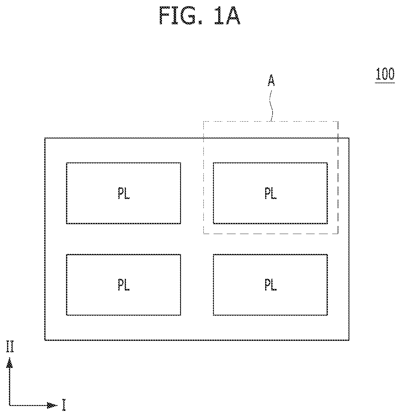
A and B are diagrams illustrating the structure of a semiconductor device in accordance with an embodiment. B illustrates section ‘A’ of A in accordance with an embodiment.
Referring to A and B , the semiconductor device may include at least one plane PL, a first peripheral circuit PR 1 , or a pad PAD, or a combination thereof. The semiconductor device may be a semiconductor chip 100 .
The planes PL may be arranged in a first direction I, in a second direction II intersecting the first direction I, or in the first direction I and the second direction II. The pad PAD and the first peripheral circuit PR 1 may be located around the planes PL. For example, the pad PAD and the first peripheral circuit PR 1 may be located in an edge area 100 _E of the semiconductor chip 100 . The pad PAD may include input/output terminals for receiving a signal from the outside or outputting a signal to the outside. The first peripheral circuit PR 1 may include circuits for operating the semiconductor chip 100 . The first peripheral circuit PR 1 may include a logic circuit, a data path, a read-only memory (ROM), or an analog circuit, or a combination thereof. For example, a read-only memory (ROM) area including the read-only memory (ROM) may be located in the edge area 100 _E of the semiconductor chip 100 , and the read-only memory (ROM) may be included in the logic circuit.
The plane PL may include a cell array CA or a second peripheral circuit PR 2 . The cell array CA may include stacked memory cells. For example, the cell array CA may include memory strings. Each of the memory strings may include at least one source select transistor, a plurality of memory cells, and at least one drain select transistor.
The second peripheral circuit PR 2 may be located inside the plane PL. The second peripheral circuit PR 2 may include a page buffer, a row decoder, or a read-only memory (ROM), or a combination thereof. The second peripheral circuit PR 2 may be stacked on or below the cell array CA. Alternatively, the second peripheral circuit PR 2 may be distributed around the cell array CA.
Referring to A and B , the first peripheral circuit PR 1 or the second peripheral circuit PR 2 may include the read-only memory (ROM). The read-only memory (ROM) area including the read-only memory (ROM) may be located in the edge area 100 _E of the semiconductor chip 100 or located inside the plane PL. The read-only memory (ROM) is a memory in which data written during a manufacturing process is stored, and may be a memory in which read is only possible and correction or erase of data is not possible. For example, reference data necessary for driving the semiconductor chip 100 may be stored in the read-only memory (ROM). For example, the reference data may include algorithm codes for programming, erasing, and reading the semiconductor chip 100 .
According to the structure described above, the read-only memory (ROM) area may be located in the edge area 100 _E of the semiconductor chip 100 or located inside the plane PL. Accordingly, in an embodiment, the read-only memory (ROM) may be efficiently disposed in the semiconductor chip 100 , and the degree of integration of the semiconductor device may be improved.
A and B are diagrams for describing the structure of a semiconductor device in accordance with an embodiment. A may be a plan view of the semiconductor device, and B may be a cross-sectional view of an edge area 23 _E of a source structure 23 . Hereinafter, the content overlapping with the previously described content will be omitted.
Referring to A and B , a semiconductor device 200 may include a substrate 20 , the source structure 23 , a stack 25 , or a read-only memory (ROM), or a combination thereof. The semiconductor device 200 may further include an isolation layer ISO, a spacer SP, an insulating spacer 26 , or an interlayer dielectric layer IL, or a combination thereof. The read-only memory (ROM) may be located in a read-only memory (ROM) area, and may include a transistor 21 or an interconnection structure IC, or a combination thereof. In an embodiment, a ROM area might include a first contact plug 24 located in the edge area 23 _E of the source structure 23 and a second contact plug 27 connected to the first contact plug 24 by extending through the stack 25 . In an embodiment, a ROM area might include a transistor 21 electrically connected to a first contact plug 24 . The semiconductor device may be a semiconductor chip 200 . In an embodiment, the ROM area is located in an edge area 23 _E of a semiconductor chip 200 .
The source structure 23 may be located on the substrate 20 . The source structure 23 may be located in a cell array CA and may extend up to a position where a first peripheral circuit PR 1 is formed. The source structure 23 may include a cell area 23 _C and the edge area 23 _E. A portion of the source structure 23 located in the cell array CA may be the cell area 23 _C, and a portion of the source structure 23 extending to the first peripheral circuit PR 1 may be the edge area 23 _E. The source structure 23 may include a conductive material such as polysilicon or metal.
The stack 25 may be located on the source structure 23 . For example, the stack 25 may be located on the edge area 23 _E of the source structure 23 . The stack 25 may include a first stack ST 1 , a second stack ST 2 , or a third stack ST 3 , or a combination thereof. The first stack ST 1 may be adjacent to the edge area 23 _E of the source structure 23 , and the second stack ST 2 may be spaced apart from the edge area 23 _E of the source structure 23 . The third stack ST 3 may be located on the second stack ST 2 . The first height H 1 of the first stack ST 1 may be substantially the same as or different from the second height H 2 of the second stack ST 2 . For example, the first height H 1 of the first stack ST 1 may be lower than the second height H 2 of the second stack ST 2 .
The stack 25 may include an insulating layer 25 A or a sacrificial layer 25 B. For example, the stack 25 may include insulating layers 25 A and sacrificial layers 25 B that are alternately stacked. The sacrificial layers 25 B may remain in the process of forming a gate structure of the cell array CA. The insulating layer 25 A may include an insulating material such as oxide, and the sacrificial layers 25 B may include a sacrificial material such as nitride. For reference, at least a part of the stack 25 may also include a conductive layer instead of the sacrificial layer 25 B.
The read-only memory (ROM) is a storage element for storing reference data and may include the transistor 21 , a fuse, and the like. For example, the transistor 21 may be located in an active area of the substrate 20 . The isolation layer ISO may be located in the substrate 20 , and the active area may be defined by the isolation layer ISO. The transistor 21 may include a first junction 21 A, a second junction 21 B, a gate insulating layer 21 C, or a gate electrode 21 D. The gate insulating layer 21 C may be located between the gate electrode 21 D and the substrate 20 . The gate insulating layer 21 C and the isolation layer ISO may include an insulating material such as oxide or nitride.
The read-only memory (ROM) may include the interconnection structure IC electrically connected to a storage element. For example, data stored in the transistor 21 may be output through the interconnection structure IC. Alternatively, the interconnection structure IC may also be used as a path for writing reference data to the read-only memory (ROM) during the manufacturing process.
The interconnection structure IC may include first contact plugs 24 , second contact plugs 27 , third contact plugs 22 A, or wirings 22 B, or a combination thereof.
The first contact plugs 24 may be located in the source structure 23 . For example, the first contact plugs 24 may be located in the edge area 23 _E of the source structure 23 . The first contact plugs 24 may pass through the edge area 23 _E of the source structure 23 . Each of the first contact plugs 24 may be connected to the wiring 22 B by extending through the source structure 23 . The spacer SP may be located on a sidewall of the first contact plug 24 , and the first contact plugs 24 and the source structure 23 may be insulated from each other by the spacer SP.
The second contact plugs 27 may be located on the edge area 23 _E of the source structure 23 . The second contact plugs 27 may pass through the stack 25 . The second contact plugs 27 may extend through the stack 25 in the stacking direction of the insulating layers 25 A. For example, the second contact plugs 27 may be respectively connected to the first contact plugs 24 by extending through the stack 25 . The second contact plugs 27 may be respectively connected to the first contact plugs 24 by passing through the stack 25 .
The insulating spacer 26 may be located in the stack 25 . The insulating spacer 26 may pass through a part of the stack 25 . For example, the insulating spacer 26 may pass through the first stack ST 1 . The insulating spacer 26 may surround a sidewall of the second contact plug 27 .
For reference, the film configuration and shape of the insulating spacer 26 may be changed. The insulating spacer 26 may be a single layer or a multilayer layer. The insulating spacer 26 may extend into the second stack ST 2 or into the third stack ST 3 while surrounding the sidewall of the contact plug 27 . Alternatively, the semiconductor device 200 might not include the insulating spacer 26 .
The third contact plugs 22 A or the wirings 22 B may be located below the source structure 23 . For example, the third contact plugs 22 A or the wirings 22 B may be located below the edge area 23 _E of the source structure 23 . The interlayer dielectric layer IL may be located between the substrate 20 and the source structure 23 , and the third contact plugs 22 A or the wirings 22 B may be located in the interlayer dielectric layer IL. Each of the third contact plugs 22 A may connect the junctions 21 A and 21 B of the transistor 21 to the wiring 22 B or may connect the wirings 22 B. The wirings 22 B may connect the third contact plugs 22 A, or may connect the first contact plug 24 and the third contact plug 22 A.
The first contact plugs 24 , the second contact plugs 27 , the third contact plugs 22 A or the wirings 22 B may each include a conductive material such as aluminum, copper, or tungsten. The spacer SP or the insulating spacer 26 may include an insulating material such as oxide, nitride, or air gap.
According to the structure described above, the read-only memory (ROM) may include the transistor 21 for storing data, and the interconnection structure IC for providing a path for inputting and outputting signals to and from the transistor 21 . The read-only memory (ROM) area may be located in the edge area 23 _E of the source structure 23 , and the read-only memory (ROM) may have a three-dimensional structure similar to that of the cell array CA.
A to C are diagrams for describing a semiconductor device in accordance with an embodiment. Hereinafter, the content overlapping with the previously described content will be omitted.
Referring to A , the semiconductor device may include a substrate 30 , a source structure 33 , a gate structure 35 D, a channel structure CH, or a source contact structure SC, or a combination thereof. The semiconductor device may further include a peripheral circuit PC, an interlayer dielectric layer IL, or an isolation insulating layer 38 , or a combination thereof.
The source structure 33 may be located on the substrate 30 . The source structure 33 may include a cell area and an edge area. A may be a cross-sectional view of the cell array CA described with reference to A , and may illustrate the cell area of the source structure 33 . For example, the cell area of the source structure 33 may be the cell area 23 _C of the source structure 23 in A . The source structure 33 illustrated in A and the source structure 23 in B may be interconnected.
The peripheral circuit PC may be located below the source structure 33 . The peripheral circuit PC may be the second peripheral circuit PR 2 in A , and may include a page buffer or a row decoder. The peripheral circuit PC may include a transistor having a structure similar to that of the transistor 21 in B . A peripheral circuit interconnection connected to the peripheral circuit PC may be included in the interlayer dielectric layer IL. The peripheral circuit interconnection may correspond to the third contact plugs 22 A or the wirings 22 B in B .
The gate structure 35 D may be located on the source structure 33 . For example, the gate structure 35 D may be located on the cell area of the source structure 33 . The gate structure 35 D may have a structure similar to that of the stack 25 in B . The gate structure 35 D may include insulating layers 35 A and conductive layers 35 C that are alternately stacked. The gate structure 35 D may be connected to the stack 25 in B . For example, the insulating layers 25 A of the stack 25 in B and the insulating layers 35 A of the gate structure 35 D may be an interconnected single layer. The sacrificial layers 25 B of the stack 25 in B may remain without being replaced with the conductive layers 35 C during a manufacturing process.
The gate structure 35 D may include a first gate structure GST 1 , a second gate structure GST 2 , or a third gate structure GST 3 , or a combination thereof. The first gate structure GST 1 may be adjacent to the cell area of the source structure 33 , and the second gate structure GST 2 may be spaced apart from the cell area of the source structure 33 . The third gate structure GST 3 may be located on the second gate structure GST 2 . The conductive layers 35 C of the first gate structure GST 1 may be source select lines, and the conductive layers 35 C of the second gate structure GST 2 may be word lines. At least one uppermost conductive layer 35 C of the third gate structure GST 3 may be a drain select line, and the remaining conductive layers 35 C may be word lines.
The first gate structure GST 1 may correspond to the first stack ST 1 in B , the second gate structure GST 2 may correspond to the second stack ST 2 in B , and the third gate structure GST 3 may correspond to the third stack ST 3 . The first height H 1 of the first gate structure GST 1 may be substantially the same as or different from the second height H 2 of the second gate structure GST 2 . For example, the first height H 1 of the first gate structure GST 1 may be lower than the second height H 2 of the second gate structure GST 2 . The insulating layer 35 A may include an insulating material such as oxide, and the conductive layers 35 C may include a conductive material such as polysilicon, tungsten, or molybdenum.
The isolation insulating layer 38 may be located in the gate structure 35 D. The isolation insulating layer 38 may pass through a part of the gate structure 35 D. For example, the isolation insulating layer 38 may pass through the first gate structure GST 1 . The isolation insulating layer 38 may be connected to the cell area of the source structure 33 by passing through the first gate structure GST 1 . The isolation insulating layer 38 may correspond to the insulating spacer 26 in B . For example, the isolation insulating layer 38 may be located at substantially the same level as the insulating spacer 26 in B or may include substantially the same material as the insulating spacer 26 in B . The isolation insulating layer 38 may electrically isolate source select lines located at substantially the same level. Consequently, the source select lines may be individually driven. The isolation insulating layer 38 may include an insulating material such as oxide or nitride.
The channel structures CH may be located on the source structure 33 . For example, the channel structures CH may be located on the cell area of the source structure 33 . Each of the channel structures CH may pass through the gate structure 35 D. Each of the channel structures CH may extend in a direction, in which the insulating layers 35 A are stacked, through the gate structure 35 D and may be connected to the cell area of the source structure 33 . For example, a channel layer CHa may be directly connected to the source structure 33 , or may be connected to the cell area of the source structure 33 through an epitaxially grown semiconductor pattern.
Each of the channel structures CH may further include at least one of a memory layer CHb surrounding a sidewall of the channel layer CHa and an insulating core CHc in the channel layer CHa. The channel layer CHa may include a semiconductor material such as silicon or germanium. The memory layer CHb may include a blocking layer, a data storage layer, or a tunneling layer, or a combination thereof. The insulating core CHc may include an insulating material such as oxide, nitride, or an air gap.
The source contact structure SC may be located on the source structure 33 . For example, the source contact structure SC may be located on the cell area of the source structure 33 . The source contact structure SC may pass through the gate structure 35 D. The source contact structure SC may extend in a direction, in which the insulating layers 35 A are stacked, through the gate structure 35 D and may be connected to the cell area of the source structure 33 .
The source contact structure SC may include a source contact plug SCa or a source contact spacer SCb. The source contact plug SCa may extend in the stacking direction of the insulating layers 35 A through the gate structure 35 D and may be connected to the cell area of the source structure 33 . The source contact spacer SCb may surround a sidewall of the source contact plug SCa. The source contact plug SCa may include polysilicon, metal, or the like. The source contact spacer SCb may include an insulating material such as oxide, nitride, or an air gap.
Referring to B , the semiconductor device may further include a contact structure CT, a spacer SP, a dummy stack 35 , or a first cell contact plug 34 , or a combination thereof.
The contact structure CT may be located in the source structure 33 . For example, the contact structure CT may be located in the cell area of the source structure 33 . The contact structure CT may pass through the source structure 33 . For example, the contact structure CT may pass through the cell area of the source structure 33 . The spacer SP may surround a sidewall of the contact structure CT. The contact structure CT may have a structure similar to that of the first contact plugs 24 in B . For example, the contact structure CT may be located at substantially the same level as the first contact plugs 24 in B or may include substantially the same material as the first contact plugs 24 in B . The contact structure CT may include a conductive material such as tungsten, and the spacer SP may include an insulating material such as oxide.
The dummy stack 35 may be located on the source structure 33 . For example, the dummy stack 35 may be located on the cell area of the source structure 33 . The dummy stack 35 may have a structure similar to that of the stack 25 in B . The dummy stack 35 may include insulating layers 35 A and sacrificial layers 35 B that are alternately stacked. The dummy stack 35 may be connected to the stack 25 in B or the gate structure 35 D in A . For example, the insulating layers 25 A of the stack 25 in B , and the insulating layers 35 A of the gate structure 35 D may be an interconnected single layer. The insulating layer 35 A may include an insulating material such as oxide, and the sacrificial layer 35 B may include a sacrificial material such as nitride.
The first cell contact plug 34 may be located on the contact structure CT. The first cell contact plug 34 may pass through the dummy stack 35 . The first cell contact plug 34 may extend in the stacking direction of the insulating layers 35 A through the dummy stack 35 . The first cell contact plug 34 may be connected to the contact structure CT by passing through the dummy stack 35 . The first cell contact plug 34 may have a structure similar to that of the second contact plug 27 in B . For example, the first cell contact plug 34 may be located at substantially the same level as the second contact plug 27 in B . The first cell contact plug 34 may be a part of an interconnection structure electrically connected to the peripheral circuit PC together with the contact structure CT or may be a support used in a manufacturing process. The first cell contact plug 34 may include a conductive material such as tungsten or an insulating material such as oxide.
Referring to C , the semiconductor device may further include second cell contact plugs 37 .
The gate structure 35 D may have a stepped structure SR. The stepped structure SR may include insulating layers 35 A and conductive layers 35 C that are alternately stacked. The gate structure 35 D may include at least one stepped structure SR so that the conductive layers 35 C are exposed. For example, the stepped structure SR may include a first stepped structure SR 1 , a second stepped structure SR 2 , a third stepped structure SR 3 , and a fourth stepped structure SR 4 .
The second cell contact plugs 37 may pass through the interlayer dielectric layer IL, the gate structure 35 D, and the source structure 33 . Each of the second cell contact plugs 37 may be electrically connected to the conductive layer 35 C exposed on the top of each of the stepped structures SR 1 to SR 4 . For example, each of the second cell contact plugs 37 may include a protrusion on a sidewall thereof, and may be electrically connected to the conductive layer 35 C, which is exposed on the top of each of the stepped structures SR 1 to SR 4 , by the protrusion. A cell spacer CSP may be located on a part of the sidewall of each of the second cell contact plugs 37 . The cell spacer CSP may be located between the second cell contact plugs 37 and the conductive layers 35 C. The cell spacer CSP may insulate the second cell contact plug 37 from the remaining conductive layers 35 C except for the uppermost conductive layer 35 C of each of the stepped structures SR 1 to SR 4 .
The second cell contact plug 37 may have a structure similar to that of the second contact plug 27 in B . For example, the second cell contact plug 37 may be located at substantially the same level as the second contact plug 27 in B or may include substantially the same material as the second contact plug 27 in B . The second cell contact plugs 37 may each include a conductive material such as tungsten. The cell spacer CSP may include an insulating material such as oxide, nitride, or an air gap.
For reference, although not illustrated in the drawing, the second cell contact plugs 37 may be connected to the peripheral circuit PC located below the source structure 33 by passing through the source structure 33 . C illustrates that the second cell contact plugs 37 pass through the interlayer dielectric layer IL, the gate structure 35 D, and the source structure 33 ; however, the present disclosure is not limited thereto. For example, each of the second cell contact plugs 37 may be connected to the conductive layer 35 C exposed on the top of each of the stepped structures SR 1 to SR 4 by passing through the interlayer dielectric layer IL. In this case, the second cell contact plugs 37 may each include no protrusion.
According to the structure described above, structures constituting a cell array may correspond to structures constituting a read-only memory (ROM). Accordingly, the read-only memory (ROM) having a three-dimensional structure similar to that of the cell array may be implemented.
A to F are diagrams for describing a method of manufacturing a semiconductor device in accordance with an embodiment. Hereinafter, the content overlapping with the previously described content will be omitted.
Referring to A , a storage element of a read-only memory (ROM) may be formed on a substrate 40 . For example, a transistor 41 , which is the storage element of the read-only memory (ROM), may be formed in a read-only memory (ROM) area. An isolation layer ISO may be formed in the substrate 40 , and a gate insulating layer 41 C, a gate electrode 41 D, and junctions 41 A and 41 B may be formed. For reference, a storage element such as a fuse may also be formed instead of the transistor 41 .
Subsequently, third contact plugs 42 A and wirings 42 B connected to the transistor 41 may be formed. The third contact plugs 42 A and the wirings 42 B may be formed in the interlayer dielectric layer IL.
Subsequently, a source structure 43 may be formed. The source structure 43 may include a cell area and an edge area. For example, the edge area of the source structure 43 may be the edge area 23 _E of the source structure 23 in A , and may correspond to the edge area of the semiconductor chip 200 .
Subsequently, first contact plugs 44 passing through the source structure 43 may be formed. First, openings, which expose the third contact plugs 42 A or the wirings 42 B by passing through the edge area of the source structure 43 , may be formed, and insulating layers may be formed in the openings, respectively. Subsequently, the first contact plugs 44 may be formed in the insulating layers, respectively. In this case, insulating layers remaining while forming the first contact plugs 44 may be defined as spacers SP. The first contact plugs 44 may be used as a path for outputting data stored in the transistor 41 or writing data.
Referring to B , a first stack ST 1 may be formed on the source structure 43 . For example, the first stack ST 1 may be formed on the edge area of the source structure 43 . For reference, the first stack ST 1 may extend up to the cell area of the source structure 43 . The first stack ST 1 may be formed by alternately stacking first material layers 45 A and second material layers 45 B. For example, the first material layers 45 A may each include an insulating material such as oxide, and the second material layers 45 B may each include a sacrificial material such as nitride or a conductive material such as polysilicon, tungsten, and molybdenum.
Subsequently, first sacrificial layers 46 A may be formed. First, a first opening OP 1 , which exposes each of the first contact plugs 44 , may be formed by passing through the first stack ST 1 . Subsequently, the first sacrificial layer 46 A may be formed in the first opening OP 1 . Each of the first sacrificial layers 46 A may be connected to the first contact plug 44 by passing through the first stack ST 1 . When the first sacrificial layer 46 A is formed, an isolation insulating layer of a cell array may be formed together. This will be described below with reference to A to C .
Referring to C , a second stack ST 2 may be formed on the first stack ST 1 . Subsequently, a third stack ST 3 may be formed on the second stack ST 2 . Accordingly, a stack 45 including the first stack ST 1 , the second stack ST 2 , and the third stack ST 3 may be formed. The second stack ST 2 and the third stack ST 3 may each be formed by alternately stacking the first material layers 45 A and the second material layers 45 B. The first height H 1 of the first stack ST 1 may be substantially the same as or different from the second height H 2 of the second stack ST 2 . For example, the first height H 1 of the first stack ST 1 may be formed to be lower than the second height H 2 of the second stack ST 2 .
Subsequently, a second opening OP 2 may be formed to expose each of the first sacrificial layers 46 A by passing through the second stack ST 2 and the third stack ST 3 . In this case, a part of an upper surface of each of the first sacrificial layers 46 A may be etched. When the second opening OP 2 is formed, a fifth opening OP 5 of the cell array may be formed together. This will be described below with reference to .
Referring to D , second sacrificial layers 46 B may be formed. Each of the second sacrificial layers 46 B may be formed in the second opening OP 2 . Each of the second sacrificial layers 46 B may be connected to the first sacrificial layers 46 A by passing through the third stack ST 3 and the second stack ST 2 . The second sacrificial layers 46 B may each include substantially the same material as the first sacrificial layers 46 A. The second sacrificial layers 46 B may each include an insulating material such as oxide or nitride.
For reference, in the present embodiment, a case in which the second opening OP 2 passing through the second stack ST 2 and the third stack ST 3 is formed at once has been described; however, the second opening OP 2 passing through the second stack ST 2 and a third opening passing through the third stack ST 3 may be formed. For example, a second opening, which exposes the first sacrificial layers 46 A, may be formed by passing through the second stack ST 2 , and a second sacrificial layer may be formed in the second opening. Subsequently, a third opening passing through the third stack ST 3 may be formed, and third sacrificial layers may be formed in the third opening.
Referring to E , third openings OP 3 passing through the stack 45 may be formed. The first opening OP 1 and the second opening OP 2 may be re-opened by etching the second sacrificial layer 46 B and the first sacrificial layer 46 A. For example, the second opening OP 2 and the first opening OP 1 may be formed by etching the second sacrificial layer 46 B and the first sacrificial layer 46 A by using a mask pattern as an etch barrier. Alternatively, the second sacrificial layer 46 B and the first sacrificial layer 46 A may be selectively etched under conditions having an etch selectivity with respect to the first material layers 45 A and the second material layers 45 B. In this case, the first opening OP 1 and the second opening OP 2 connected to each other may be defined as the third opening OP 3 . Each of the third openings OP 3 may pass through the third stack ST 3 , the second stack ST 2 , and the first stack ST 1 . Each of the third openings OP 3 may expose the first contact plug 44 . When the third opening OP 3 is formed, a sixth opening OP 6 of the cell array may be formed together. This will be described below with reference to .
When the third openings OP 3 are formed, a part of the second sacrificial layer 46 B or the first sacrificial layer 46 A may remain without being etched. For example, in the process of etching the first sacrificial layer 46 A, a part of the first sacrificial layer 46 A may remain in the first opening OP 1 , and the remaining portion may be used as an insulating spacer 46 . For reference, a part of the second sacrificial layer 46 B may remain, or both the second sacrificial layer 46 B and the first sacrificial layer 46 A may be removed.
Referring to F , second contact plugs 47 may be formed. The second contact plug 47 may be formed in the third openings OP 3 , respectively. The second contact plugs 47 may be formed to be respectively connected to the first contact plugs 44 . The second contact plugs 47 may be used as a path for outputting data stored in the transistor 41 or writing data. When the second contact plugs 47 are formed, second cell contact plugs 77 of the cell array may be formed together. This will be described below with reference to .
For reference, an insulating spacer may be additionally formed in the third opening OP 3 before the second contact plugs 47 are formed. For example, after the insulating spacer is formed on sidewalls of the first stack ST 1 , the second stack ST 2 , and the third stack ST 3 exposed through the third openings OP 3 , the second contact plugs 47 may also be formed.
Furthermore, when the second material layers 44 B are sacrificial layers, the second material layers 44 B may be substantially maintained as they are or replaced with third material layers each including a conductive layer during the manufacturing process. When the second material layers 44 B are replaced with the conductive layers, an insulating spacer may be additionally formed before the second contact plugs 47 are formed, so that the second contact plug 47 and the third material layers may be electrically separated from each other.
Accordingly, an interconnection structure IC including the first contact plugs 44 , the second contact plugs 47 , the third contact plugs 42 A or the wirings 42 B, or a combination thereof may be formed. Furthermore, a read-only memory (ROM) including the interconnection structure (IC) and the transistor 41 may be formed in the read-only memory (ROM) area.
Subsequently, reference data may be written to the read-only memory (ROM). For example, reference data may be written by applying a bias to the transistor 41 through the interconnection structure IC. For reference, in the present embodiment, a case in which data is written to the read-only memory (ROM) after both the storage element and the interconnection structure are formed has been described; however, the source structure, the interconnection structure, and the like may be formed after data is written to a fuse and the like.
According to the manufacturing method described above, in forming the second contact plug 47 having a large aspect ratio, the third opening OP 3 may be formed through a plurality of processes. After the first opening OP 1 passing through the first stack ST 1 is formed first, the second opening OP 2 passing through the second stack ST 2 and the third stack ST 3 may be formed.
When the third opening OP 3 having a large aspect ratio is etched in a one-time etching process, the third opening OP 3 may be formed to have a non-uniform depth or a not-open phenomenon may occur in which the third opening OP 3 is not etched to a desired depth. In the case of the edge area of the source structure 43 , this phenomenon may occur more frequently due to limitations in the etching process. Therefore, this phenomenon may be minimized or substantially prevented by forming the third opening OP 3 located in the edge area of the source structure 43 through a plurality of processes. Furthermore, a read-only memory (ROM) having a three-dimensional structure may be formed in the read-only memory (ROM) area by using a cell array process.
A to C are diagrams for describing a method of manufacturing a semiconductor device in accordance with an embodiment. Hereinafter, the content overlapping with the previously described content will be omitted.
Referring to A , a source structure 53 may be formed. Although not illustrated in A , a peripheral circuit and a peripheral circuit interconnection connected to the peripheral circuit may be formed before the source structure 53 is formed. For example, when forming the transistor 41 , the third contact plugs 42 A, or the wirings 42 B in A , the peripheral circuit and the peripheral circuit interconnection may be formed. The source structure 53 may include a cell area and an edge area. The cell area of the source structure 53 may be the cell area 23 _C of the source structure 23 in A , and may correspond to the cell area of the semiconductor chip 200 .
Subsequently, a first stack ST 1 may be formed on the source structure 53 . For example, the first stack ST 1 may be formed on the cell area of the source structure 53 . The first stack ST 1 may be formed by alternately stacking first material layers 55 A and second material layers 55 B. For reference, the first stack ST 1 may also extend up to the edge area of the source structure 53 . The first stack ST 1 may extend to be connected to the first stack ST 1 in B . For example, the first material layers 55 A of the first stack ST 1 may be connected to the first material layers 45 A of the first stack ST 1 in B , and the second material layers 55 B of the first stack ST 1 may be connected to the second material layers 45 B of the first stack ST 1 in B .
Subsequently, isolation insulating layers 58 passing through the first stack ST 1 may be formed. For example, the isolation insulating layers 58 passing through the first stack ST 1 and connected to the cell area of the source structure 53 may be formed. First, fourth openings OP 4 passing through the first stack ST 1 and exposing the cell area of the source structure 53 may be formed. Subsequently, the isolation insulating layers 58 may be formed in the fourth openings OP 4 , respectively.
When the isolation insulating layers 58 are formed, the first sacrificial layers 46 A in B may be formed. For example, the fourth openings OP 4 may be formed in the cell area of the source structure 53 by using substantially the same mask pattern as an etch barrier, and simultaneously the first openings OP 1 may be formed in the edge area of the source structure 43 . Furthermore, when the isolation insulating layers 58 are formed in the fourth openings OP 4 , respectively, the first sacrificial layers 46 A may be formed in the first openings OP 1 , respectively. Accordingly, the isolation insulating layer 58 may be formed to have a structure similar to that of the first sacrificial layer 46 A, and may be formed at substantially the same level as that of the first sacrificial layer 46 A or may include substantially the same material as that of the first sacrificial layer 46 A. The isolation insulating layers 58 may each include an insulating material such as oxide or nitride. The words “simultaneous” and “simultaneously” as used herein with respect to processes mean that the processes take place on overlapping intervals of time. For example, if a first process takes place over a first interval of time and a second process takes place simultaneously over a second interval of time, then the first and second intervals at least partially overlap each other such that there exists a time at which the first and second processes are both taking place.
Referring to B , a second stack ST 2 may be formed on the first stack ST 1 . The second stack ST 2 may be formed by alternately stacking the first material layers 55 A and the second material layers 55 B. The second stack ST 2 may extend to be connected to the second stack ST 2 in C . For example, the first material layers 55 A of the second stack ST 2 may be connected to the first material layers 45 A of the second stack ST 2 in C , and the second material layers 55 B of the second stack ST 2 may be connected to the second material layers 45 B of the second stack ST 2 in C . In this case, the first height H 1 of the first stack ST 1 may be lower than the second height H 2 of the second stack ST 2 .
Subsequently, first channel structures CH_ 1 passing through a part of the second stack ST 2 , the first stack ST 1 , and the source structure 53 may be formed. For example, the first channel structures CH_ 1 passing through a part of the second stack ST 2 , the first stack ST 1 , and the cell area of the source structure 53 may be formed. Each of the first channel structures CH_ 1 may further include at least one of a memory layer CHb_ 1 surrounding a sidewall of a channel layer CHa_ 1 or an insulating core CHc_ 1 in the channel layer CHa_ 1 .
Referring to C , a third stack ST 3 may be formed on the second stack ST 2 . The third stack ST 3 may be formed by alternately stacking the first material layers 55 A and the second material layers (not illustrated). The third stack ST 3 may extend to be connected to the third stack ST 3 in C . For example, the first material layers 55 A of the third stack ST 3 may be connected to the first material layers 45 A of the third stack ST 3 in C , and the second material layers 55 B of the third stack ST 3 may be connected to the second material layers 45 B of the third stack ST 3 in C .
Subsequently, channel structures CH passing through the third stack ST 3 may be formed. The channel structures CH may be formed by forming an opening, which exposes each of the first channel structures CH_ 1 by passing through the third stack ST 3 , and forming a second channel structure (not illustrated) in the opening. The channel structures CH may each include a channel layer CHa, a memory layer CHb, or an insulating core CHc, or a combination thereof.
Subsequently, a source contact structure SC passing through a part of the third stack ST 3 , the second stack ST 2 , the first stack ST 1 , and the source structure 53 may be formed. First, an opening passing through a part of the third stack ST 3 , the second stack ST 2 , the first stack ST 1 and the source structure 53 may be formed, and a source contact spacer SCb and a source contact plug SCa may be sequentially formed in the opening.
Before the source contact structure SC is formed, the first stack ST 1 , the second stack ST 2 , and the third stack ST 3 may be replaced with a first gate structure GST 1 , a second gate structure GST 2 , and a third gate structure GST 3 , respectively. For example, the second material layers 55 B of the first stack ST 1 , the second stack ST 2 , and the third stack ST 3 may be replaced with third material layers 55 C. In this case, the third material layer 55 C may be a conductive layer. Accordingly, a gate structure 55 including the first gate structure GST 1 , the second gate structure GST 2 , and the third gate structure GST 3 may be formed. The conductive layer may include a conductive material such as polysilicon, tungsten, or molybdenum.
According to the process described above, when the isolation insulating layers 58 are formed in the cell area of the source structure 53 , the first sacrificial layers 46 A may be formed in the edge area of the source structure 43 in B . Accordingly, a read-only memory (ROM) may be formed in a read-only memory (ROM) area of the edge area by utilizing the process performed in the cell area.
is a diagram for describing a method of manufacturing a semiconductor device in accordance with an embodiment. Hereinafter, the content overlapping with the previously described content will be omitted.
Referring to , a source structure 63 may be formed. Although not illustrated in , a peripheral circuit may be formed before the source structure 63 is formed. The source structure 63 may include a cell area and an edge area. The cell area of the source structure 63 may be the cell area 23 _C of the source structure 23 in A , and may correspond to the cell area of the semiconductor chip 200 .
Subsequently, a contact structure CT passing through the source structure 63 may be formed. First, an opening passing through the cell area of the source structure 63 may be formed, and an insulating layer may be formed in the opening. Subsequently, the contact structure CT may be formed in the insulating layer. In this case, an insulating layer remaining while forming the contact structure CT may be defined as a spacer SP. When the contact structure CT is formed, the first contact plugs 44 in A may be formed. For example, the first contact plugs 44 may be formed in the edge area of the source structure 43 by using, as an etch barrier, a mask pattern used when forming the contact structure CT in the cell area of the source structure 63 . Accordingly, the contact structure CT may be formed to have a structure similar to that of the first contact plug 44 , and may be formed at substantially the same level as that of the first contact plug 44 or may include substantially the same material as that of the first contact plug 44 . The contact structure CT may include a conductive material such as tungsten.
Subsequently, a dummy stack 65 may be formed on the source structure 63 . For example, the dummy stack 65 may be formed on the cell area of the source structure 63 . The dummy stack 65 may be formed by alternately stacking first material layers 65 A and second material layers 65 B. For reference, the dummy stack 65 may also extend up to the edge area of the source structure 63 . The dummy stack 65 may extend to be connected to the stack 45 in C . For example, the first material layers 65 A of the dummy stack 65 may be connected to the first material layers 45 A of the stack 45 in C , and the second material layers 65 B of the dummy stack 65 may be connected to the second material layers 45 B of the stack 45 in C .
Subsequently, a first cell contact plug 64 passing through the dummy stack 65 may be formed. For example, the first cell contact plug 64 passing through the dummy stack 65 and connected to the cell area of the source structure 63 may be formed. First, a fifth opening OP 5 , which exposes the cell area of the source structure 63 by passing through the dummy stack 65 , may be formed. Subsequently, the first cell contact plug 64 may be formed in the fifth opening OP 5 .
When the first cell contact plug 64 is formed, the second sacrificial layers 46 B in D may be formed. For example, the fifth opening OP 5 may be formed in the cell area of the source structure 63 by using substantially the same mask pattern as an etch barrier, and simultaneously the second openings OP 2 may be formed in the edge area of the source structure 43 . Furthermore, when the first cell contact plug 64 is formed in the fifth opening OP 5 , the second sacrificial layers 46 B may be formed in the second openings OP 2 , respectively. Accordingly, the first cell contact plug 64 may be formed to have a structure similar to that of the second sacrificial layer 46 B, and may be formed at substantially the same level as that of the second sacrificial layer 46 B or may include a material substantially the same as or different from that of the second sacrificial layer 46 B. The first cell contact plug 64 may include a conductive material such as tungsten, or an insulating material such as oxide or nitride.
For example, the first cell contact plug 64 may include an insulating material such as oxide or nitride. In such a case, the dummy stack 65 may be used as a support for minimizing the inclination of the dummy stack 65 in the process of replacing the dummy stack 65 with a gate structure. As another example, when a sacrificial layer is formed in the fifth opening OP 5 , the second sacrificial layers 46 B may be formed in the second openings OP 2 , respectively. Subsequently, the sacrificial layer in the fifth opening OP 5 may be replaced with a conductive material such as tungsten. Accordingly, the first cell contact plug 64 electrically connected to the contact structure CT may be formed, and may be electrically connected to a peripheral circuit.
According to the process described above, when the first cell contact plug 64 is formed in the cell area of the source structure 63 , the second sacrificial layers 46 B may be formed in the edge area of the source structure 43 in D . Accordingly, a read-only memory (ROM) may be formed in a read-only memory (ROM) area of the edge area by utilizing the process performed in the cell area.
is a diagram for describing a method of manufacturing a semiconductor device according to an embodiment. Hereinafter, the content overlapping with the previously described content will be omitted.
Referring to , a source structure 73 may be formed. Although not illustrated in , a peripheral circuit may be formed before forming the source structure 73 . The source structure 73 may include a cell area and an edge area. The cell area of the source structure 73 may be the cell area 23 _C of the source structure 23 in A , and may correspond to the cell area of the semiconductor chip 200 .
Subsequently, a stack 75 may be formed on the source structure 73 . For example, the stack 75 may be formed on the cell area of the source structure 73 . The stack 75 may be formed by alternately stacking first material layers 75 A and second material layers 75 B. For reference, the stack 75 may also extend up to the edge area of the source structure 73 . The stack 75 may extend to be connected to the stack 45 in C .
Subsequently, a channel structure CH passing through the stack 75 and a part of the source structure 73 may be formed. For example, the channel structure CH passing through the stack 75 and a part of the cell area of the source structure 73 may be formed. The channel structure CH may further include at least one of a memory layer CHb surrounding a sidewall of the channel layer CHa or an insulating core CHc within the channel layer CHa.
Subsequently, the stepped structure SR may be formed in the stack 75 . The stepped structure SR may include the first material layers 75 A and the second material layers 75 B alternately stacked. The stepped structure SR may include a first stepped structure SR 1 , a second stepped structure SR 2 , a third stepped structure SR 3 , and a fourth stepped structure SR 4 . A buffer layer may be formed on the uppermost second material layer 75 B exposed to each of the stepped structures SR 1 to SR 4 . The buffer layer is a sacrificial layer and used to form a protrusion of a second cell contact plug 77 to be described below. The buffer layer may be a single layer or a multilayer layer. Subsequently, an interlayer dielectric layer IL may be formed on the stack 75 . Subsequently, the second material layers 75 B may be replaced with third material layers 75 C. The third material layer 75 C may be a conductive layer, and may include a conductive material such as polysilicon, tungsten, or molybdenum. Accordingly, a gate structure 75 D including the first material layers 75 A and the third material layers 75 C alternately stacked may be formed.
Subsequently, the second cell contact plugs 77 connected to the stepped structure SR may be formed. First, the sixth openings OP 6 passing through the interlayer dielectric layer IL, the stepped structures SR 1 to SR 4 , and the source structure 73 may be formed. Subsequently, after openings are formed by selectively etching the second material layers 75 B, cell spacers CSP may be formed in the openings, respectively. Subsequently, after the buffer layers are removed, the second cell contact plugs 77 may be formed in the sixth openings OP 6 , respectively. The protrusions may be formed in the area from which the buffer layers are removed, and each of the second cell contact plugs 77 may be electrically connected to the uppermost conductive layer of each of the stepped structures SR 1 to SR 4 by the protrusion.
When the second cell contact plugs 77 are formed, the second contact plugs 47 in F may be formed. For example, the sixth openings OP 6 may be formed in the cell area of the source structure 73 by using substantially the same mask pattern as an etch barrier, and simultaneously the third openings OP 3 may be formed in the edge area of the source structure 43 . Furthermore, when the second cell contact plugs 77 are formed in the sixth openings OP 6 , respectively, the second contact plugs 47 may be formed in the third openings OP 3 , respectively.
Accordingly, the second cell contact plug 77 may be formed to have a structure similar to that of the second contact plug 47 , and may be formed at substantially the same level as of the second contact plug 47 or may include substantially the same material as of the second contact plug 47 . The second cell contact plug 77 may include a conductive material such as tungsten.
For reference, although not illustrated in , the second cell contact plugs 77 may be connected to a peripheral circuit formed below the source structure 73 by passing through the source structure 73 .
According to the process described above, when the second cell contact plugs 77 are formed in the cell area of the source structure 73 , the second contact plugs 47 may be formed in the edge area of the source structure 43 in F . Accordingly, in an embodiment, a read-only memory (ROM) may be formed in a read-only memory (ROM) area of the edge area by utilizing the process performed in the cell area.
Although embodiments according to the technical idea of the present disclosure have been described above with reference to the accompanying drawings, this is only for explaining the embodiments according to the concept of the present disclosure, and the present disclosure is not limited to the above embodiments. Various types of substitutions, modifications, and changes for the embodiments may be made by those skilled in the art, to which the present disclosure pertains, without departing from the technical idea of the present disclosure defined in the following claims, and it should be construed that these substitutions, modifications, and changes belong to the scope of the present disclosure.
Figures (18)
Citations
This patent cites (4)
- US2019/0081017
- US2021/0313343
- US1020210121335
- US1020210124836