LED Current Overshoot Reduction Apparatus and Method
Abstract
An apparatus includes a reference current generation circuit coupled between a first voltage bus and a second voltage bus, wherein the reference current generation circuit is configured to generate a predetermined reference current, a first reference current path comprising a first switch, wherein the predetermined reference current is configured to be mirrored to generate a first reference current in the first reference current path, a load current path comprising a power switch, and a pulse width modulation (PWM) deglitch circuit configured to control the first switch so as to reduce an overshoot occurring at a leading-edge of a load current flowing through the power switch.
Claims (20)
1 . An apparatus comprising: a reference current generation circuit coupled between a first voltage bus and a second voltage bus, wherein the reference current generation circuit is configured to generate a predetermined reference current; a first reference current path comprising a first switch, wherein the predetermined reference current is configured to be mirrored to generate a first reference current in the first reference current path; a load current path comprising a power switch; and a pulse width modulation (PWM) deglitch circuit configured to control the first switch so as to reduce an overshoot occurring at a leading-edge of a load current flowing through the power switch.
12 . A method comprising: generating a predetermined reference current using a reference current generation circuit coupled between a first voltage bus and a second voltage bus; mirroring the predetermined reference current to generate a first reference current in a first reference current path comprising a first switch; and controlling, by a PWM deglitch circuit, the first switch to reduce an overshoot occurring at a leading-edge of a load current flowing through a power switch.
17 . A system comprising: a PWM switch, an integrated circuit and a light-emitting diode connected in series between a power source and ground; and a system controller configured to control the PWM switch, wherein the integrated circuit comprises: a low-dropout regulator having an input configured to receive an input voltage and an output configured to generate a bias voltage on a first voltage bus; an undervoltage lockout circuit configured to receive the bias voltage and generate a control signal applied to a gate of a power switch, wherein a current flowing through the power switch is approximately equal to a current flowing through the light-emitting diode; a bandgap reference circuit configured to receive the bias voltage and generate a bandgap reference; a reference current generation circuit coupled between the first voltage bus and a second voltage bus, wherein the reference current generation circuit is configured to generate a predetermined reference current; a first reference current path comprising a first switch, wherein the predetermined reference current is configured to be mirrored to generate a first reference current in the first reference current path; and a PWM deglitch circuit configured to control the first switch so as to reduce an overshoot occurring at a leading-edge of a load current flowing through the power switch.
Show 17 dependent claims
2 . The apparatus of claim 1 , wherein: the first reference current is mirrored to generate the load current flowing through the power switch.
3 . The apparatus of claim 1 , further comprising: a second reference current path connected in parallel with the first reference current path, wherein: the second reference current path comprises a third p-type transistor; the predetermined reference current is configured to be mirrored to generate a second reference current in the second reference current path; and a sum of the first reference current and the second reference current is mirrored to generate the load current flowing through the power switch.
4 . The apparatus of claim 1 , further comprising: a second reference current path connected in parallel with the first reference current path; a third reference current path connected in parallel with the first reference current path, wherein the third reference current path comprises a fourth p-type transistor and a second switch connected in series, and wherein the second switch is controlled by the PWM deglitch circuit; and a fourth reference current path connected in parallel with the first reference current path, wherein the fourth reference current path comprises a fifth p-type transistor and a third switch connected in series, and wherein the third switch is controlled by the PWM deglitch circuit, wherein: the predetermined reference current is configured to be mirrored to generate a second reference current in the second reference current path; the predetermined reference current is configured to be mirrored to generate a third reference current in the third reference current path; the predetermined reference current is configured to be mirrored to generate a fourth reference current in the fourth reference current path; and a sum of the first reference current, the second reference current, the third reference current and the fourth reference current is mirrored to generate the load current flowing through the power switch.
5 . The apparatus of claim 4 , wherein the PWM deglitch circuit comprises: a first inverter configured to receive a reference voltage signal proportional to the predetermined reference current; a second inverter having an input connected to an output of the first inverter and an output configured to generate a first control signal applied to a gate of the first switch; a leading-edge blanking circuit having an input configured to receive the first control signal, and an output configured to generate a third control signal applied to a gate of the third switch; and an XOR gate, an inverter and an NOR gate connected in cascade, wherein: a first input of the XOR gate is configured to receive the first control signal; a second input of the XOR gate is configured to receive the third control signal; an input of the inverter is connected to an output of the XOR gate; a first input of the NOR gate is configured to receive the third control signal; a second input of the NOR gate is connected to an output of the inverter; and an output of the NOR gate is configured to generate a second control signal applied to a gate of the second switch.
6 . The apparatus of claim 1 , wherein: the reference current generation circuit comprises: a first p-type transistor and a resistor connected in series between the first voltage bus and the second voltage bus; and a first amplifier having an inverting input configured to receive a bandgap reference, a non-inverting input connected to a common node of the first p-type transistor and the resistor, and an output connected to a gate of the first p-type transistor and a gate of a second p-type transistor; and the first reference current path comprises the second p-type transistor and the first switch connected in series, and wherein the first p-type transistor and the second p-type transistor form a first current mirror through which the predetermined reference current is mirrored to generate the first reference current in the first reference current path.
7 . The apparatus of claim 6 , further comprising: a first n-type transistor connected in series with the first reference current path; a second n-type transistor connected in series with the power switch, wherein the first n-type transistor and the second n-type transistor form a second current mirror through which the first reference current is mirrored to generate the load current flowing through the power switch; and a second amplifier having an inverting input connected to a drain of the first n-type transistor, a non-inverting input connected to a drain of the second n-type transistor, and an output connected to a gate of the first n-type transistor and a gate of the second n-type transistor.
8 . The apparatus of claim 7 , further comprising: a reference current subtraction circuit configured to reduce the first reference current so as to reduce the overshoot occurring at the leading-edge of the load current, wherein the reference current subtraction circuit comprises: a first current subtraction transistor connected between the drain of the first n-type transistor and the second voltage bus; a rise detection capacitor and a rise detection resistor connected in series between the common node of the first p-type transistor and the resistor, and the second voltage bus, and wherein a common node of the rise detection capacitor and the rise detection resistor is connected to a gate of the first current subtraction transistor; a second current subtraction transistor connected between the drain of the first n-type transistor and the second voltage bus; and a fall detection resistor and a fall detection capacitor connected in series between the common node of the first p-type transistor and the resistor, and the second voltage bus, and wherein a common node of the fall detection resistor and the fall detection capacitor is connected to a gate of the second current subtraction transistor.
9 . The apparatus of claim 1 , further comprising: a low-dropout regulator having an input configured to receive an input voltage and an output configured to generate a bias voltage; an undervoltage lockout circuit configured to receive the bias voltage and generate a control signal applied to a gate of the power switch; and a bandgap reference circuit configured to receive a bias voltage from a bias power supply and generate a bandgap reference.
10 . The apparatus of claim 1 , further comprising: a gate protection circuit connected between a gate of the power switch and the second voltage bus, wherein the gate protection circuit comprises a first resistor, a second resistor, a capacitor and a third n-type transistor, and wherein: the third n-type transistor is connected between the gate of the power switch and the second voltage bus; the capacitor and the first resistor are connected in series between the gate of the power switch and the second voltage bus; and the second resistor is connected between the gate of the power switch and the second voltage bus.
11 . The apparatus of claim 1 , further comprising: a startup circuit comprising a third current mirror comprising a fourth n-type transistor and a fifth n-type transistor and a sixth p-type transistor, and wherein: the sixth p-type transistor and the fifth n-type transistor are connected in series between the first voltage bus and the second voltage bus; the power switch and the fourth n-type transistor are connected in series; and the predetermined reference current is configured to be mirrored to generate a current flowing through the sixth p-type transistor.
13 . The method of claim 12 , further comprising: mirroring the predetermined reference current to generate a second reference current in a second reference current path; and mirroring a sum of the first reference current and the second reference current to generate the load current flowing through the power switch, wherein the second reference current path is connected in parallel with the first reference current path.
14 . The method of claim 12 , further comprising: mirroring the predetermined reference current to generate a second reference current in a second reference current path; mirroring the predetermined reference current to generate a third reference current in a third reference current path; mirroring the predetermined reference current to generate a fourth reference current in a fourth reference current path; and mirroring a sum of the first reference current, the second reference current, the third reference current and the fourth reference current to generate the load current flowing through the power switch, and wherein: the second reference current path is connected in parallel with the first reference current path; the third reference current path is connected in parallel with the first reference current path, and wherein the third reference current path comprises a second switch controlled by the PWM deglitch circuit; and the fourth reference current path is connected in parallel with the first reference current path, wherein the fourth reference current path comprises a third switch controlled by the PWM deglitch circuit.
15 . The method of claim 14 , wherein: the reference current generation circuit comprises: a first p-type transistor and a resistor connected in series between the first voltage bus and the second voltage bus; and a first amplifier having an inverting input configured to receive a bandgap reference, a non-inverting input connected to a common node of the first p-type transistor and the resistor and an output connected to a gate of the first p-type transistor and a gate of a second p-type transistor; the first reference current path comprises the second p-type transistor and the first switch connected in series, and wherein the first p-type transistor and the second p-type transistor form a first current mirror through which the predetermined reference current is mirrored to generate the first reference current in the first reference current path; and a second current mirror comprises: a first n-type transistor connected in series with the first reference current path; a second n-type transistor is connected in series with the power switch, wherein the first n-type transistor and the second n-type transistor form a second current mirror through which the sum of the first reference current, the second reference current, the third reference current and the fourth reference current is mirrored to generate the load current flowing through the power switch; and a second amplifier has an inverting input connected to a drain of the first n-type transistor, a non-inverting input connected to a drain of the second n-type transistor and an output connected to a gate of the first n-type transistor and a gate of the second n-type transistor.
16 . The method of claim 14 , wherein the PWM deglitch circuit comprises: a first inverter configured to receive a reference voltage signal proportional to the predetermined reference current; a second inverter having an input connected to an output of the first inverter and an output configured to generate a first control signal applied to a gate of the first switch; a leading-edge blanking circuit having an input configured to receive the first control signal and an output configured to generate a third control signal applied to a gate of the third switch; and an XOR gate, an inverter and an NOR gate connected in cascade, wherein: a first input of the XOR gate is configured to receive the first control signal; a second input of the XOR gate is configured to receive the third control signal; an input of the inverter is connected to an output of the XOR gate; a first input of the NOR gate is configured to receive the third control signal; a second input of the NOR gate is connected to an output of the inverter; and an output of the NOR gate is configured to generate a second control signal applied to a gate of the second switch.
18 . The system of claim 17 , wherein: the reference current generation circuit comprises: a first p-type transistor and a resistor connected in series between the first voltage bus and the second voltage bus; and a first amplifier having an inverting input configured to receive a bandgap reference, a non-inverting input connected to a common node of the first p-type transistor and the resistor, and an output connected to a gate of the first p-type transistor and a gate of a second p-type transistor; and the first reference current path comprises the second p-type transistor and the first switch connected in series, and wherein the first p-type transistor and the second p-type transistor form a first current mirror through which the predetermined reference current is mirrored to generate the first reference current in the first reference current path.
19 . The system of claim 18 , further comprising: a second reference current path connected in parallel with the first reference current path; a third reference current path connected in parallel with the first reference current path, wherein the third reference current path comprises a fourth p-type transistor and a second switch connected in series, and wherein the second switch is controlled by the PWM deglitch circuit; a fourth reference current path connected in parallel with the first reference current path, wherein the fourth reference current path comprises a fifth p-type transistor and a third switch connected in series, and wherein the third switch is controlled by the PWM deglitch circuit, wherein: the predetermined reference current is configured to be mirrored to generate a second reference current in the second reference current path; the predetermined reference current is configured to be mirrored to generate a third reference current in the third reference current path; the predetermined reference current is configured to be mirrored to generate a fourth reference current in the fourth reference current path; and a sum of the first reference current, the second reference current, the third reference current and the fourth reference current is mirrored to generate the load current flowing through the power switch; a first n-type transistor connected in series with the first reference current path; a second n-type transistor connected in series with the power switch, wherein the first n-type transistor and the second n-type transistor form a second current mirror through which the first reference current is mirrored to generate the load current flowing through the power switch; and a second amplifier having an inverting input connected to a drain of the first n-type transistor, a non-inverting input connected to a drain of the second n-type transistor and an output connected to a gate of the first n-type transistor and a gate of the second n-type transistor.
20 . The system of claim 17 , further comprising: a gate protection circuit connected between a gate of the power switch and the second voltage bus, wherein the second voltage bus is a common node of the integrated circuit and the light-emitting diode, and wherein the gate protection circuit comprises a first resistor, a second resistor, a capacitor and a third n-type transistor, and wherein: the third n-type transistor is connected between the gate of the power switch and the second voltage bus; the capacitor and the first resistor are connected in series between the gate of the power switch and the second voltage bus; and the second resistor is connected between the gate of the power switch and the second voltage bus; and a startup circuit comprising a third current mirror comprising a fourth n-type transistor and a fifth n-type transistor and a sixth p-type transistor, and wherein: the sixth p-type transistor and the fifth n-type transistor are connected in series between the first voltage bus and the second voltage bus; the power switch and the fourth n-type transistor are connected in series; and the predetermined reference current is configured to be mirrored to generate a current flowing through the sixth p-type transistor.
Full Description
Show full text →
TECHNICAL FIELD
The present disclosure relates generally to the field of integrated circuits, and in particular embodiments, to techniques and mechanisms for an LED current overshoot reduction apparatus.
BACKGROUND
A light emitting diode (LED) is a semiconductor light source. When a voltage is applied to the LED, a current flows through the LED. In response to the current flowing through the LED, electrons and holes recombine in the PN Junction of the diode. In the recombination process, energy is released in the form of photons.
In a typical LED system, a power switch is connected in series with an LED between a power source and ground. A Pulse Width Modulation (PWM) controller is employed to control the power switch. In operation, the PWM controller is configured to generate a gate drive signal applied to a gate of the power switch. The gate drive signal is controlled such that an average current flowing through the LED is adjustable based on different operating requirements. This PWM technique for controlling the LED average current is widely used for controlling LED brightness.
Power PWM dimming is a technique used to control the brightness of an LED by varying the amount of time the LED is powered on and off. Instead of adjusting the voltage or current supplied to the LED, PWM dimming rapidly switches the LED on and off at a high frequency. The brightness is determined by the ratio of the on-time to the off-time within each cycle, known as the duty cycle.
In operation, when power PWM dimming is applied to an LED, the average power delivered to the LED over time controls the brightness. A higher duty cycle means the LED is on for a longer portion of each cycle, resulting in higher brightness. Conversely, a lower duty cycle means the LED is on for a shorter portion, resulting in dimmer light. Power PWM dimming is widely used in applications requiring precise and efficient control of LED brightness, such as in automotive lighting.
Accuracy and linearity are critical design specifications in power PWM dimming. Achieving desired dimming accuracy and linearity requires considering or minimizing the delay time between the PWM signal and the LED current response, particularly in high frequency PWM control. High frequency operation can cause LED current overshoot (inrush current) during PWM transitions, leading to dimming inaccuracies, nonlinearity, and undesired LED light flickers. Although LED flickers are generally not harmful to the eyes of most people, they can cause discomfort, eye strain, headaches, and visual disturbances in some individuals. It would be desirable to have a simple apparatus through which the LED current overshoot can be reduced. This disclosure describes a simple and cost-efficient apparatus for reducing the LED current overshoot, thereby developing high-quality LED lighting products without LED light flickers.
SUMMARY
Technical advantages are generally achieved, by embodiments of this disclosure which describe an LED current overshoot reduction apparatus.
In accordance with an embodiment, an apparatus comprises a reference current generation circuit coupled between a first voltage bus and a second voltage bus, wherein the reference current generation circuit is configured to generate a predetermined reference current, a first reference current path comprising a first switch, wherein the predetermined reference current is configured to be mirrored to generate a first reference current in the first reference current path, a load current path comprising a power switch, and a pulse width modulation (PWM) deglitch circuit configured to control the first switch so as to reduce an overshoot occurring at a leading-edge of a load current flowing through the power switch.
In accordance with another embodiment, a method comprises generating a predetermined reference current using a reference current generation circuit coupled between a first voltage bus and a second voltage bus, mirroring the predetermined reference current to generate a first reference current in a first reference current path comprising a first switch, and controlling, by a PWM deglitch circuit, the first switch to reduce an overshoot occurring at a leading-edge of a load current flowing through a power switch.
In accordance with yet another embodiment, a system comprises a PWM switch, an integrated circuit and a light-emitting diode connected in series between a power source and ground, and a system controller configured to control the PWM switch, wherein the integrated circuit comprises a low-dropout regulator having an input configured to receive an input voltage and an output configured to generate a bias voltage on a first voltage bus, an undervoltage lockout circuit configured to receive the bias voltage and generate a control signal applied to a gate of a power switch, wherein a current flowing through the power switch is approximately equal to a current flowing through the light-emitting diode, a bandgap reference circuit configured to receive the bias voltage and generate a bandgap reference, a reference current generation circuit coupled between the first voltage bus and a second voltage bus, wherein the reference current generation circuit is configured to generate a predetermined reference current, a first reference current path comprising a first switch, wherein the predetermined reference current is configured to be mirrored to generate a first reference current in the first reference current path, and a PWM deglitch circuit configured to control the first switch so as to reduce an overshoot occurring at a leading-edge of a load current flowing through the power switch.
The foregoing has outlined rather broadly the features and technical advantages of the present disclosure in order that the detailed description of the disclosure that follows may be better understood. Additional features and advantages of the disclosure will be described hereinafter which form the subject of the claims of the disclosure. It should be appreciated by those skilled in the art that the conception and specific embodiment disclosed may be readily utilized as a basis for modifying or designing other structures or processes for carrying out the same purposes of the present disclosure. It should also be realized by those skilled in the art that such equivalent constructions do not depart from the spirit and scope of the disclosure as set forth in the appended claims.
BRIEF DESCRIPTION OF THE DRAWINGS
For a more complete understanding of the present disclosure, and the advantages thereof, reference is now made to the following descriptions taken in conjunction with the accompanying drawings, in which:
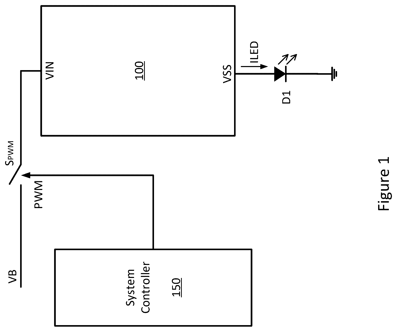
illustrates a block diagram of a light emitting diode system in accordance with various embodiments of the present disclosure;
illustrates a schematic diagram of a first implementation of the LED driver shown in in accordance with various embodiments of the present disclosure;
illustrates a schematic diagram of the PWM deglitch circuit shown in in accordance with various embodiments of the present disclosure;
illustrates various signals associated with the PWM deglitch circuit shown in in accordance with various embodiments of the present disclosure;
illustrates a schematic diagram of a second implementation of the LED driver shown in in accordance with various embodiments of the present disclosure;
illustrates a schematic diagram of a third implementation of the LED driver shown in in accordance with various embodiments of the present disclosure;
illustrates various signals associated with the LED driver shown in in accordance with various embodiments of the present disclosure;
illustrates a schematic diagram of a fourth implementation of the LED driver shown in in accordance with various embodiments of the present disclosure; and
illustrates a flow chart of a method for controlling the LED driver shown in in accordance with various embodiments of the present disclosure.
Corresponding numerals and symbols in the different figures generally refer to corresponding parts unless otherwise indicated. The figures are drawn to clearly illustrate the relevant aspects of the embodiments and are not necessarily drawn to scale.
DETAILED DESCRIPTION OF ILLUSTRATIVE EMBODIMENTS
The making and using of embodiments of this disclosure are discussed in detail below. It should be appreciated, however, that the concepts disclosed herein can be embodied in a wide variety of specific contexts, and that the specific embodiments discussed herein are merely illustrative and do not serve to limit the scope of the claims. Further, it should be understood that various changes, substitutions and alterations can be made herein without departing from the spirit and scope of this disclosure as defined by the appended claims.
Further, one or more features from one or more of the following described embodiments may be combined to create alternative embodiments not explicitly described, and features suitable for such combinations are understood to be within the scope of this disclosure. It is therefore intended that the appended claims encompass any such modifications or embodiments.
The present disclosure will be described with respect to embodiments in a specific context, namely an LED current overshoot reduction apparatus. The disclosure may also be applied, however, to a variety of LED systems. Hereinafter, various embodiments will be explained in detail with reference to the accompanying drawings.
illustrates a block diagram of a light emitting diode system in accordance with various embodiments of the present disclosure. As shown in , a PWM switch S PWM , an integrated circuit 100 and a light emitting diode D 1 are connected in series between a power source VB and ground. A system controller 150 is configured to generate a PWM signal (PWM) for controlling the PWM switch S PWM .
It should be noted that the block diagram shown in is merely an example. Depending on different applications and design needs, the system configuration may vary accordingly. For example, the light emitting diode D 1 may be placed between the PWM switch S PWM and the integrated circuit 100 . Furthermore, the PWM switch S PWM may be connected to ground directly. Under this system configuration, the PWM switch S PWM can be implemented as an n-type switch. The n-type switch typically has a lower on-resistance compared to a p-type switch for the same size, leading to lower voltage drops and higher efficiency in the light emitting diode system.
As shown in , a common node of the PWM switch S PWM and the integrated circuit 100 is labeled as VIN. A common node of the integrated circuit 100 and the light-emitting diode D 1 is labeled as VSS. The current flowing through the light-emitting diode D 1 is labeled as ILED. Throughout the description, ILED may be alternatively referred to as the LED current.
In some embodiments, the system controller 150 controls the PWM switch S PWM according to the power PWM dimming technique. In operation, the brightness of the light emitting diode D 1 can be controlled by varying the amount of time the light emitting diode D 1 is powered on and off. The brightness of the light emitting diode D 1 is determined by the ratio of the on-time to the off-time within each cycle. When the light emitting diode D 1 is powered on, the power source VB supplies power to the integrated circuit 100 through the turned-on PWM switch S PWM . When the light emitting diode D 1 is powered off, no power is supplied to the integrated circuit 100 . Under power PWM dimming, the light emitting diode D 1 , along with the integrated circuit 100 , is rapidly switched on and off at a high frequency. To ensure accurate and linear dimming, the delay time (e.g., soft start) from the PWM signal to the LED current response must be minimized. In a high frequency power PWM dimming process, soft start cannot be employed to lessen the fast PWM transition. The high frequency power PWM dimming process often leads to LED current overshoot. The present disclosure introduces four different implementations to reduce the LED current overshoot. These four different implementations to mitigate this LED current overshoot, which will be described in detail with respect to , 5 , 6 and 8 .
In some embodiments, the system controller 150 is implemented as a microcontroller. In alternative embodiments, the system controller 150 may be implemented as any suitable processors such as digital signal processing (DSP) controllers, field-programmable gate array (FPGA) processors and the like.
The PWM switch S PWM shown in may be implemented as n-type metal oxide semiconductor (NMOS) transistors. Alternatively, the switches may be implemented as other suitable controllable devices such as metal oxide semiconductor field effect transistor (MOSFET) devices, bipolar junction transistor (BJT) devices, super junction transistor (SJT) devices, insulated gate bipolar transistor (IGBT) devices, gallium nitride (GaN) based power devices, any combinations thereof and the like.
The integrated circuit 100 functions as an LED driver. Throughout the description, the integrated circuit 100 may be alternatively referred to as an LED driver 100 . In some embodiments, the LED driver 100 comprises a bias power supply, an undervoltage protection circuit, a reference circuit, a reference current generation circuit, a PWM deglitch circuit, a plurality of reference current paths, a precisely controlled current mirror, a power switch, a gate protection circuit and a startup circuit.
In some embodiments, the bias power supply is implemented as a low-dropout regulator. An input of the low-dropout regulator is configured to receive the voltage on VIN, and generate a bias voltage. The undervoltage protection circuit is implemented as an undervoltage lockout circuit. The undervoltage lockout circuit is configured to receive the bias voltage. Once the bias voltage is greater than a predetermined threshold, the undervoltage lockout circuit is configured to generate a control signal applied to the gate of the power switch in the LED driver 100 . A current flowing through the power switch is approximately equal to a current flowing through the light emitting diode D 1 . The reference circuit is implemented as a bandgap reference circuit. The bandgap reference circuit is configured to receive the bias voltage and generate a bandgap reference.
The reference current generation circuit is coupled between the bias voltage and VSS. The reference current generation circuit is configured to generate a predetermined reference current.
In a first implementation of the LED driver 100 , the LED driver 100 comprises a first reference current path. The first reference current path comprises a first switch. The predetermined reference current is mirrored to generate a first reference current in the first reference current path. Furthermore, the first reference current is mirrored to generate a load current flowing through the power switch in the LED driver 100 . The PWM deglitch circuit is configured to control the first switch so as to reduce an overshoot occurring at a leading-edge of the load current flowing through the power switch. The detailed structure and operating principle of the first implementation of the LED driver 100 will be described below with respect to .
In a second implementation of the LED driver 100 , the LED driver 100 comprises a first reference current path and a second reference current path. The second reference current path is connected in parallel with the first reference current path. The first reference current path comprises a first switch. The predetermined reference current is mirrored to generate a first reference current in the first reference current path and a second reference current in the second reference current path. Furthermore, a sum of the first reference current and the second reference current is mirrored to generate a load current flowing through the power switch in the LED driver 100 . The PWM deglitch circuit is configured to control the first switch so as to reduce an overshoot occurring at a leading-edge of a load current flowing through the power switch. The detailed structure and operating principle of the second implementation of the LED driver 100 will be described below with respect to .
In a third implementation of the LED driver 100 , the LED driver 100 comprises a first reference current path, a second reference current path, a third reference current path and a fourth reference current path. The second reference current path is connected in parallel with the first reference current path. The first reference current path comprises a first switch. The third reference current path comprises a second switch. The third reference current path is connected in parallel with the first reference current path. The fourth reference current path comprises a third switch. The fourth reference current path is connected in parallel with the first reference current path. The predetermined reference current is mirrored to generate a first reference current in the first reference current path, a second reference current in the second reference current path, a third reference current in the third reference current path and a fourth reference current in the fourth reference current path. Furthermore, a sum of the first reference current, the second reference current, the third reference current and the fourth reference current is mirrored to generate a load current flowing through the power switch. The PWM deglitch circuit is configured to control the first switch, the second switch and the third switch so as to reduce an overshoot occurring at a leading-edge of the load current flowing through the power switch. The detailed structure and operating principle of the third implementation of the LED driver 100 will be described below with respect to .
In a fourth implementation of the LED driver 100 , the LED driver 100 comprises a first reference current path, a second reference current path, a third reference current path, a fourth reference current path and a reference current subtraction circuit. The second reference current path is connected in parallel with the first reference current path. The first reference current path comprises a first switch. The third reference current path comprises a second switch. The third reference current path is connected in parallel with the first reference current path. The fourth reference current path comprises a third switch. The fourth reference current path is connected in parallel with the first reference current path. The predetermined reference current is mirrored to generate a first reference current in the first reference current path, a second reference current in the second reference current path, a third reference current in the third reference current path and a fourth reference current in the fourth reference current path. Furthermore, a sum of the first reference current, the second reference current, the third reference current and the fourth reference current is mirrored to generate a load current flowing through the power switch. The PWM deglitch circuit is configured to control the first switch, the second switch and the third switch so as to reduce an overshoot occurring at a leading-edge of the load current flowing through the power switch. Moreover, the reference current subtraction circuit is configured to subtract a current component from the sum of the reference currents. The reduced sum of the reference currents can further reduce the overshoot. The detailed structure and operating principle of the fourth implementation of the LED driver 100 will be described below with respect to .
It should be noted that the light emitting diode system shown in is merely an example. Depending on different applications and design needs, the system configuration may vary accordingly. For example, a current sense resistor may be placed between the light emitting diode and ground. Furthermore, while illustrates one light emitting diode, the light emitting diode system could accommodate any number of light emitting diodes connected in series and/or parallel.
illustrates a schematic diagram of a first implementation of the LED driver shown in in accordance with various embodiments of the present disclosure. The LED driver comprises a low-dropout regulator 202 , an undervoltage lockout circuit 204 , a bandgap reference circuit 206 , a PWM deglitch circuit 208 , a reference current generation circuit 222 , a first reference current path 231 , a power switch Q 1 , a precisely controlled current mirror 228 , a gate protection circuit 224 and a startup circuit 226 .
As shown in , an input of the low-dropout regulator 202 is configured to receive an input voltage VIN. The low-dropout regulator 202 is configured to generate a bias voltage VDD. Throughout the description, the voltage bus on which the bias voltage VDD is generated may be alternatively referred to as a first voltage bus. The voltage bus labeled as VSS may be alternatively referred to as a second voltage bus.
The undervoltage lockout circuit 204 is configured to receive the bias voltage VDD. Once the bias voltage VDD is greater than a predetermined threshold, the undervoltage lockout circuit 204 is configured to generate a control signal applied to a gate of the power switch Q 1 . This control signal keeps the power switch Q 1 on. In other words, the control signal functions as a power good (PG) signal.
The bandgap reference circuit 206 is configured to receive the bias voltage VDD and generate a bandgap reference VBG. The bandgap reference VBG is used to set up a reference current IREF as shown in .
The reference current generation circuit 222 comprises a first p-type transistor MP 1 , a resistor R SET and a first amplifier 212 . The first p-type transistor MP 1 and the resistor R SET are connected in series between the first voltage bus VDD and the second voltage bus VSS. An inverting input of the first amplifier 212 is configured to receive the bandgap reference VBG. A non-inverting input of the first amplifier 212 is connected to a common node of the first p-type transistor MP 1 and the resistor R SET . The voltage on the common node of the first p-type transistor MP 1 and the resistor R SET is labeled as VREF as shown in . An output of the first amplifier 212 is connected to a gate of the first p-type transistor MP 1 .
In operation, the first amplifier 212 forces the voltage on the node VREF to be equal to the bandgap reference VBG. The current flowing through the resistor R SET is equal to the bandgap reference VBG divided by the resistance value of R SET . This current is the reference current IREF of the LED driver. Throughout the description, the voltage on the node VREF may be alternatively referred to as a reference voltage signal.
The first reference current path 231 comprises a second p-type transistor MP 2 and a first switch S 1 connected in series between the first voltage bus VDD and a voltage node VDA. The gate of the first switch S 1 is controlled by the PWM deglitch circuit 208 .
In operation, the first p-type transistor MP 1 and the second p-type transistor MP 2 form a first current mirror. Through the first current mirror, the reference current IREF generated by the reference current generation circuit 222 is mirrored to generate a first reference current IREF 1 in the first reference current path 231 .
The precisely controlled current mirror 228 comprises a first n-type transistor MN 1 , a second n-type transistor MN 2 and a second amplifier 214 . As shown in , the first n-type transistor MN 1 and the first reference current path 231 are connected in series between the second voltage bus VSS and the first voltage bus VIN. The second n-type transistor MN 2 is connected in series with the power switch Q 1 . An inverting input of the second amplifier 214 is connected to a drain of the first n-type transistor MN 1 . The drain of the first n-type transistor MN 1 is labeled as VDA as shown in . A non-inverting input of the second amplifier 214 is connected to a drain of the second n-type transistor MN 2 . The drain of the second n-type transistor MN 2 is labeled as VDB as shown in . An output of the second amplifier 214 is connected to the gate of the first n-type transistor MN 1 and the gate of the second n-type transistor MN 2 .
In operation, the second amplifier 214 forces the voltage on the drain of the first n-type transistor MN 1 to be equal to the voltage on the drain of the second n-type transistor MN 2 . Such a voltage relationship helps to achieve a precisely controlled current mirror. Through the precisely controlled current mirror 228 , the first reference current IREF 1 in the first reference current path 231 is mirrored to generate the load current IL flowing through the power switch Q 1 . In some embodiments, the ratio of the current flowing through the second n-type transistor MN 2 to the current flowing through the first n-type transistor MN 1 is in a range from about 1000 to about 10,000. Throughout the description, the precisely controlled current mirror 228 may be alternatively referred to as a second current mirror.
The PWM deglitch circuit 208 is configured to receive the voltage on the voltage node VREF. This voltage is proportional to the reference current IREF. Based on the received voltage on VREF, the PWM deglitch circuit 208 is configured to generate a plurality of control signals for controlling switches in different reference current paths so as to reduce an overshoot occurring at a leading-edge of a load current flowing through the power switch Q 1 . In the first implementation of the LED driver shown in , the PWM deglitch circuit 208 generates a control signal at a first terminal T 1 . This control signal is applied to the gate of the first switch S 1 to reduce the overshoot of the load current IL.
In operation, PWM switching often introduces transient noise to the functional blocks of the LED driver (e.g., low-dropout regulator 202 and/or and bandgap reference circuit 206 ). During switching or power-up, the transient noise can lead to the overshoot of the load current flowing through the power switch Q 1 . The PWM deglitch circuit 208 is able to detect the transient noise on the node VREF, and convert the transient noise into a digital signal to control the on and off of the first switch S 1 . More particularly, when the transient noise occurs at the node VREF, the PWM deglitch circuit 208 converts the transient noise into a logic high signal to turn off the first switch S 1 . Once the first switch S 1 is temporarily turned off, the first reference current IREF 1 is reduced, thereby reducing the overshoot of the load current IL flowing through the power switch Q 1 .
The load current path of the LED driver comprises the power switch Q 1 . The load current IL flows through the power switch Q 1 . The LED current ILED includes some bias currents (e.g., IREF). Since the bias currents of the LED driver are quite small, the load current IL is approximately equal to the LED current ILED.
The gate protection circuit 224 is connected between the gate of the power switch Q 1 and the second voltage bus VSS. The gate protection circuit 224 comprises a first resistor R 1 , a second resistor R 2 , a capacitor C 1 and a third n-type transistor MN 3 . The third n-type transistor MN 3 is connected between the gate of the power switch Q 1 and the second voltage bus VSS. The first resistor R 1 and the capacitor C 1 are connected in series between the gate of the power switch Q 1 and the second voltage bus VSS. The second resistor R 2 is connected between the gate of the power switch Q 1 and the second voltage bus VSS.
In operation, the gate protection circuit 224 serves two functions. First, the capacitor C 1 , the first resistor R 1 and the third n-type transistor MN 3 form a voltage clamping circuit configured to provide various protections such as electrostatic discharge (ESD) and electrical overstress (EOS) protection. When there is a fast voltage event from the input voltage bus VIN, such as ESD or power switching, a high-voltage transient can travel from the drain terminal of the power switch Q 1 to its gate through the parasitic Miller capacitance of the power switch Q 1 . This fast transient can turn on the third n-type transistor MN 3 , thereby keeping the gate voltage of Q 1 at a safe level. Second, the second resistor R 2 provides a passive pulldown for the power switch Q 1 , helping the undervoltage lockout circuit 204 keep the power switch Q 1 off when the LED drive operates in an undervoltage condition.
The startup circuit 226 comprises a third current mirror comprising a fourth n-type transistor MN 4 and a fifth n-type transistor MN 5 . The startup circuit 226 further comprises a sixth p-type transistor MP 6 . As shown in , the sixth p-type transistor MP 6 and the fifth n-type transistor MN 5 are connected in series between the first voltage bus VDD and the second voltage bus VSS. The power switch Q 1 and the fourth n-type transistor MN 4 are connected in series between the input voltage bus VIN and the second voltage bus VSS. The gate of the sixth p-type transistor MP 6 is connected to the gate of the first p-type transistor MP 1 . The reference current IREF is mirrored to generate a current flowing through the sixth p-type transistor MP 6 .
In operation, the precisely controlled current mirror 228 has multiple stable states. The startup circuit 226 ensures that an initial current flows, prompting the precisely controlled current mirror 228 to enter its correct operating state.
illustrates a schematic diagram of the PWM deglitch circuit shown in in accordance with various embodiments of the present disclosure. The PWM deglitch circuit 208 comprises a first inverter 311 , a second inverter 312 , a current source IB, a leading-edge blanking circuit 302 , an XOR gate 304 , an inverter 306 and an NOR gate 308 . The first inverter 311 is formed by a p-type transistor M 1 and an n-type transistor M 2 connected in series between VDD and VSS. The second inverter 312 is formed by a p-type transistor M 3 and an n-type transistor M 4 connected in series between VDD and VSS.
As shown in , the first inverter 311 is configured to receive the reference voltage signal VREF. The reference voltage signal VREF is proportional to the reference current IREF. In some embodiments, the threshold voltage of the first inverter 311 is selected such that the first inverter 311 switches its output from a logic high state to a logic low state when VREF exceeds its target or steady state value. In other words, the steady state value of VREF may be selected as the threshold voltage of the first inverter 311 . Once VREF is greater than this threshold voltage, the first inverter generates a logic low signal fed into the second inverter 312 .
As shown in , the second inverter 312 has an input connected to the output of the first inverter 311 . The output of the second inverter 312 is configured to generate a first control signal applied to a first terminal T 1 . Referring back to , T 1 is connected to the gate of the first switch S 1 . When an overshoot occurs, the leading-edge portion of VREF exceeds the steady state value of VREF. In response to this, the first inverter 311 generates a logic low signal. The second inverter 312 converts this logic low signal into a logic high signal applied to the gate of the first switch S 1 . Since the first switch S 1 is a p-type transistor, the logic high signal turns off the first switch S 1 . Referring back to , once the first switch S 1 is turned off, the current flowing through the power switch Q 1 is reduced. The reduced load current helps reduce the overshoot of the LED current ILED.
The leading-edge blanking circuit 302 may comprise a timer, an inverter and an AND gate. The current source IB provides a bias current for the timer. The timer is configured to generate a blanking pulse in response to the leading-edge of VREF. The blanking pulse is fed into the inverter. A first input of the AND gate is configured to receive the first control signal (T 1 ). A second input of the AND gate is configured to receive the output signal of the inverter. In this way, the AND gate only allows the first control signal to pass through and reach the third terminal T 3 after the blanking period is over. The signal generated at the third terminal T 3 is a third control signal. The third control signal will be described in detail below with respect to .
The XOR gate 304 , the inverter 306 and the NOR gate 308 are connected in cascade as shown in . A first input of the XOR gate 304 is configured to receive the first control signal (T 1 ). A second input of the XOR gate 304 is configured to receive the third control signal (T 3 ). An input of the inverter 306 is connected to an output of the XOR gate 304 . A first input of the NOR gate 308 is configured to receive the third control signal (T 3 ). A second input of the NOR gate 308 is connected to an output of the inverter 306 . An output of the NOR gate 308 is configured to generate a control signal at the second terminal T 2 . The signal generated at the second terminal T 2 is a second control signal. The second control signal will be described in detail below with respect to .
In response to an overshoot of VREF, the PWM deglitch circuit 208 is able to generate three control signals. The duration of the logic high state of the first control signal (T 1 ) is approximately equal to the duration of the overshoot of VREF. The first control signal is simultaneously divided into two portions. The leading portion is the second control signal (T 2 ). The trailing portion is the third control signal (T 3 ). These three control signals function as three control variables to turn off corresponding reference current paths, thereby reducing the overshoot of the load current IL flowing through the power switch Q 1 .
illustrates various signals associated with the PWM deglitch circuit shown in in accordance with various embodiments of the present disclosure. The horizontal axis represents intervals of time. There are five rows. The first row represents the PWM signal shown in . The second row represents the reference voltage signal VREF. The third row represents the first control signal T 1 . The fourth row represents the second control signal T 2 . The fifth row represents the third control signal T 3 .
At t1, the PWM signal changes from a logic low state to a logic high state. In response to this change, the PWM switch is turned on and power is supplied to the LED driver. After a suitable circuit delay, the reference voltage signal VREF starts to establish from t2. As shown in , an overshoot of VREF occurs. At t3, the overshoot exceeds the threshold voltage VTH of the first inverter 311 . The first inverter 311 and the second inverter 312 collectively function as a buffer. From t3 to t5, the overshoot is greater than threshold voltage VTH. As a result, the first control signal (T 1 ) is of a logic high state from t3 to t5. Referring back to , through the XOR gate 304 , the inverter 306 and the NOR gate 308 , the leading portion (from t3 to t4) of the first control signal (T 1 ) is generated as the second control signal (T 2 ). Through the leading-edge blanking circuit 302 , the trailing portion (from t4 to t5) of the first control signal (T 1 ) is generated as the third control signal (T 3 ).
illustrates a schematic diagram of a second implementation of the LED driver shown in in accordance with various embodiments of the present disclosure. The second implementation of the LED driver is similar to the first implementation of the LED driver shown in except that a second reference current path 232 is added. As shown in , the second reference current path 232 is connected in parallel with the first reference current path 231 . The second reference current path 232 comprises a third p-type transistor MP 3 . The reference current IREF is mirrored to generate a second reference current IREF 2 in the second reference current path 232 . A sum of the first reference current IREF 1 and the second reference current IREF 2 is mirrored to generate the load current IL flowing through the power switch Q 1 .
The second reference current path 232 does not comprise a switch controlled by the PWM deglitch circuit 208 . In operation, the second reference current IREF 2 in the second reference current path 232 is unchanged. The PWM deglitch circuit 208 can only partially cancel the overshoot through turning off the first switch S 1 in the first reference current path 231 .
illustrates a schematic diagram of a third implementation of the LED driver shown in in accordance with various embodiments of the present disclosure. The third implementation of the LED driver is similar to the second implementation of the LED driver shown in except that a third reference current path 233 and a fourth reference current path 234 are added to further improve the performance of the LED driver.
As shown in , the third reference current path 233 is connected in parallel with the first reference current path 231 . The third reference current path 233 comprises a fourth p-type transistor MP 4 and a second switch S 2 connected in series. The second switch S 2 is implemented as a p-type transistor. The second switch S 2 is controlled by the PWM deglitch circuit 208 .
The fourth reference current path 234 is connected in parallel with the first reference current path 231 . The fourth reference current path 234 comprises a fifth p-type transistor MP 5 and a third switch S 3 connected in series. The third switch S 3 is implemented as a p-type transistor. The third switch S 3 is controlled by the PWM deglitch circuit 208 .
In operation, the reference current IREF is mirrored to generate a first reference current IREF 1 in the first reference current path 231 . The reference current IREF is mirrored to generate a second reference current IREF 2 in the second reference current path 232 . The reference current IREF is mirrored to generate a third reference current IREF 3 in the third reference current path 233 . The reference current IREF is mirrored to generate a fourth reference current IREF 4 in the fourth reference current path 234 . A sum of the first reference current IREF 1 , the second reference current IREF 2 , the third reference current IREF 3 and the fourth reference current IREF 4 is mirrored to generate the load current IL flowing through the power switch Q 1 . In response to the overshoot of the reference voltage signal VREF, the PWM deglitch circuit 208 is configured to turn off the control switches S 1 , S 2 and S 3 so as to reduce the sum of the reference currents, thereby reducing the overshoot of the load current IL flowing through the power switch Q 1 .
illustrates various signals associated with the LED driver shown in in accordance with various embodiments of the present disclosure. The horizontal axis represents intervals of time. There are three rows. The first row represents the PWM signal. The second row represents the LED current (LED_P) when a conventional LED driver is employed to drive a light emitting diode. The third row represents the LED current (LED_N) when the LED driver shown in is employed to drive the light emitting diode.
At t1, the PWM signal changes from a logic low state to a logic high state. In response to this change, the PWM switch is turned on and power is supplied to the LED driver. After a suitable circuit delay, the LED current starts to establish at t2. When a conventional LED driver is employed to drive a light emitting diode, there is an overshoot from t2 to t3. As shown in , the LED current rapidly increases to a peak, remains constant for a period, and then begins to linearly decrease to its steady-state value. In contrast, when the LED driver shown in is employed to drive the light emitting diode, the LED current increases in a linear manner to an intermediate value, and then curves downward to a first valley. From the first valley, the LED current increases to a first peak, and then linearly decreases to a second valley. From the second valley, the LED current increases to a second peak, and then begins to linearly decrease to its steady-state value. The peak (e.g., the second peak) in the third row is much lower than the peak in the second row.
illustrates a schematic diagram of a fourth implementation of the LED driver shown in in accordance with various embodiments of the present disclosure. The fourth implementation of the LED driver is similar to the third implementation of the LED driver shown in except that a reference current subtraction circuit 802 is added to further improve the performance of the LED driver.
The reference current subtraction circuit 802 comprises a first current subtraction transistor M 11 , a rise detection capacitor C 11 , a rise detection resistor R 11 , a second current subtraction transistor M 12 , a fall detection resistor R 12 and a fall detection capacitor C 12 .
As shown in , the first current subtraction transistor M 11 is connected between the drain of the first n-type transistor MN 1 and the second voltage bus VSS. The rise detection capacitor C 11 and the rise detection resistor R 11 are connected in series between the common node of the first p-type transistor MP 1 and the resistor R SET , and the second voltage bus VSS. A common node of the rise detection capacitor C 11 and the rise detection resistor R 11 is connected to the gate of the first current subtraction transistor M 11 .
The second current subtraction transistor M 12 is connected between the drain of the first n-type transistor MN 1 and the second voltage bus VSS. The fall detection resistor R 12 and the fall detection capacitor C 12 are connected in series between the common node of the first p-type transistor MP 1 and the resistor R SET , and the second voltage bus VSS. The common node of the fall detection resistor R 12 and the fall detection capacitor C 12 is connected to the gate of the second current subtraction transistor M 12 .
In operation, the reference current subtraction circuit 802 is configured to subtract a current component from the sum of the reference currents, thereby reducing the overshoot occurring at the leading-edge of the load current IL. The rise detection capacitor C 11 and the rise detection resistor R 11 set the delay timing for the rising section of the overshoot signal, while the fall detection resistor R 12 and the fall detection capacitor C 12 set the delay timing for the falling section of the overshoot signal. To further improve the subtraction amplitude, simply adjust the channel widths of the first current subtraction transistor M 11 and the second current subtraction transistor M 12 .
illustrates a flow chart of a method for controlling the LED driver shown in in accordance with various embodiments of the present disclosure. This flowchart shown in is merely an example, which should not unduly limit the scope of the claims. One of ordinary skill in the art would recognize many variations, alternatives, and modifications. For example, various steps illustrated in may be added, removed, replaced, rearranged and repeated.
At step 902 , a predetermined reference current is generated using a reference current generation circuit coupled between a first voltage bus and a second voltage bus.
At step 904 , the predetermined reference current is mirrored to generate a first reference current in a first reference current path comprising a first switch.
At step 906 , the first switch is controlled by a PWM deglitch circuit to reduce an overshoot occurring at a leading-edge of a load current flowing through a power switch.
The method further comprises mirroring the predetermined reference current to generate a second reference current in a second reference current path, and mirroring a sum of the first reference current and the second reference current to generate the load current flowing through the power switch, wherein the second reference current path is connected in parallel with the first reference current path.
The method further comprises mirroring the predetermined reference current to generate a second reference current in a second reference current path, mirroring the predetermined reference current to generate a third reference current in a third reference current path, mirroring the predetermined reference current to generate a fourth reference current in a fourth reference current path, and mirroring a sum of the first reference current, the second reference current, the third reference current and the fourth reference current to generate the load current flowing through the power switch, and wherein the second reference current path is connected in parallel with the first reference current path, the third reference current path is connected in parallel with the first reference current path, and wherein the third reference current path comprises a second switch controlled by the PWM deglitch circuit, and the fourth reference current path is connected in parallel with the first reference current path, wherein the fourth reference current path comprises a third switch controlled by the PWM deglitch circuit.
The reference current generation circuit comprises a first p-type transistor and a resistor connected in series between the first voltage bus and the second voltage bus, and a first amplifier having an inverting input configured to receive a bandgap reference, a non-inverting input connected to a common node of the first p-type transistor and the resistor and an output connected to a gate of the first p-type transistor and a gate of a second p-type transistor, the first reference current path comprises the second p-type transistor and the first switch connected in series, and wherein the first p-type transistor and the second p-type transistor form a first current mirror through which the predetermined reference current is mirrored to generate the first reference current in the first reference current path, and a second current mirror comprises a first n-type transistor connected in series with the first reference current path, a second n-type transistor connected in series with the power switch, wherein the first n-type transistor and the second n-type transistor form a second current mirror through which the sum of the first reference current, the second reference current, the third reference current and the fourth reference current is mirrored to generate the load current flowing through the power switch, and a second amplifier having an inverting input connected to a drain of the first n-type transistor, a non-inverting input connected to a drain of the second n-type transistor and an output connected to a gate of the first n-type transistor and a gate of the second n-type transistor.
The PWM deglitch circuit comprises a first inverter configured to receive a reference voltage signal proportional to the predetermined reference current, a second inverter having an input connected to an output of the first inverter and an output configured to generate a first control signal applied to a gate of the first switch, a leading-edge blanking circuit having an input configured to receive the first control signal and an output configured to generate a third control signal applied to a gate of the third switch, and an XOR gate, an inverter and an NOR gate connected in cascade, wherein a first input of the XOR gate is configured to receive the first control signal, a second input of the XOR gate is configured to receive the third control signal, an input of the inverter is connected to an output of the XOR gate, a first input of the NOR gate is configured to receive the third control signal, a second input of the NOR gate is connected to an output of the inverter, and an output of the NOR gate is configured to generate a second control signal applied to a gate of the second switch.
Although the description has been described in detail, it should be understood that various changes, substitutions and alterations can be made without departing from the spirit and scope of this disclosure as defined by the appended claims. Moreover, the scope of the disclosure is not intended to be limited to the particular embodiments described herein, as one of ordinary skill in the art will readily appreciate from this disclosure that processes, machines, manufacture, compositions of matter, means, methods, or steps, presently existing or later to be developed, which may perform substantially the same function or achieve substantially the same result as the corresponding embodiments described herein, may be utilized according to the present disclosure. Accordingly, the appended claims are intended to include within their scope such processes, machines, manufacture, compositions of matter, means, methods, or steps.
Figures (9)
Citations
This patent cites (10)
- US10542593
- US11849514
- US12477631
- US2009/0189539
- US2009/0195191
- US2010/0090755
- US2013/0015780
- US2019/0380180
- US102740564
- US106304460