Semiconductor Integrated Circuit and Receiver Device
Abstract
A semiconductor integrated circuit includes a first input terminal inputting a first signal, a second input terminal supplied to a first voltage, an output terminal outputting a second signal. The circuit includes: a first transistor having first, second, control terminals respectively connected to a first node, the output terminal and first input terminals; a second transistor having first, second, control terminals respectively connected to the first and second nodes, the output terminal; a third transistor having a first terminal supplied to a second voltage, second and control terminals respectively connected to the first node and the second input terminal; a fourth transistor having first and control terminals respectively connected to the output terminal and the second node, a second terminal supplied to a third voltage; and a fifth transistor having first and control terminals connected to the second node, and a second terminal supplied to the third voltage.
Claims (20)
1 . A semiconductor integrated circuit comprising a first buffer having a first input terminal to which a first signal is input, a second input terminal to which a first voltage is supplied, and a first output terminal from which a second signal is output, wherein the first buffer includes: a first transistor having a first terminal connected to a first node, a second terminal connected to the first output terminal, and a control terminal connected to the first input terminal; a second transistor having a first terminal connected to the first node, a second terminal connected to a second node, and a control terminal connected to the first output terminal; a third transistor having a first terminal to which a second voltage is supplied, a second terminal connected to the first node, and a control terminal connected to the second input terminal; a fourth transistor having a first terminal connected to the first output terminal, a second terminal to which a third voltage is supplied, and a control terminal connected to the second node; a fifth transistor having a first terminal and a control terminal each connected to the second node, and a second terminal to which the third voltage is supplied; and a sixth transistor or a third capacitor, the sixth transistor having a first terminal to which the second voltage is supplied, a second terminal connected to the first output terminal, and a control terminal connected to the first node, the third capacitor having a first terminal connected to the first node and a second terminal connected to the first output terminal.
Show 19 dependent claims
2 . The semiconductor integrated circuit according to claim 1 , wherein the first buffer further has a third input terminal to which a third signal constituting differential signals with the first signal is input, and the first buffer further includes: a seventh transistor having a first terminal to which the second voltage is supplied, a second terminal connected to the first output terminal, and a control terminal connected to the third input terminal; and a first current source having an input terminal connected to the first output terminal and an output terminal to which the third voltage is supplied.
3 . The semiconductor integrated circuit according to claim 1 , further comprising a second buffer having a third input terminal to which a third signal constituting differential signals with the first signal is input, a fourth input terminal to which the first voltage is supplied, and a second output terminal from which a fourth signal constituting differential signals with the second signal is output, wherein the second buffer includes: an eighth transistor having a first terminal connected to a third node, a second terminal connected to the second output terminal, and a control terminal connected to the third input terminal; a ninth transistor having a first terminal connected to the third node, a second terminal connected to a fourth node, and a control terminal connected to the second output terminal; a tenth transistor having a first terminal to which the second voltage is supplied, a second terminal connected to the third node, and a control terminal connected to the fourth input terminal; an eleventh transistor having a first terminal connected to the second output terminal, a second terminal to which the third voltage is supplied, and a control terminal connected to the fourth node; and a twelfth transistor having a first terminal and a control terminal each connected to the fourth node, and a second terminal to which the third voltage is supplied.
4 . The semiconductor integrated circuit according to claim 3 , wherein the first buffer further includes a first capacitor having a first terminal connected to the second input terminal and a second terminal connected to the third node, and the second buffer further includes a second capacitor having a first terminal connected to the fourth input terminal and a second terminal connected to the first node.
5 . The semiconductor integrated circuit according to claim 3 , further comprising: a first converter configured to determine a first bit string from the second signal and the fourth signal based on a first clock signal; and a second converter configured to determine a second bit string from the second signal and the fourth signal based on a second clock signal shifted from the first clock signal by a first phase.
6 . The semiconductor integrated circuit according to claim 5 , wherein each of the first converter and the second converter is a successive approximation register AD converter.
7 . The semiconductor integrated circuit according to claim 1 , wherein the first transistor, the fourth transistor, and the fifth transistor have a first conductivity type, and the second transistor and the third transistor have a second conductivity type different from the first conductivity type.
8 . The semiconductor integrated circuit according to claim 7 , wherein the first conductivity type is an N-conductivity type, the second conductivity type is a P-conductivity type, and the second voltage is higher than the third voltage.
9 . The semiconductor integrated circuit according to claim 7 , wherein the first conductivity type is a P-conductivity type, the second conductivity type is an N-conductivity type, and the third voltage is higher than the second voltage.
10 . The semiconductor integrated circuit according to claim 1 , wherein the first buffer is a source follower.
11 . A receiver device comprising: the semiconductor integrated circuit according to claim 1 ; and a processing circuit configured to process a signal output from the semiconductor integrated circuit.
12 . The receiver device according to claim 11 , wherein the first buffer further has a third input terminal to which a third signal constituting differential signals with the first signal is input, and the first buffer further includes: a seventh transistor having a first terminal to which the second voltage is supplied, a second terminal connected to the first output terminal, and a control terminal connected to the third input terminal; and a first current source having an input terminal connected to the first output terminal and an output terminal to which the third voltage is supplied.
13 . The receiver device according to claim 11 , further comprising a second buffer having a third input terminal to which a third signal constituting differential signals with the first signal is input, a fourth input terminal to which the first voltage is supplied, and a second output terminal from which a fourth signal constituting differential signals with the second signal is output, wherein the second buffer includes: an eighth transistor having a first terminal connected to a third node, a second terminal connected to the second output terminal, and a control terminal connected to the third input terminal; a ninth transistor having a first terminal connected to the third node, a second terminal connected to a fourth node, and a control terminal connected to the second output terminal; a tenth transistor having a first terminal to which the second voltage is supplied, a second terminal connected to the third node, and a control terminal connected to the fourth input terminal; an eleventh transistor having a first terminal connected to the second output terminal, a second terminal to which the third voltage is supplied, and a control terminal connected to the fourth node; and a twelfth transistor having a first terminal and a control terminal each connected to the fourth node, and a second terminal to which the third voltage is supplied.
14 . The receiver device according to claim 13 , wherein the first buffer further includes a first capacitor having a first terminal connected to the second input terminal and a second terminal connected to the third node, and the second buffer further includes a second capacitor having a first terminal connected to the fourth input terminal and a second terminal connected to the first node.
15 . The receiver device according to claim 13 , further comprising: a first converter configured to determine a first bit string from the second signal and the fourth signal based on a first clock signal; and a second converter configured to determine a second bit string from the second signal and the fourth signal based on a second clock signal shifted from the first clock signal by a first phase.
16 . The receiver device according to claim 15 , wherein each of the first converter and the second converter is a successive approximation register AD converter.
17 . The receiver device according to claim 11 , wherein the first transistor, the fourth transistor, and the fifth transistor have a first conductivity type, and the second transistor and the third transistor have a second conductivity type different from the first conductivity type.
18 . The receiver device according to claim 17 , wherein the first conductivity type is an N-conductivity type, the second conductivity type is a P-conductivity type, and the second voltage is higher than the third voltage.
19 . The receiver device according to claim 17 , wherein the first conductivity type is a P-conductivity type, the second conductivity type is an N-conductivity type, and the third voltage is higher than the second voltage.
20 . The receiver device according to claim 11 , wherein the first buffer is a source follower.
Full Description
Show full text →
CROSS-REFERENCE TO RELATED APPLICATIONS
This application is based upon and claims the benefit of priority from Japanese Patent Application No. 2023-041277, filed Mar. 15, 2023, the entire contents of which are incorporated herein by reference.
FIELD
Embodiments described herein relate generally to a semiconductor integrated circuit and a receiver device.
BACKGROUND
A transmitter device and a receiver device are connected via a transmission path. The transmitter device superimposes data on an analog signal and outputs the analog signal. The receiver device receives the analog signal that has passed through the transmission path. The receiver device includes a semiconductor integrated circuit that processes the analog signal. The receiver device generates a digital signal based on the analog signal. The receiver device recovers the data based on the generated digital signal.
BRIEF DESCRIPTION OF DRAWINGS
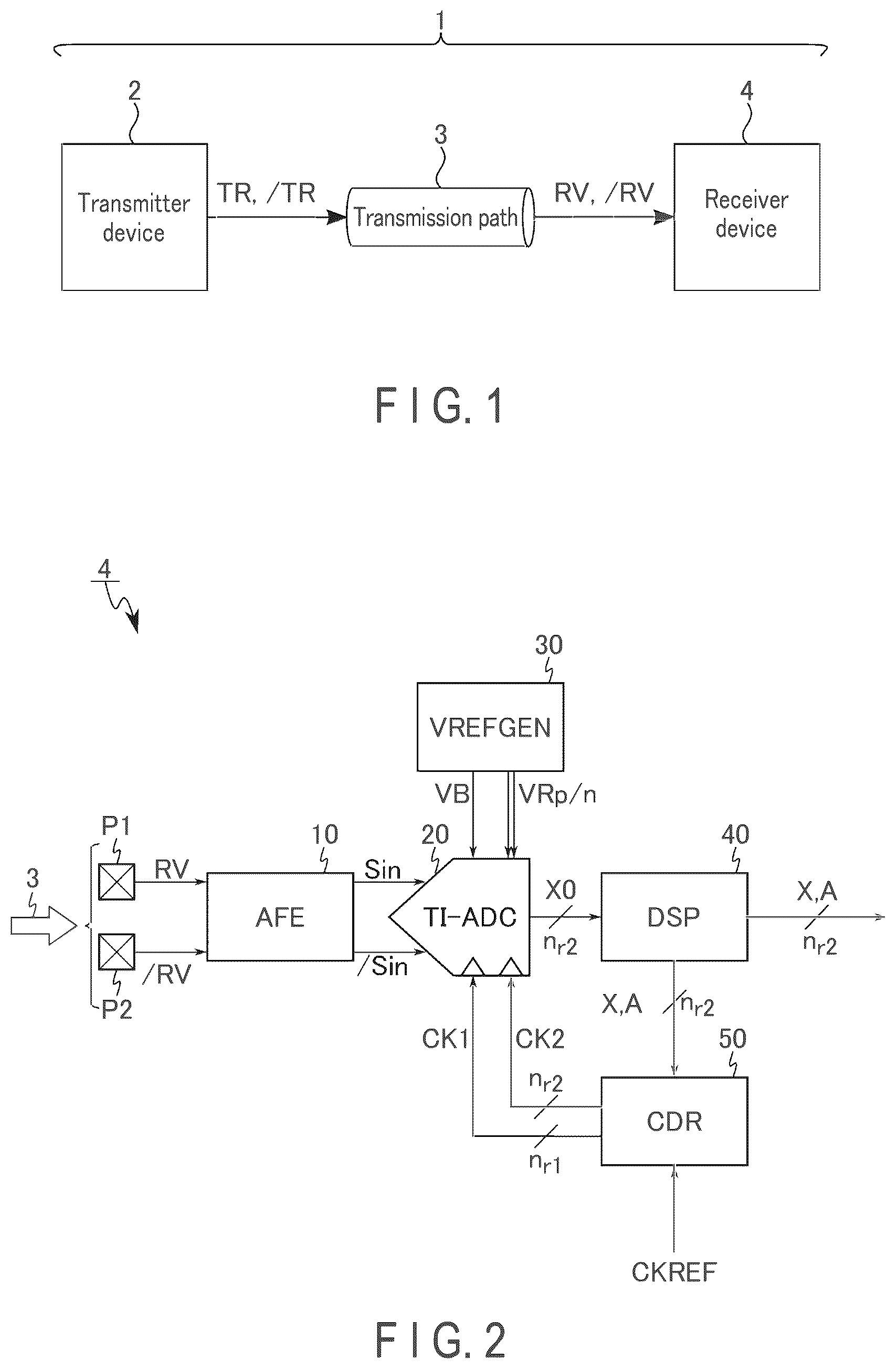
is a block diagram illustrating an example of a configuration of a communication system including a receiver device according to an embodiment.
is a block diagram illustrating an example of a configuration of a receiver circuit included in the receiver device according to the embodiment.
is a block diagram illustrating an example of a configuration of an AD converter included in the receiver circuit according to the embodiment.
is a block diagram illustrating an example of a configuration of a buffer included in the AD converter according to the embodiment.
is a circuit diagram illustrating an example of a configuration of the buffer included in the AD converter according to the embodiment.
is a circuit diagram illustrating an example of a configuration of a buffer included in an AD converter according to a modification.
DETAILED DESCRIPTION
In general, according to one embodiment, a semiconductor integrated circuit includes a first buffer having a first input terminal to which a first signal is input, a second input terminal to which a first voltage is supplied, and a first output terminal from which a second signal is output. The first buffer includes a first transistor, a second transistor, a third transistor, a fourth transistor, and a fifth transistor. The first transistor has a first terminal connected to a first node, a second terminal connected to the first output terminal, and a control terminal connected to the first input terminal. The second transistor has a first terminal connected to the first node, a second terminal connected to a second node, and a control terminal connected to the first output terminal. The third transistor has a first terminal to which a second voltage is supplied, a second terminal connected to the first node, and a control terminal connected to the second input terminal. The fourth transistor has a first terminal connected to the first output terminal, a second terminal to which a third voltage is supplied, and a control terminal connected to the second node. The fifth transistor has a first terminal and a control terminal each connected to the second node, and a second terminal to which the third voltage is supplied.
Embodiments will be described below with reference to the drawings.
Note that, in the following description, components having substantially the same functions and configurations are denoted by the same reference numerals. In a case where elements having similar configurations are particularly distinguished from each other, letters or numbers different from each other may be added to the ends of the same reference numerals.
1. Embodiment
An embodiment will be described.
1.1 Communication System
A configuration of a communication system including a receiver device according to the embodiment will first be described. is a block diagram illustrating an example of a configuration of the communication system including the receiver device according to the embodiment.
A communication system 1 is configured to transmit data from one device or circuit to another device or circuit by high-speed serial communication. Specifically, for example, the communication system 1 achieves a communication speed of 128 Gbps. The communication system 1 includes a transmitter device 2 , a transmission path 3 , and a receiver device 4 . The communication system 1 may be constituted by a plurality of devices or circuits provided on the same printed circuit board, or may be constituted by a plurality of devices or circuits provided on different printed circuit board.
The transmitter device 2 is configured to transmit signals TR and /TR to the receiver device 4 via the transmission path 3 . The signals TR and /TR are differential signals. The signals TR and /TR are, for example, signals including a plurality of pulse signals. Data is superimposed on each pulse signal of the signals TR and /TR. The voltage level of each pulse signal of the signals TR and /TR corresponds to data of one or more bits. The data superimposed on the pulse signal is transmitted from the transmitter device 2 to the receiver device 4 via the transmission path 3 .
The transmission path 3 is a physical or spatial transmission medium for transmitting the signals TR and /TR to the receiver device 4 . The transmission path 3 is, for example, wiring that connects the transmitter device 2 and the receiver device 4 . The transmission path 3 may have various transmission characteristics depending on the structure and material of the transmission medium. The transmission characteristics of the transmission path 3 have, for example, a frequency characteristic with a loss of gain in a specific frequency band.
The signals TR and /TR transmitted by the transmitter device 2 pass through the transmission path 3 , thereby suffering a loss corresponding to the transmission characteristics of the transmission path 3 . Thus, inter-symbol interference (ISI) occurs in the signals TR and /TR that have passed through the transmission path 3 . Therefore, the signals TR and /TR that have passed through the transmission path 3 are processed as analog signals in an initial stage circuit of the receiver device 4 . In the following, the signals TR and /TR that have passed through the transmission path 3 and have suffered loss are referred to as signals RV and /RV.
The receiver device 4 is configured to receive the signals RV and /RV from the transmitter device 2 via the transmission path 3 . The receiver device 4 decodes the data superimposed on the signals TR and /TR by the transmitter device 2 based on the signals RV and /RV. The receiver device 4 has a receiver circuit for correctly decoding data superimposed on the signals TR and /TR. The receiver circuit may be referred to as a semiconductor integrated circuit.
1.2 Receiver Circuit
is a block diagram illustrating an example of a configuration of a receiver circuit of the receiver device according to the embodiment.
The receiver device 4 includes, for example, pads P 1 and P 2 , a AFE 10 , a TI-ADC 20 , a VREFGEN 30 , a DSP 40 , and a CDR 50 as a receiver circuit.
Each of the pads P 1 and P 2 is a terminal connected to the transmission path 3 . The example of illustrates a case where the pads P 1 and P 2 receive the signals RV and /RV, respectively, from the transmitter device 2 via the transmission path 3 .
The AFE 10 is an analog front end. The AFE 10 includes, for example, a continuous time linear equalizer (CTLE) and a variable gain amplifier (VGA). The CTLE is an amplifier circuit having a frequency characteristic that compensates for the frequency characteristic of the transmission path 3 . The VGA is an amplifier circuit capable of changing a gain. The signals RV and /RV are input to the AFE 10 from the pads P 1 and P 2 , respectively. The AFE 10 performs analog processing on the signals RV and /RV using the CTLE and the VGA. The AFE 10 generates signals Sin and /Sin based on the signals RV and /RV. In other words, the signals Sin and /Sin are analog signals, as are the signals RV and /RV. The AFE 10 outputs the signals Sin and /Sin to the TI-ADC 20 .
The TI-ADC 20 is a time-interleaved AD converter. In the communication system 1 that achieves 128 Gbps, in a case where the bit depth is 2 bits, the TI-ADC 20 achieves, for example, a sampling rate of 64 GS/s. In this case, the Nyquist frequency of the TI-ADC 20 is 32 GHz. The TI-ADC 20 performs a process of converting an analog signal to a digital signal. The signals Sin and /Sin are input to the TI-ADC 20 from the AFE 10 . A bias voltage VB and reference voltages VRp and VRn (VRp/n) are input to the TI-ADC 20 from the VREFGEN 30 . Signals CK 1 and CK 2 are input to the TI-ADC 20 from the CDR 50 . The TI-ADC 20 converts the signals Sin and /Sin to a signal X 0 based on the reference voltages VRp and VRn, and the signals CK 1 and CK 2 . The TI-ADC 20 outputs the signal X 0 to the DSP 40 . The configuration of the TI-ADC 20 will be described later.
The bias voltage VB is a voltage used in a process of buffering an analog signal in the TI-ADC 20 .
The reference voltages VRp and VRn are voltages used in the process of converting the analog signal to the digital signal in the TI-ADC 20 . The TI-ADC 20 generates the signal X 0 based on the magnitude relation between the potential difference between the signals Sin and /Sin and the potential difference (VRp−VRn) between the reference voltages VRp and VRn.
The signal CK 1 includes n r1 clock signals. n r1 is an integer greater than or equal to 1 (e.g., 8). The n r1 clock signals of the signal CK 1 differ in phase by at least 360°/n r1 , for example. In the following, the n r1 clock signals in the signal CK 1 may be indicated by being distinguished as in signals CK 1 _ 0 , . . . , and CK 1 _ n r1 −1). The frequency of the signal CK 1 is equal to or lower than the frequency of clock signal embedded in the signals TR and /TR by the transmitter device 2 .
The signal CK 2 includes n r2 clock signals. n r2 is an integer greater than n r1 (e.g., 32). The n r2 clock signals of the signal CK 2 differ in phase by at least 360°/n r2 , for example. In the following, the n r2 clock signals in the signal CK 2 may be indicated by being distinguished as in signals CK 2 _ 0 , . . . , and CK 2 _(n r2 −1). The frequency of the signal CK 2 is lower than the clock signal embedded in the signals TR and /TR by the transmitter device 2 .
The signal X 0 output by the TI-ADC 20 is a digital signal. The signal X 0 includes a plurality of consecutive digital values. One digital value included in the signal X 0 is sampled from one symbol of the signals Sin and /Sin based on one clock signal (specifically, an edge of the clock signal) of the signal CK 2 . One digital value is, for example, 8-bit data. The value of each bit of the n r2 consecutive digital values included in the signal XC is sampled from the n r2 consecutive symbols of the signals Sin and /Sin based on the n r2 clock signals of the signal CK 2 . In the following, the generation period of the n r2 consecutive digital values included in the signal X 0 by the TI-ADC 20 is also simply referred to as a “period”. The n r2 consecutive digital values included in the signal X 0 are also referred to as a “signal X 0 for one period”.
In addition, the n r2 consecutive digital values included in the signal X 0 may be indicated by being distinguished as in digital values X 0 _ 0 , . . . , and X 0 _(n r2 −1). The 8-bit data string included in the digital value X 0 _ j may be indicated as in a bit string X 0 _ j < 7 : 0 > (0≤j≤n r2 −1). Note that the bit string X 0 _ j < 7 : 0 > means a data string in which eight bits from the most significant bit (MSB)X 0 _ j <7> to the least significant bit (LSB)X 0 _ j < 0 > are arranged in order.
The VREFGEN 30 is a voltage generator. The VREFGEN 30 is configured to generate a bias voltage VB and reference voltages VRp and VRn.
The DSP 40 is a digital signal processor. The DSP 40 includes, for example, a feed forward equalizer (FFE), a decision feedback equalizer (DFE), and a data determination circuit. The signal X 0 is input to the DSP 40 . The DSP 40 performs digital processing on the signal X 0 using, for example, the FFE, DFE, and data determination circuit. Specifically, the DSP 40 generates a signal X and data A based on the signal X 0 . The DSP 40 outputs the signal X and the data A to the CDR 50 . The DSP 40 outputs the signal X and data A to a subsequent processing circuit (not illustrated). In the subsequent processing circuit, the signal X and the data A are processed. The signal X and the data A output to the CDR 50 and the signal X and the data A output to the subsequent processing circuit (not illustrated) may be the same signals or different signals, respectively.
The signal X is a digital signal, as is the signal X 0 . The signal X for one period is a set of n r2 digital values. The data A is data decoded based on the signal X.
The CDR 50 is a clock data recovery circuit. The signal X and the data A are input to the CDR 50 in each period. For example, a reference clock signal CKREF is input to the CDR 50 from the transmitter device 2 . The reference clock signal CKREF may be generated in the CDR 50 or in the receiver device 4 independently of the transmitter device 2 . The CDR 50 calculates phase correction amount of the signals CK 1 and CK 2 based on the reference clock signal CKREF and the signal X and the data A. The CDR 50 recovers the signals CK 1 and CK 2 based on the calculated phase correction amount. The CDR 50 outputs the recovered signals CK 1 and CK 2 to the TI-ADC 20 in each period. As described above, the CDR 50 recovers the signals CK 1 and CK 2 serving as the reference of the sampling timing of the subsequent signal X 0 for one period, based on the signal X and data A which are generated from the signal X 0 for one period. Such cyclical processing for each period by the TI-ADC 20 , the DSP 40 , and the CDR 50 is also referred to as a “CDR loop”.
In the following, a case where (8, 32) is applied as a specific combination of (n r1 , n r2 ) will be described.
1.3 AD Converter
The internal configuration of the AD converter (TI-ADC) included in the receiver circuit according to the embodiment will now be described. is a block diagram illustrating an example of the configuration of the AD converter included in the receiver circuit according to the embodiment.
The TI-ADC 20 includes an SFE 21 and a plurality of SAR-ADCs 22 . The plurality of SAR-ADCs 22 includes 32 SAR-ADCs 22 _ 0 , . . . , and 22 _ 31 . In the example of , the four SAR-ADCs 22 _ 0 , 22 _ 8 , 22 _ 16 , and 22 _ 24 are indicated as “SAR-ADC 22 _ 0 +8k” (0≤k≤3). Similarly, the four SAR-ADCs 22 _ 1 , 22 _ 9 , 22 _ 17 , and 22 _ 25 are indicated as “SAR-ADC 22 _ 1 +8k”. The four SAR-ADCs 22 _ 2 , 22 _ 10 , 22 _ 18 , and 22 _ 26 are indicated as “SAR-ADC 22 _ 2 +8k”. The four SAR-ADCs 22 _ 3 , 22 _ 11 , 22 _ 19 , and 22 _ 27 are indicated as “SAR-ADC 22 _ 3 +8k”. The four SAR-ADCs 22 _ 4 , 22 _ 12 , 22 _ 20 , and 22 _ 28 are indicated as “SAR-ADC 22 _ 4 +8k”. The four SAR-ADCs 22 _ 5 , 22 _ 13 , 22 _ 21 , and 22 _ 29 are indicated as “SAR-ADC 22 _ 5 +8k”. The four SAR-ADCs 22 _ 6 , 22 _ 14 , 22 _ 22 , and 22 _ 30 are indicated as “SAR-ADC 22 _ 6 +8k”. The four SAR-ADCs 22 _ 7 , 22 _ 15 , 22 _ 23 , and 22 _ 31 are indicated as “SAR-ADC 22 _ 7 +8k”.
The SFE 21 is a sampling front end. The bias voltage VB is supplied to the SFE 21 . The SFE 21 includes a plurality of buffers BF, a plurality of switching elements SW, and a plurality of capacitors CP. The plurality of buffers BF includes four first-stage buffers BF_a, BF_b, BF_c, and BF_d, and eight second-stage buffers BF_ 0 , BF_ 1 , BF_ 2 , BF_ 3 , BF_ 4 , BF_ 5 , BF_ 6 , and BF_ 7 . Each of the four first-stage buffers BF_a to BF_d and each of the eight second-stage buffers BF_ 0 to BF_ 7 has a first input terminal, a second input terminal, a first output terminal, and a second output terminal. The plurality of switching elements SW includes eight switching element groups SW_ 0 , SW_ 1 , SW_ 2 , SW_ 3 , SW_ 4 , SW_ 5 , SW_ 6 , and SW_ 7 . Each of the eight switching element groups SW_ 0 to SW_ 7 includes two switching elements. The plurality of capacitors CP includes eight capacitor groups CP_ 0 , CP_ 1 , CP_ 2 , CP_ 3 , CP_ 4 , CP_ 5 , CP_ 6 , and CP_ 7 . Each of the eight capacitor groups CP_ 0 to CP_ 7 includes two capacitors. The four first-stage buffers BF_a to BF_d and the eight second-stage buffers BF_ 0 to BF_ 7 may each have an equivalent configuration. In the following, in a case where each of the four first-stage buffers BF_a to BF_d and each of the eight second-stage buffers BF_ 0 to BF_ 7 are not distinguished from each other, these buffers are simply referred to as “buffers BF”.
A signal Sin is input to the first input terminal of each of the first-stage buffers BF_a to BF_d. A signal /Sin is input to the second input terminal of each of the first-stage buffers BF_a to BF_d.
A voltage VOP_a is output from the first output terminal of the first-stage buffer BF_a. The first output terminal of the first-stage buffer BF_a is connected to respective first terminals of one of the switching elements in the switching element group SW_ 0 and one of the switching elements in the switching element group SW_ 4 . A voltage VON_a is output from the second output terminal of the first-stage buffer BF_a. The second output terminal of the first-stage buffer BF_a is connected to respective first terminals of the other of the switching elements in the switching element group SW_ 0 and the other of the switching elements in the switching element group SW_ 4 .
A voltage VOP_b is output from the first output terminal of the first-stage buffer BF_b. The first output terminal of the first-stage buffer BF_b is connected to respective first terminals of one of the switching elements in the switching element group SW_ 2 and one of the switching elements in the switching element group SW_ 6 . A voltage VON_b is output from the second output terminal of the first-stage buffer BF_b. The second output terminal of the first-stage buffer BF_b is connected to respective first terminals of the other of the switching elements in the switching element group SW_ 2 and the other of the switching elements in the switching element group SW_ 6 .
A voltage VOP_c is output from the first output terminal of the first-stage buffer BF_c. The first output terminal of the first-stage buffer BF_c is connected to respective first terminals of one of the switching elements in the switching element group SW_ 1 and one of the switching elements in the switching element group SW_ 5 . A voltage VON_c is output from the second output terminal of the first-stage buffer BF_c. The second output terminal of the first-stage buffer BF_c is connected to respective first terminals of the other of the switching elements in the switching element group SW_ 1 and the other of the switching elements in the switching element group SW_ 5 .
A voltage VOP_d is output from the first output terminal of the first-stage buffer BF_d. The first output terminal of the first-stage buffer BF_d is connected to respective first terminals of one of the switching elements in the switching element group SW_ 3 and one of the switching elements in the switching element group SW_ 7 . A voltage VON_d is output from the second output terminal of the first-stage buffer BF_d. The second output terminal of the first-stage buffer BF_d is connected to respective first terminals of the other of the switching elements in the switching element group SW_ 3 and the other of the switching elements in the switching element group SW_ 7 .
A second terminal of one of the switching elements in the switching element group SW_ 0 is connected to a first terminal of one of the capacitors in the capacitor group CP_ 0 and the first input terminal of the second-stage buffer BF_ 0 . A second terminal of the other of the switching elements in the switching element group SW_ 0 is connected to a first terminal of the other of the capacitors in the capacitor group CP_ 0 and the second input terminal of the second-stage buffer BF_ 0 . A second terminal of each of the two capacitors in the capacitor group CP_ 0 is grounded. Being grounded means being connected to wiring to which a reference potential (e.g., a voltage AVSS=0 V) is applied when the SFE 21 operates. In a case where the signal CK 1 _ 0 is at the “H” level, the switching element group SW_ 0 is turned on. In a case where the signal CK 1 _ 0 is at the “L” level, the switching element group SW_ 0 is turned off.
A second terminal of one of the switching elements in the switching element group SW_ 1 is connected to a first terminal of one of the capacitors in the capacitor group CP_ 1 and the first input terminal of the second-stage buffer BF_ 1 . A second terminal of the other of the switching elements in the switching element group SW_ 1 is connected to a first terminal of the other of the capacitors in the capacitor group CP_ 1 and the second input terminal of the second-stage buffer BF_ 1 . A second terminal of each of the two capacitors in the capacitor group CP_ 1 is grounded. In a case where the signal CK 1 _ 1 is at the “H” level, the switching element group SW_ 1 is turned on. In a case where the signal CK 1 _ 1 is at the “L” level, the switching element group SW_ 1 is turned off.
A second terminal of one of the switching elements in the switching element group SW_ 2 is connected to a first terminal of one of the capacitors in the capacitor group CP_ 2 and the first input terminal of the second-stage buffer BF_ 2 . A second terminal of the other of the switching elements in the switching element group SW_ 2 is connected to a first terminal of the other of the capacitors in the capacitor group CP_ 2 and the second input terminal of the second-stage buffer BF_ 2 . A second terminal of each of the two capacitors in the capacitor group CP_ 2 is grounded. In a case where the signal CK 1 _ 2 is at the “H” level, the switching element group SW_ 2 is turned on. In a case where the signal CK 1 _ 2 is at the “L” level, the switching element group SW_ 2 is turned off.
A second terminal of one of the switching elements in the switching element group SW_ 3 is connected to a first terminal of one of the capacitors in the capacitor group CP_ 3 and the first input terminal of the second-stage buffer BF_ 3 . A second terminal of the other of the switching elements in the switching element group SW_ 3 is connected to a first terminal of the other of the capacitors in the capacitor group CP_ 3 and the second input terminal of the second-stage buffer BF_ 3 . A second terminal of each of the two capacitors in the capacitor group CP_ 3 is grounded. In a case where the signal CK 1 _ 3 is at the “H” level, the switching element group SW_ 3 is turned on. In a case where the signal CK 1 _ 3 is at the “L” level, the switching element group SW_ 3 is turned off.
A second terminal of one of the switching elements in the switching element group SW_ 4 is connected to a first terminal of one of the capacitors in the capacitor group CP_ 4 and the first input terminal of the second-stage buffer BF_ 4 . A second terminal of the other of the switching elements in the switching element group SW_ 4 is connected to a first terminal of the other of the capacitors in the capacitor group CP_ 4 and the second input terminal of the second-stage buffer BF_ 4 . A second terminal of each of the two capacitors in the capacitor group CP_ 4 is grounded. In a case where the signal CK 1 _ 4 is at the “H” level, the switching element group SW_ 4 is turned on. In a case where the signal CK 1 _ 4 is at the “L” level, the switching element group SW_ 4 is turned off.
A second terminal of one of the switching elements in the switching element group SW_ 5 is connected to a first terminal of one of the capacitors in the capacitor group CP_ 5 and the first input terminal of the second-stage buffer BF_ 5 . A second terminal of the other of the switching elements in the switching element group SW_ 5 is connected to a first terminal of the other of the capacitors in the capacitor group CP_ 5 and the second input terminal of the second-stage buffer BF_ 5 . A second terminal of each of the two capacitors in the capacitor group CP_ 5 is grounded. In a case where the signal CK 1 _ 5 is at the “H” level, the switching element group SW_ 5 is turned on. In a case where the signal CK 1 _ 5 is at the “L” level, the switching element group SW_ 5 is turned off.
A second terminal of one of the switching elements in the switching element group SW_ 6 is connected to a first terminal of one of the capacitors in the capacitor group CP_ 6 and the first input terminal of the second-stage buffer BF_ 6 . A second terminal of the other of the switching elements in the switching element group SW_ 6 is connected to a first terminal of the other of the capacitors in the capacitor group CP_ 6 and the second input terminal of the second-stage buffer BF_ 6 . A second terminal of each of the two capacitors in the capacitor group CP_ 6 is grounded. In a case where the signal CK 1 _ 6 is at the “H” level, the switching element group SW_ 6 is turned on. In a case where the signal CK 1 _ 6 is at the “L” level, the switching element group SW_ 6 is turned off.
A second terminal of one of the switching elements in the switching element group SW_ 7 is connected to a first terminal of one of the capacitors in the capacitor group CP_ 7 and the first input terminal of the second-stage buffer BF_ 7 . A second terminal of the other of the switching elements in the switching element group SW_ 7 is connected to a first terminal of the other of the capacitors in the capacitor group CP_ 7 and the second input terminal of the second-stage buffer BF_ 7 . A second terminal of each of the two capacitors in the capacitor group CP_ 7 is grounded. In a case where the signal CK 1 _ 7 is at the “H” level, the switching element group SW_ 7 is turned on. In a case where the signal CK 1 _ 7 is at the “L” level, the switching element group SW_ 7 is turned off.
The voltages VOP_ 0 and VON_ 0 are output from the first output terminal and the second output terminal of the second-stage buffer BF_ 0 , respectively. Each of the first output terminal and the second output terminal of the second-stage buffer BF_ 0 is connected to the SAR-ADCs 22 _ 0 , 22 _ 8 , 22 _ 16 , and 22 _ 24 .
The voltages VOP_ 1 and VON_ 1 are output from the first output terminal and the second output terminal of the second-stage buffer BF_ 1 , respectively. Each of the first output terminal and the second output terminal of the second-stage buffer BF_ 1 is connected to the SAR-ADCs 22 _ 1 , 22 _ 9 , 22 _ 17 , and 22 _ 25 .
The voltages VOP_ 2 and VON_ 2 are output from the first output terminal and the second output terminal of the second-stage buffer BF_ 2 , respectively. Each of the first output terminal and the second output terminal of the second-stage buffer BF_ 2 is connected to the SAR-ADCs 22 _ 2 , 22 _ 10 , 22 _ 18 , and 22 _ 26 .
The voltages VOP_ 3 and VON_ 3 are output from the first output terminal and the second output terminal of the second-stage buffer BF_ 3 , respectively. Each of the first output terminal and the second output terminal of the second-stage buffer BF_ 3 is connected to the SAR-ADCs 22 _ 3 , 22 _ 11 , 22 _ 19 , and 22 _ 27 .
The voltages VOP_ 4 and VON_ 4 are output from the first output terminal and the second output terminal of the second-stage buffer BF_ 4 , respectively. Each of the first output terminal and the second output terminal of the second-stage buffer BF_ 4 is connected to the SAR-ADCs 22 _ 4 , 22 _ 12 , 22 _ 20 , and 22 _ 28 .
The voltages VOP_ 5 and VON_ 5 are output from the first output terminal and the second output terminal of the second-stage buffer BF_ 5 , respectively. Each of the first output terminal and the second output terminal of the second-stage buffer BF_ 5 is connected to the SAR-ADCs 22 _ 5 , 22 _ 13 , 22 _ 21 , and 22 _ 29 .
The voltages VOP_ 6 and VON_ 6 are output from the first output terminal and the second output terminal of the second-stage buffer BF_ 6 , respectively. Each of the first output terminal and the second output terminal of the second-stage buffer BF_ 6 is connected to the SAR-ADCs 22 _ 6 , 22 _ 14 , 22 _ 22 , and 22 _ 30 .
The voltages VOP_ 7 and VON_ 7 are output from the first output terminal and the second output terminal of the second-stage buffer BF_ 7 , respectively. Each of the first output terminal and the second output terminal of the second-stage buffer BF_ 7 is connected to the SAR-ADCs 22 _ 7 , 22 _ 15 , 22 _ 23 , and 22 _ 31 .
With the above-described configuration, the second-stage buffer BF_ 0 receives the voltages VOP_a and VON_a and outputs the voltages VOP_ 0 and VON_ 0 , at the timing when the signal CK 1 _ 0 has an “H” level. The second-stage buffer BF_ 1 receives the voltages VOP_c and VON_c and outputs the voltages VOP_ 1 and VON_ 1 , at the timing when the signal CK 1 _ 1 has an “H” level. The second-stage buffer BF_ 2 receives the voltages VOP_b and VON_b and outputs the voltages VOP_ 2 and VON_ 2 , at the timing when the signal CK 1 _ 2 has an “H” level. The second-stage buffer BF_ 3 receives the voltages VOP_d and VON_d and outputs the voltages VOP_ 3 and VON_ 3 , at the timing when the signal CK 1 _ 3 has an “H” level. The second-stage buffer BF_ 4 receives the voltages VOP_a and VON_a and outputs the voltages VOP_ 4 and VON_ 4 , at the timing when the signal CK 1 _ 4 has an “H” level. The second-stage buffer BF_ 5 receives the voltages VOP_c and VON_c and outputs the voltages VOP_ 5 and VON_ 5 , at the timing when the signal CK 1 _ 5 has an “H” level. The second-stage buffer BF_ 6 receives the voltages VOP_b and VON_b and outputs the voltages VOP_ 6 and VON_ 6 , at the timing when the signal CK 1 _ 6 has an “H” level. The second-stage buffer BF_ 7 receives the voltages VOP_d and VON_d and outputs the voltages VOP_ 7 and VON_ 7 , at the timing when the signal CK 1 _ 7 has an “H” level.
Each of the SAR-ADC 22 _ 0 to the SAR-ADC 22 _ 31 is a successive approximation register AD converter. The signals CK 2 _ 0 to CK 2 _ 31 are input to the SAR-ADC 22 _ 0 to the SAR-ADC 22 _ 31 , respectively. The reference voltages VRp and VRn are supplied to each of the SAR-ADC 22 _ 0 to the SAR-ADC 22 _ 31 via different wiring, respectively. The SAR-ADC 22 _ 0 to the SAR-ADC 22 _ 31 output the signals X 0 _ 0 to X 0 _ 31 , respectively, based on the signals CK 2 _ 0 to CK 2 _ 31 , and the reference voltages VRp and VRn, which are respectively correspondingly input. The SAR-ADC 22 _ 0 to SAR-ADC 22 _ 31 each have an equivalent configuration.
1.4 Buffer
is a block diagram illustrating an example of the configuration of the buffer included in the AD converter according to the embodiment. illustrates, as an example, a configuration of one buffer BF among the first-stage buffers BF_a to BF_d and the second-stage buffers BF_ 0 to BF_ 7 , which have equivalent configurations.
The buffer BF functions as a differential input buffer. Specifically, the buffer BF includes two buffer units BFP and BFN. The buffer unit BFP has five input terminals NIP, NIXP, NBP, NCP, and NCXP, and one output terminal NOP. The buffer unit BFN has five input terminals NIN, NIXN, NBN, NCN, and NCXN, and one output terminal NON. The buffer units BFP and BFN have equivalent configurations.
A voltage VIP is supplied to the input terminal NIP of the buffer unit BFP and the input terminal NIXN of the buffer unit BFN. In a case where the buffer BF is any one of the first-stage buffers BF_a to BF_d, the voltage VIP is the voltage of the signal Sin. In a case where the buffer BF is the second-stage buffer BF_ 0 or BF_ 4 , the voltage VIP is the voltage VOP_a. In a case where the buffer BF is the second-stage buffer BF_ 2 or BF_ 6 , the voltage VIP is the voltage VOP_b. In a case where the buffer BF is the second-stage buffer BF_ 1 or BF_ 5 , the voltage VIP is the voltage VOP_c. In a case where the buffer BF is the second-stage buffer BF_ 3 or BF_ 7 , the voltage VIP is the voltage VOP_d.
A voltage VIN is supplied to the input terminal NIXP of the buffer unit BFP and the input terminal NIN of the buffer unit BFN. In the case where the buffer BF is any one of the first-stage buffers BF_a to BF_d, the voltage VIN is the voltage of the signal/Sin. In the case where the buffer BF is the second-stage buffer BF_ 0 or BF_ 4 , the voltage VIN is the voltage VON_a. In the case where the buffer BF is the second-stage buffer BF_ 2 or BF_ 6 , the voltage VIN is the voltage VON_b. In the case where the buffer BF is the second-stage buffer BF_ 1 or BF_ 5 , the voltage VIN is the voltage VON_c. In the case where the buffer BF is the second-stage buffer BF_ 3 or BF_ 7 , the voltage VIN is the voltage VON_d.
A bias voltage VB is supplied to the input terminal NBP of the buffer unit BFP and the input terminal NBN of the buffer unit BFN. The input terminal NCP of the buffer unit BFP is connected to the input terminal NCXN of the buffer unit BFN. The input terminal NCXP of the buffer unit BFP is connected to the input terminal NCN of the buffer unit BFN.
A voltage VOP is output from the output terminal NOP of the buffer unit BFP. In the case where the buffers BF are the first-stage buffers BF_a to BF_d, the voltages VOP are the voltages VOP_a to VOP_d, respectively. In a case where the buffers BF are the second-stage buffers BF_ 0 to BF_ 7 , the voltages VOP are the voltages VOP_ 0 to VOP_ 7 , respectively.
A voltage VON is output from the output terminal NON of the buffer unit BFN. In the case where the buffers BF are the first-stage buffers BF_a to BF_d, the voltages VON are the voltages VON_a to VON_d, respectively. In the case where the buffers BF are the second-stage buffers BF_ 0 to BF_ 7 , the voltages VON are the voltages VON_ 0 to VON_ 7 , respectively.
is a circuit diagram illustrating an example of the configuration of the buffer included in the AD converter according to the embodiment. illustrates details of the circuit configuration of the buffer units BFP and BFN illustrated in .
The buffer units BFP and BFN are buffers to which differential signals are input. Each of the buffer units BFP and BFN is a source follower. Specifically, the buffer unit BFP includes transistors M 1 , M 2 , M 3 , M 4 , M 5 , M 6 , and M 7 , capacitors C 1 and C 2 , a resistor R 1 , a current source I 1 , a load Z 1 , and nodes N 1 and N 2 . The buffer unit BFN includes transistors M 8 , M 9 , M 10 , M 11 , M 12 , M 13 , and M 14 , capacitors C 3 and C 4 , a resistor R 2 , a current source I 2 , a load Z 2 , and nodes N 3 and N 4 . The transistors M 1 , M 4 , M 5 , M 8 , M 11 , and M 12 are N-conductivity type MOSFETs. The transistors M 2 , M 3 , M 6 , M 7 , M 9 , M 10 , M 13 , and M 14 are P-conductivity type MOSFETs. The transistors M 1 to M 7 have characteristics equivalent to those of the transistors M 8 to M 14 , respectively. The capacitors C 1 and C 3 have equivalent characteristics. The capacitors C 2 and C 4 have equivalent characteristics. The resistors R 1 and R 2 have equivalent characteristics. The current sources I 1 and I 2 have equivalent characteristics. The loads Z 1 and Z 2 have equivalent characteristics.
The circuit configuration of the buffer unit BFP will first be described.
The transistor M 1 is a main source follower in the buffer unit BFP. The transistor M 1 has a first terminal connected to the input terminal NCP, a second terminal connected to the output terminal NOP, and a control terminal connected to the input terminal NIP.
The transistor M 2 has a first terminal connected to the input terminal NCP, a second terminal connected to the node N 1 , and a control terminal connected to the output terminal NOP.
The transistor M 3 has a first terminal to which a voltage AVDD is supplied, a second terminal connected to the input terminal NCP, and a control terminal connected to the node N 2 . The voltage AVDD is a power supply voltage that drives the buffer BF.
The transistors M 4 and M 5 constitute a current mirror. The transistor M 4 has a first terminal connected to the output terminal NOP, a second terminal grounded, and a control terminal connected to the node N 1 . The transistor M 5 has a first terminal and a control terminal each connected to the node N 1 , and a second terminal grounded.
The transistor M 6 has a first terminal to which the voltage AVDD is supplied, a second terminal connected to the output terminal NOP, and a control terminal connected to the input terminal NCP.
The transistor M 7 has a first terminal to which the voltage AVDD is supplied, a second terminal connected to the output terminal NOP, and a control terminal connected to the input terminal NIXP.
The resistor R 1 is a wiring resistor. The resistor R 1 has a first terminal connected to the node N 2 and a second terminal connected to the input terminal NBP.
The capacitor C 1 has a first terminal connected to the node N 2 and a second terminal connected to the input terminal NCXP.
The capacitor C 2 has a first terminal connected to the input terminal NCP and a second terminal connected to the output terminal NOP.
The current source I 1 has an input terminal connected to the output terminal NOP and an output terminal grounded.
The load Z 1 has a first terminal connected to the output terminal NOP and a second terminal grounded.
A circuit configuration of the buffer unit BFN will now be described.
The transistor M 8 is a main source follower in the buffer unit BFN. The transistor M 8 has a first terminal connected to the input terminal NCN, a second terminal connected to the output terminal NON, and a control terminal connected to the input terminal NIN.
The transistor M 9 has a first terminal connected to the input terminal NCN, a second terminal connected to the node N 3 , and a control terminal connected to the output terminal NON.
The transistor M 10 has a first terminal to which a voltage AVDD is supplied, a second terminal connected to the input terminal NCN, and a control terminal connected to the node N 4 .
The transistors M 11 and M 12 constitute a current mirror. The transistor M 11 has a first terminal connected to the output terminal NON, a second terminal grounded, and a control terminal connected to the node N 3 . The transistor M 12 has a first terminal and a control terminal each connected to the node N 3 , and a second terminal grounded.
The transistor M 13 has a first terminal to which the voltage AVDD is supplied, a second terminal connected to the output terminal NON, and a control terminal connected to the input terminal NCN.
The transistor M 14 has a first terminal to which the voltage AVDD is supplied, a second terminal connected to the output terminal NON, and a control terminal connected to the input terminal NIXN.
The resistor R 2 is a wiring resistor. The resistor R 2 has a first terminal connected to the node N 4 and a second terminal connected to the input terminal NBN.
The capacitor C 3 has a first terminal connected to the node N 4 and a second terminal connected to the input terminal NCXN.
The capacitor C 4 has a first terminal connected to the input terminal NCN and a second terminal connected to the output terminal NON.
The current source I 2 has an input terminal connected to the output terminal NON and an output terminal grounded.
The load Z 2 has a first terminal connected to the output terminal NON and a second terminal grounded.
1.5 Effect According to Embodiment
In order to realize the TI-ADC 20 which operates at a high speed, the buffer BF which can secure a wide bandwidth (hereinafter simply referred to as a “bandwidth”) in which a gain of the voltage VOP with respect to the voltage VIP (hereinafter simply referred to as a “gain”) is greater than or equal to 0 dB is required. Specifically, in a TI-ADC 20 where a sampling rate of 64 GS/s is required, it is desirable that the bandwidth of the first-stage buffers BF_a to BF_d is, for example, greater than or equal to 32 GHz.
According to the embodiment, the transistor M 1 functions as the main source follower in the buffer unit BFP. The transistor M 3 functions as an element that determines the magnitude of the direct current flowing through the buffer unit BFP. The transistor M 4 functions as an element that determines the magnitude of the direct current flowing through the transistor M 1 . The transistor M 5 constitutes a current mirror with the transistor M 4 , thereby functioning as an element that determines the magnitude of the direct current flowing through the transistor M 2 . Thus, the transistors M 2 and M 5 can function as elements that improve the gain and linearity while keeping the voltage between the drain and source of the transistor M 1 constant. Accordingly, it is possible to reduce the load of the compensation function in the CTLE and the VGA in the AFE 10 .
Similarly, the transistor M 8 functions as the main source follower in the buffer unit BFN. The transistor M 10 functions as an element that determines the magnitude of the direct current flowing through the buffer unit BFN. The transistor M 11 functions as an element that determines the magnitude of the direct current flowing through the transistor M 8 . The transistor M 12 constitutes a current mirror with the transistor M 11 , thereby functioning as an element that determines the magnitude of the direct current flowing through the transistor M 9 . Thus, the transistors M 9 and M 12 can function as elements that improve the gain and linearity of the voltage VON with respect to the voltage VIN while keeping the voltage between the drain and source of the transistor M 8 constant. Therefore, it is possible to reduce the load of the compensation function in the CTLE and the VGA in the AFE 10 .
Note that, in a high frequency band, a pole may be formed by coupling of the resistors R 1 and R 2 , which are wiring resistors, with the capacitance of the transistor M 3 and the capacitance of the transistor M 10 , respectively. If the pole is formed, a gain characteristic in the high frequency band is deteriorated, which is not preferable. According to the embodiment, the capacitor C 1 has the first terminal connected to the node N 2 and the second terminal connected to the input terminal NCN via the input terminal NCXP. The capacitor C 3 has the first terminal connected to the node N 4 and the second terminal connected to the input terminal NCP via the input terminal NCXN. Thus, it is possible to suppress the deterioration of the gain characteristic in the high frequency band due to the resistor R 1 and capacitance of the transistor M 3 , and the deterioration of the gain characteristic in the high frequency band due to the resistor R 2 and the capacitance of the transistor M 10 . Accordingly, it is possible to extend the bandwidth of the buffer BF.
In addition, the transistor M 7 has the first terminal to which the voltage AVDD is supplied, the second terminal connected to the output terminal NOP, and the control terminal to which the voltage VIN is supplied. The current source I 1 has the input terminal connected to the output terminal NOP and the output terminal grounded. The transistor M 14 has the first terminal to which the voltage AVDD is supplied, the second terminal connected to the output terminal NON, and the control terminal to which the voltage VIP is supplied. The current source I 2 has the input terminal connected to the output terminal NON and the output terminal grounded. Thus, a pair of the transistor M 7 and the current source I 1 and a pair of the transistor M 14 and the current source I 2 can function as differential amplifiers. Therefore, it is possible to improve the gain characteristic over the entire frequency band. Accordingly, it is possible to reduce the load of the compensation function in the CTLE and VGA in the AFE 10 , and to extend the bandwidth of the buffer BF.
In addition, the transistor M 6 has the first terminal to which the voltage AVDD is supplied, the second terminal connected to the output terminal NOP, and the control terminal connected to the input terminal NCP. The transistor M 13 has the first terminal to which the voltage AVDD is supplied, the second terminal connected to the output terminal NON, and the control terminal connected to the input terminal NCN. Thus, the transistors M 6 and M 13 can function as inverting amplifiers. Therefore, it is possible to reduce the output resistance of the voltages VOP and VON, and to improve the gain characteristic particularly in the high frequency band. Accordingly, it is possible to extend the bandwidth of the buffer BF.
In addition, the capacitor C 2 has the first terminal connected to the input terminal NCP and the second terminal connected to the output terminal NOP. The capacitor C 4 has the first terminal connected to the input terminal NCN and the second terminal connected to the output terminal NON. Thus, it is possible to improve the gain characteristic particularly in the high frequency band. Accordingly, it is possible to extend the bandwidth of the buffer BF.
2. Modifications
Note that the embodiment is not limited to the examples described above, and various modifications may be applied.
In the above-described embodiment, a case where the N-conductivity type MOSFET is applied to the main source follower in the buffer BF has been described, but the embodiment is not limited thereto. For example, a P-conductivity type MOSFET may be applied to the main source follower in the buffer BF. is a circuit diagram illustrating an example of a configuration of a buffer included in an AD converter according to a modification. corresponds to in the embodiment. illustrates buffer units BFP′ and BFN′.
The buffer unit BFP′ includes transistors M 1 ′, M 2 ′, M 3 ′, M 4 ′, M 5 ′, M 6 ′, and M 7 ′, a resistor R 1 ′, capacitors C 1 ′ and C 2 ′, a current source I 1 ′, and a load Z 1 ′. The buffer unit BFN′ includes transistors M 8 ′, M 9 ′, M 10 ′, M 11 ′, M 12 ′, M 13 ′, and M 14 ′, a resistor R 2 ′, capacitors C 3 ′ and C 4 ′, a current source I 2 ′, and a load Z 2 ′. The transistors M 1 ′ to M 14 ′, the resistors R 1 ′ and R 2 ′, the capacitors C 1 ′ to C 4 ′, the current sources I 1 ′ and I 2 ′, and the loads Z 1 ′ and Z 2 ′ in the buffer units BFP′ and BFN′ correspond to the transistors M 1 to M 14 , the resistors R 1 and R 2 , the capacitors C 1 to C 4 , the current sources I 1 and I 2 , and the loads Z 1 and Z 2 in the buffer units BFP and BFN illustrated in , respectively. The configurations of the buffer units BFP′ and BFN′ are equivalent to the configurations of the buffer units BFP and BFN, except that the conductivity types of the internal transistors M 1 ′ to M 14 ′ and the relationship between the supplied voltages AVDD and AVSS are inverted from those of the buffer units BFP and BFN. Even if such buffer units BFP′ and BFN′ are used, it is possible to obtain the effects equivalent to those of the buffer units BFP and BFN.
In addition, in a case where the buffer BF has a two-stage configuration having the first-stage buffers BF_a to BF_d and the second-stage buffers BF_ 0 to BF_ 7 , the buffers BF of the same conductivity type may be applied for each stage, or the buffers BF of different conductivity types may be applied for each stage. Specifically, for example, an N-conductivity type MOSFET may be applied to the main source follower in the first-stage buffers BF_a to BF_d, and a P-conductivity type MOSFET may be applied to the main source follower in the second-stage buffers BF_ 0 to BF_ 7 . Which conductivity type of buffer BF is applied to which stage can be determined according to the magnitude of the direct current components of the voltages VIP and VIN, and the voltage AVDD to be input to the buffer BF.
In addition, in the above-described embodiment, a case where the buffer unit BFP includes the transistors M 1 to M 7 , the resistor R 1 , the capacitors C 1 and C 2 , the current source I 1 , and the load Z 1 , and the buffer unit BFN includes the transistors M 8 to M 14 , the resistor R 2 , the capacitors C 3 and C 4 , the current source I 2 , and the load Z 2 has been described, but the embodiment is not limited thereto. For example, the buffer units BFP and BFN may be configured not to include the capacitors C 1 and C 3 , respectively. In the case of a configuration not including the capacitors C 1 and C 3 , the input terminal NCP and the input terminal NCXN are not connected to each other, and the input terminal NCXP and the input terminal NCN are not connected to each other. For example, the buffer units BFP and BFN may also be configured not to include the transistor M 7 and the current source I 1 , and the transistor M 14 and the current source I 2 , respectively. In the case of the configuration not including the transistor M 7 and the current source I 1 , and the transistor M 14 and the current source I 2 , the input terminal NIP and the input terminal NIXN are not connected to each other, and the input terminal NIXP and the input terminal NIN are not connected to each other. For example, the buffer units BFP and BFN may also be configured not to include the transistors M 6 and M 13 , respectively. For example, the buffer units BFP and BFN may also be configured not to include the capacitors C 2 and C 4 , respectively.
In addition, in the above-described embodiment, a case where the signal to be input to the TI-ADC 20 is generated by using the buffer having a two-stage configuration has been described, but the embodiment is not limited thereto. The signal to be input to the TI-ADC 20 may be generated by a buffer having a one-stage configuration or may be generated by a buffer having a configuration of three or more stages.
While certain embodiments have been described, these embodiments have been presented by way of example only, and are not intended to limit the scope of the invention. Indeed, the embodiments described herein may be embodied in a variety of other forms; furthermore, various omissions, substitutions and changes in the form of the embodiments described herein may be made without departing from the spirit of the inventions. The embodiments and modifications are included in the scope and spirit of the invention and are included in the scope of the claimed inventions and their equivalents.
Figures (5)
Citations
This patent cites (5)
- US6862041
- US10404265
- US3422170
- US3595483
- US2013150229