Abstract
An electronic component includes a first main body and a second main body mounted on the first main body. The first main body includes a common terminal, a second signal terminal, and a circuit section including first to fourth inductors. The second main body includes first to third acoustic wave elements electrically connected to the circuit section. The first acoustic wave element is connected in parallel with the first inductor. The second acoustic wave element is connected in parallel with the second and third inductors. The third acoustic wave element is connected in parallel with the fourth inductor. The first to third acoustic wave elements, in a state of being electrically connected to the circuit section, are not electrically connected to the ground.
Claims (10)
1 . An electronic component comprising: a first main body including a plurality of dielectric layers stacked together; and a second main body mounted on the first main body, wherein the first main body includes a common terminal, at least one signal terminal, and a circuit section provided between the common terminal and the at least one signal terminal, in a circuit configuration, the circuit section includes at least one inductor, the second main body includes at least one acoustic wave element that is electrically connected to the circuit section and that is connected in parallel with the at least one inductor, the at least one acoustic wave element, in a state of being electrically connected to the circuit section, is not electrically connected to a ground, no other acoustic wave element is disposed between the at least one acoustic wave element and the ground, in the circuit configuration, and the first main body further includes a high-pass filter circuit connected to the circuit section in series.
10 . An electronic component comprising: a first main body including a plurality of dielectric layers stacked together; and a second main body mounted on the first main body, wherein the first main body includes a common terminal, at least one signal terminal, and a circuit section provided between the common terminal and the at least one signal terminal, in a circuit configuration, the circuit section includes at least one inductor, the second main body includes at least one acoustic wave element that is electrically connected to the circuit section and that is connected in parallel with the at least one inductor, the at least one acoustic wave element, in a state of being electrically connected to the circuit section, is not electrically connected to a ground, the at least one acoustic wave element includes a specific acoustic wave element, the circuit section further includes a first capacitor provided between one end of the specific acoustic wave element and the ground, and a second capacitor provided between another end of the specific acoustic wave element and the ground, and the first main body further includes a high-pass filter circuit connected to the circuit section in series.
Show 8 dependent claims
2 . The electronic component according to claim 1 , wherein the at least one inductor includes a plurality of inductors, and the at least one acoustic wave element includes a plurality of acoustic wave elements.
3 . The electronic component according to claim 2 , wherein the plurality of inductors are electrically connected in series, and the plurality of acoustic wave elements are electrically connected in series.
4 . The electronic component according to claim 2 , wherein the plurality of acoustic wave elements include a specific acoustic wave element, and the circuit section further includes a first capacitor provided between one end of the specific acoustic wave element and the ground, and a second capacitor provided between another end of the specific acoustic wave element and the ground.
5 . The electronic component according to claim 1 , wherein the high-pass filter circuit is provided between the common terminal and the circuit section, in the circuit configuration.
6 . The electronic component according to claim 1 , wherein the at least one signal terminal includes a first signal terminal and a second signal terminal, the electronic component further includes a first filter provided between the common terminal and the first signal terminal in the circuit configuration and a second filter provided between the common terminal and the second signal terminal in the circuit configuration, and the second filter includes the circuit section and the at least one acoustic wave element.
7 . The electronic component according to claim 6 , wherein the first filter selectively passes a signal of a frequency within a first passband, and the second filter selectively passes a signal of a frequency within a second passband higher than the first passband.
8 . The electronic component according to claim 1 , wherein the second main body further includes at least one other acoustic wave element not provided between the common terminal and the at least one signal terminal in the circuit configuration.
9 . The electronic component according to claim 8 , wherein the at least one other acoustic wave element has both ends short-circuited.
Full Description
Show full text →
CROSS REFERENCE TO RELATED APPLICATIONS
This application claims the benefit of Japanese Priority Patent Application No. 2023-21173 filed on Feb. 14, 2023, the entire contents of which are incorporated herein by reference.
BACKGROUND OF THE INVENTION
1. Field of the Invention
The present invention relates to an electronic component with a second main body mounted on a first main body.
2. Description of the Related Art
Compact mobile communication apparatuses are generally configured to use a single common antenna for a plurality of applications that use different systems and have different service frequency bands, and to use a branching filter to separate a plurality of signals received and transmitted by the antenna from each other.
A branching filter for separating a first signal of a frequency within a first frequency band and a second signal of a frequency within a second frequency band higher than the first frequency band from each other typically includes a common port, a first signal port, a second signal port, a first filter provided in a first signal path leading from the common port to the first signal port, and a second filter provided in a second signal path leading from the common port to the second signal port.
As the filters, an LC filter configured using an inductor and a capacitor, and an acoustic wave filter configured using an acoustic wave element are known. For example, JP 2009-296167 A1 discloses a filter including a plurality of surface acoustic wave (SAW) resonators. This filter is provided with a plurality of SAW resonators each having one end connected to the ground.
Here, it is considered that one of two filters included in a branching filter is configured using an LC filter and the other one is configured using a filter including an acoustic wave element. There has been a demand for downsizing of a branching filter used in a compact communication apparatus in particular. As an LC filter suitable to be downsized, an LC filter using a stack including a plurality of dielectric layers and a plurality of conductor layers stacked together is known. When an LC filter is configured using such a stack, it is possible to mount an acoustic wave element on a top surface of the stack, thus allowing the branching filter to be downsized.
When an acoustic wave element is mounted on the top surface of the stack, a plurality of terminals are provided on a bottom surface of the stack. The plurality of terminals include a ground terminal connected to the ground. When the acoustic wave element is designed to be connected to the ground, the acoustic wave element is electrically connected to the ground terminal via inside of the stack. In this case, a path from the acoustic wave element to the ground terminal is relatively long. The longer a path from the acoustic wave element to the ground terminal is, the greater the floating inductance caused by the path is, leading to a problem in that adjustment to achieve a desired characteristic is difficult.
SUMMARY OF THE INVENTION
An objective of the present invention is to provide an electronic component with a second main body including an acoustic wave element and mounted on a first main body, wherein the electronic component allows a desired characteristic to be easily achieved.
An electronic component according to the present invention includes a first main body including a plurality of dielectric layers stacked together and a second main body mounted on the first main body. The first main body includes a common terminal, at least one signal terminal, and a circuit section provided between the common terminal and the at least one signal terminal in a circuit configuration. The circuit section includes at least one inductor. The second main body includes at least one acoustic wave element that is electrically connected to the circuit section and that is connected in parallel with the at least one inductor. The at least one acoustic wave element, in a state of being electrically connected to the circuit section, is not electrically connected to a ground.
In the electronic component according to the present invention, the at least one acoustic wave element, in a state of being electrically connected to the circuit section, is not electrically connected to the ground. Thus, the present invention allows a desired characteristic to be easily achieved.
Other and further objectives, features, and advantages of the present invention will appear more fully from the following description.
BRIEF DESCRIPTION OF THE DRAWINGS
is a circuit diagram showing a circuit configuration of an electronic component according to an embodiment of the present invention.
is a perspective view showing the electronic component according to the embodiment of the present invention.
is a perspective view showing a first main body in the embodiment of the present invention.
is a perspective view showing the first main body in the embodiment of the present invention.
A to 5 C are explanatory diagrams showing respective patterned surfaces of first to third dielectric layers in the first main body in the embodiment of the present invention.
A to 6 C are explanatory diagrams showing respective patterned surfaces of fourth to sixth dielectric layers in the first main body in the embodiment of the present invention.
A to 7 C are explanatory diagrams showing respective patterned surfaces of seventh to ninth dielectric layers in the first main body in the embodiment of the present invention.
A to 8 C are explanatory diagrams showing respective patterned surfaces of tenth to twelfth dielectric layers in the first body in the embodiment of the present invention.
A to 9 C are explanatory diagrams showing respective patterned surfaces of thirteenth to fifteenth dielectric layers in the first main body in the embodiment of the present invention.
A to 10 C are explanatory diagrams showing respective patterned surfaces of sixteenth to eighteenth dielectric layers in the first main body in the embodiment of the present invention.
A to 11 C are explanatory diagrams showing respective patterned surfaces of nineteenth to twenty-first dielectric layers in the first main body in the embodiment of the present invention.
is an explanatory diagram showing an electrode formation surface of the twenty-first dielectric layer in the first main body in the embodiment of the present invention.
is a perspective view showing inside of the first main body in the embodiment of the present invention.
is a plan view showing a part of inside of the first main body in the embodiment of the present invention.
is a perspective view showing a part of inside of the first main body in the embodiment of the present invention.
is a perspective view showing a part of inside of the first main body in the embodiment of the present invention.
is a characteristic chart showing an example of a characteristic of the electronic component according to the embodiment of the present invention.
DETAILED DESCRIPTION OF THE PREFERRED EMBODIMENTS
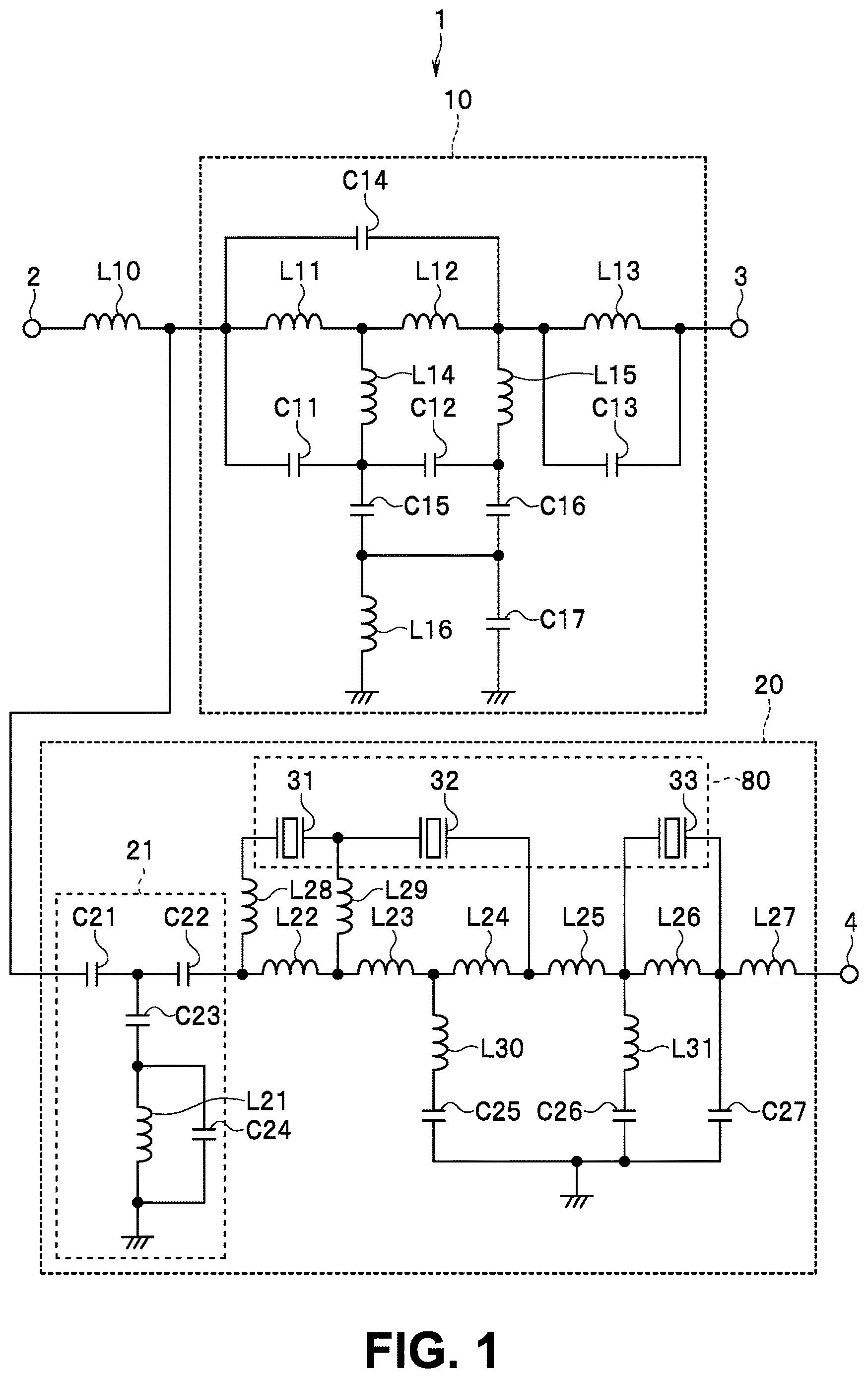
An embodiment of the present invention will be described below in detail with reference to the drawings. First, a schematic configuration of an electronic component 1 according to an embodiment of the present invention will be described with reference to . is a circuit diagram showing a circuit configuration of the electronic component 1 .
The electronic component 1 according to the present embodiment is a branching filter (diplexer) including a first filter 10 and a second filter 20 . The first filter 10 is configured to selectively pass a first signal of a frequency within a first passband. The second filter 20 is configured to selectively pass a second signal of a frequency within a second passband higher than the first passband.
The first filter 10 is an LC filter including at least one inductor and at least one capacitor. The second filter 20 is a filter, of so-called hybrid type, including at least one inductor, at least one capacitor, and at least one acoustic wave element. Examples of the at least one acoustic wave element may include a bulk acoustic wave element and a surface acoustic wave element.
The electronic component 1 further includes a common terminal 2 , a first signal terminal 3 , and a second signal terminal 4 . The first filter 10 is provided between the common terminal 2 and the first signal terminal 3 in the circuit configuration. The second filter 20 is provided between the common terminal 2 and the second signal terminal 4 in the circuit configuration. Note that, in the present application, the expression “in the (a) circuit configuration” is used to indicate not layout in physical configuration but layout in the circuit diagram.
Next, an example of a circuit configuration of the electronic component 1 will be described with reference to . The electronic component 1 further includes an inductor L 10 having one end connected to the common terminal 2 .
The first filter 10 includes a low-pass filter circuit including at least one inductor and at least one capacitor. In the example shown in , the first filter 10 includes inductors L 11 , L 12 , L 13 , L 14 , L 15 , and L 16 , and capacitors C 11 , C 12 , C 13 , C 14 , C 15 , C 16 , and C 17 .
One end of the inductor L 11 is connected to the other end of the inductor L 10 . One end of the inductor L 12 is connected to the other end of the inductor L 11 . One end of the inductor L 13 is connected to the other end of the inductor L 12 . The other end of the inductor L 13 is connected to the first signal terminal 3 .
One end of the inductor L 14 is connected to a connection point between the inductors L 11 and L 12 . One end of the inductor L 15 is connected to the other end of the inductor L 12 .
One end of the capacitor C 11 is connected to the one end of the inductor L 11 . The other end of the capacitor C 11 , one end of the capacitor C 12 , and one end of the capacitor C 15 are connected to the other end of the inductor L 14 . The other end of the capacitor C 12 and one end of the capacitor C 16 are connected to the other end of the inductor L 15 .
The capacitor C 13 is connected in parallel with the inductor L 13 . One end of the capacitor C 14 is connected to the one end of the inductor L 11 . The other end of the capacitor C 14 is connected to the other end of the inductor L 12 .
One end of the inductor L 16 is connected to the other end of the capacitor C 15 , and one end of the capacitor C 17 is connected to the other end of the capacitor C 16 . The other end of each of the inductor L 16 and the capacitor C 17 is connected to the ground.
The second filter 20 includes a circuit section including at least one inductor and at least one capacitor, at least one acoustic wave element, and a high-pass filter circuit 21 connected to the circuit section in series. In the example shown in , the high-pass filter circuit 21 includes an inductor L 21 , and capacitors C 21 , C 22 , C 23 , and C 24 .
One end of the capacitor C 21 is connected to the other end of the inductor L 10 . One end of the capacitor C 22 is connected to the other end of the capacitor C 21 . One end of the capacitor C 23 is connected to the connection point between the capacitors C 21 and C 22 .
One end of the inductor L 21 is connected to the other end of the capacitor C 23 . The other end of the inductor L 21 is connected to the ground. The capacitor C 24 is connected in parallel with the inductor L 21 .
In the example shown in , the at least one inductor in the circuit section of the second filter 20 is a plurality of inductors L 22 , L 23 , L 24 , L 25 , L 26 , and L 27 . The at least one capacitor in the circuit section of the second filter 20 is a plurality of capacitors C 25 , C 26 , and C 27 . The at least one acoustic wave element is a plurality of acoustic wave elements 31 , 32 , and 33 .
The circuit section of the second filter 20 further includes inductors L 28 , L 29 , L 30 , and L 31 . The circuit section of the second filter 20 is a circuit including the inductors L 22 to L 31 and the capacitors C 25 to C 27 , but excluding the high-pass filter circuit 21 and the acoustic wave elements 31 to 33 in the second filter 20 . The high-pass filter circuit 21 is provided between the common terminal 2 and the circuit section in the circuit configuration.
One end of the inductor L 22 is connected to the other end of the capacitor C 22 . One end of the inductor L 23 is connected to the other end of the inductor L 22 . One end of the inductor L 24 is connected to the other end of the inductor L 23 . One end of the inductor L 25 is connected to the other end of the inductor L 24 . One end of the inductor L 26 is connected to the other end of the inductor L 25 . One end of the inductor L 27 is connected to the other end of the inductor L 26 . The other end of the inductor L 27 is connected to the second signal terminal 4 .
One end of the inductor L 28 is connected to the one end of the inductor L 22 . One end of the inductor L 29 is connected to a connection point between the inductors L 22 and L 23 .
One end of the acoustic wave element 31 is connected to the other end of the inductor L 28 . The other end of the acoustic wave element 31 and one end of the acoustic wave element 32 is connected to the other end of the inductor L 29 . The other end of the acoustic wave element 32 is connected to a connection point between the inductors L 24 and L 25 . One end of the acoustic wave element 33 is connected to a connection point between the inductors L 25 and L 26 . The other end of the acoustic wave element 33 is connected to a connection point between the inductors L 26 and L 27 .
One end of the inductor L 30 is connected to a connection point between the inductors L 23 and L 24 . One end of the inductor L 31 is connected to the connection point between the inductors L 25 and L 26 .
One end of the capacitor C 25 is connected to the other end of the inductor L 30 . One end of the capacitor C 26 is connected to the other end of the inductor L 31 . One end of the capacitor C 27 is connected to the connection point between the inductors L 26 and L 27 . The other end of each of the capacitors C 25 to C 27 is connected to the ground.
The inductor L 22 is connected in parallel with the acoustic wave element 31 . The inductors L 23 and L 24 are connected in parallel with the acoustic wave element 32 . The inductor L 26 is connected in parallel with the acoustic wave element 33 .
The acoustic wave elements 31 to 33 are electrically connected in series. The inductors L 22 to L 27 are electrically connected in series. Note that an aspect in which two elements are electrically connected in series includes an aspect in which the two elements are connected in series via a conductor and an aspect in which the two elements are connected in series via an inductor. On the other hand, the aspect in which two elements are electrically connected in series does not include an aspect in which a conductor on a path connecting the two elements is interrupted, such as an aspect in which the two elements are connected to each other via a capacitor.
Each of the acoustic wave elements 31 to 33 , in a state of being electrically connected to the circuit section of the second filter 20 , is not electrically connected to the ground. In the present embodiment in particular, the conductors on the paths connecting both end of each of the acoustic wave elements 31 to 33 and the ground are interrupted by a capacitor.
Concerning the acoustic wave element 31 , in the second filter 20 , there are a first path and a second path, the first path connecting one end of the acoustic wave element 31 and the ground, the second path connecting the other end of the acoustic wave element 31 and the ground, the second path not via the same element(s) as those in the first path. The first path is a path via the high-pass filter circuit 21 . The conductor on the first path is interrupted by the capacitor C 22 . The conductor on the second path is interrupted by the capacitor C 25 , capacitor C 26 , or capacitor C 27 .
Concerning the acoustic wave element 32 , in the second filter 20 , there are a third path and a fourth path, the third path connecting one end of the acoustic wave element 32 and the ground, the fourth path connecting the other end of the acoustic wave element 32 and the ground, the fourth path not via the same element(s) as those in the third path. The third path may be a path via the inductors L 29 and L 22 and the high-pass filter circuit 21 in order or may be a path via the inductors L 29 , L 23 , and L 30 in order. The conductor on the former path is interrupted by the capacitor C 22 . The conductor on the latter path is interrupted by the capacitor C 25 .
As long as the condition that the fourth path is not via the same element(s) as those in the third path is satisfied, the fourth path may be a path via the inductors L 24 and L 30 in order or may be a path via the inductor L 25 . The conductor on the former path is interrupted by capacitor C 25 . The conductor on the latter path is interrupted by the capacitor C 26 or capacitor C 27 .
Concerning the acoustic wave element 33 , in the second filter 20 , there are a fifth path and a sixth path, the fifth path connecting one end of the acoustic wave element 33 and the ground, the sixth path connecting the other end of the acoustic wave element 33 and the ground, the sixth path not via the same element(s) as those in the fifth path. The fifth path is a path via the capacitor C 27 . The conductor on the fifth path is interrupted by the capacitor C 27 . The conductor on the sixth path is interrupted by the capacitor C 22 , capacitor C 25 , or capacitor C 26 .
Next, other configurations of the electronic component 1 will be described with reference to to 4 . is a perspective view showing the electronic component 1 . are each a perspective view showing a first main body.
The electronic component 1 includes a first main body 50 including a plurality of dielectric layers stacked together, a second main body 80 mounted on the first main body 50 , and a sealing part 90 sealing the first main body 50 and the second main body 80 . The sealing part 90 is formed of a resin, for example.
The first main body 50 includes the common terminal 2 , the first signal terminal 3 , the second signal terminal 4 , the first filter 10 , the high-pass filter circuit 21 of the second filter 20 , and the circuit section of the second filter 20 .
The second main body 80 includes at least one acoustic wave element that is electrically connected to the circuit section of the second filter 20 and that is connected in parallel with at least one inductor in the circuit section of the second filter 20 . In the present embodiment in particular, the second main body 80 includes the acoustic wave elements 31 to 33 .
The first main body 50 includes a first surface 50 A and a second surface 50 B located at opposite ends in the stacking direction T of the plurality of dielectric layers, and four side surfaces 50 C to 50 F connecting the first surface 50 A and the second surface 50 B. The side surfaces 50 C and 50 D are opposite to each other, and also the side surfaces 50 E and 50 F are opposite to each other. The side surfaces 50 C to 50 F each are perpendicular to both of the first surface 50 A and the second surface 50 B.
Here, an X direction, a Y direction, and a Z direction will be defined as shown in to 4 . The X direction, the Y direction, and the Z direction are orthogonal to one another. In the present embodiment, one direction parallel to the stacking direction is referred to as the Z direction. The Z direction is also one direction parallel to a direction in which the first main body 50 and the second main body 80 are arranged. The opposite directions to the X, Y, and Z directions are defined as −X, −Y, and −Z directions, respectively. The expression “when seen in the stacking direction T” means that an object is viewed from a position away in the Z or −Z direction.
As shown in , the first surface 50 A is located at an end of the first main body 50 in the Z direction. The first surface 50 A is located at an end of the first main body 50 in the −Z direction. The first surface 50 A is also a bottom surface of the first main body 50 . The second surface 50 B is located at an end of the first main body 50 in the Z direction. The second surface 50 B is also a top surface of the first main body 50 and is also a mounting surface for the second main body 80 to be mounted on. shows the first main body 50 in a view from the second surface 50 B side. shows the first main body 50 in a view from the first surface 50 A side.
The side surface 50 C is located at an end of the first main body 50 in the −X direction. The side surface 50 D is located at an end of the first main body 50 in the X direction. The side surface 50 E is located at an end of the first main body 50 in the −Y direction. The side surface 50 F is located at an end of the first main body 50 in the Y direction.
The first main body 50 further includes a plurality of electrodes 111 , 112 , 113 , 114 , 115 , and 116 provided on the first surface 50 A of the first main body 50 . The electrodes 111 , 112 , and 113 are arranged in this order in the X direction at positions closer to the side surface 50 E than to the side surface 50 F. The electrodes 114 , 115 , and 116 are arranged in this order in the −X direction at positions closer to the side surface 50 F than to the side surface 50 E.
The electrode 112 corresponds to the common terminal 2 . The electrode 114 corresponds to the first signal terminal 3 . The electrode 116 corresponds to the second signal terminal 4 . Accordingly, the common terminal 2 , the first signal terminal 3 , and the second signal terminal 4 are provided on the first surface 50 A of the first main body 50 . Each of the electrodes 111 , 113 , and 115 is connected to the ground.
The first main body 50 further includes a plurality of electrodes 121 , 122 , 123 , 124 , 125 , 126 , 127 , 128 , and 129 provided on the second surface 50 B of the first main body 50 . The plurality of electrodes 121 to 129 are used for electrical connection between the first main body 50 and the second main body 80 . The electrodes 121 , 122 , and 123 are arranged in this order in the X direction at positions closer to the side surface 50 E than to the side surface 50 F. The electrodes 125 , 126 , and 127 are arranged in this order in the −X direction at positions closer to the side surface 50 F than to the side surface 50 E. The electrode 124 is arranged between the electrodes 123 and 125 . The electrode 128 is arranged between the electrodes 121 and 127 . The electrode 129 is arranged between the electrodes 122 and 126 .
The second main body 80 is mounted on the second surface 50 B of the first main body 50 . The second main body 80 includes a plurality of electrodes (not illustrated) each electrically connected to one of the acoustic wave elements 31 to 33 . In a state that the second main body 80 is mounted on the first main body 50 , a plurality of electrodes of the second main body 80 faces the electrodes 121 to 129 of the first main body 50 . Each of the plurality of electrodes of the second main body 80 is physically connected to one of the electrodes 121 to 129 by, for example, a solder bump (not illustrated).
Next, an example of the plurality of dielectric layers, the plurality of conductor layers, and the plurality of through holes constituting the first main body 50 will be described with reference to A to 12 . In this example, the first main body 50 includes twenty one dielectric layers stacked together. The twenty one dielectric layers are hereinafter referred to as first to twenty-first dielectric layers in the order from bottom to top. The first to twenty-first dielectric layers are denoted by reference numerals 51 to 71 , respectively.
In A to 12 , a plurality of circles represent a plurality of through holes. Each of the dielectric layers 51 to 71 has a plurality of through holes formed. Each of the plurality of through holes is formed by filling a hole intended for a through hole with a conductive paste. Each of the plurality of through holes is connected to a terminal, a conductor layer, or another through hole.
In A to 12 , a plurality of specific through holes out of the plurality of through holes are denoted by reference numerals. Regarding the connection relation between each of the plurality of specific through holes and a terminal, a conductor layer, or another through hole, a connection relation in a state that the first to twenty-first dielectric layers 51 to 71 are stacked together is described.
A shows a patterned surface of the first dielectric layer 51 . The electrodes 111 to 116 are formed on the patterned surface of the dielectric layer 51 . In A , through holes denoted by reference numerals 51 T 1 and 51 T 2 are connected to the electrodes 111 and 115 , respectively. Note that, in the following description, the through hole denoted by the reference numeral 51 T 1 is simply referred to as a through hole 51 T 1 . Such manner for through hole 51 T 1 similarly applies to through holes denoted by reference numerals other than the through hole 51 T 1 .
B shows a patterned surface of the second dielectric layer 52 . Conductor layers 521 and 522 intended for inductors, and a conductor layer 523 are formed on the patterned surface of the dielectric layer 52 . Through holes 52 T 1 and 52 T 2 shown in B , and the through holes 51 T 1 and 51 T 2 formed in the dielectric layer 51 are connected to the conductor layer 523 .
C shows a patterned surface of the third dielectric layer 53 . A conductor layer 531 intended for an inductor, and conductor layers 532 , 533 , 534 , 535 , and 536 are formed on the patterned surface of the dielectric layer 53 . A through hole 53 T 1 shown in C , and the through holes 52 T 1 and 52 T 2 formed in the dielectric layer 52 are connected to the conductor layer 536 .
A shows a patterned surface of the fourth dielectric layer 54 . Conductor layers 541 and 542 intended for inductors, and conductor layers 543 , 544 , 545 , 546 and 547 are formed on the patterned surface of the dielectric layer 54 . A through hole 54 T 1 shown in A is connected to the through hole 53 T 1 formed in the dielectric layer 53 .
B shows a patterned surface of the fifth dielectric layer 55 . Conductor layers 551 and 552 intended for inductors, and conductor layers 553 , 554 , 555 , 556 , 557 , 558 , and 559 are formed on the patterned surface of the dielectric layer 55 . A through hole 55 T 1 shown in B is connected to the through hole 54 T 1 formed in the dielectric layer 54 .
C shows a patterned surface of the sixth dielectric layer 56 . A conductor layer 561 is formed on the patterned surface of the dielectric layer 56 . A through hole 56 T 1 shown in C is connected to the through hole 55 T 1 formed in the dielectric layer 55 .
A shows a patterned surface of the seventh dielectric layer 57 . A conductor layer 571 is formed on the patterned surface of the dielectric layer 57 . A through hole 57 T 1 shown in A and the through hole 56 T 1 formed in the dielectric layer 56 are connected to the conductor layer 571 .
B shows a patterned surface of the eighth dielectric layer 58 . A through hole 58 T 1 shown in B is connected to the through hole 57 T 1 formed in the dielectric layer 57 .
C shows a patterned surface of the ninth dielectric layer 59 . A conductor layer 591 intended for an inductor is formed on the patterned surface of the dielectric layer 59 . A through hole 59 T 1 shown in C is connected to the through hole 58 T 1 formed in the dielectric layer 58 .
A shows a patterned surface of the tenth dielectric layer 60 . Conductor layers 601 , 602 , 603 , and 604 intended for inductors are formed on the patterned surface of the dielectric layer 60 . The conductor layer 603 is connected to the conductor layer 602 . A through hole 60 T 1 shown in A is connected to the through hole 59 T 1 formed in the dielectric layer 59 .
B shows a patterned surface of the eleventh dielectric layer 61 . Conductor layers 611 , 612 , and 613 intended for inductors are formed on the patterned surface of the dielectric layer 61 . The conductor layer 613 is connected to the conductor layer 612 . A through hole 61 T 1 shown in B is connected to the through hole 60 T 1 formed in the dielectric layer 60 .
C shows a patterned surface of the twelfth dielectric layer 62 . A through hole 62 T 1 shown in C is connected to the through hole 61 T 1 formed in the dielectric layer 61 .
A shows a patterned surface of the thirteenth dielectric layer 63 . A conductor layer 631 is formed on the patterned surface of the dielectric layer 63 . A through hole 63 T 1 shown in A and the through hole 62 T 1 formed in the dielectric layer 62 are connected to the conductor layer 631 .
B shows a patterned surface of the fourteenth dielectric layer 64 . Conductor layers 641 , 642 , and 643 intended for inductors are formed on the patterned surface of the dielectric layer 64 . A through hole 64 T 1 shown in B is connected to the through hole 63 T 1 formed in the dielectric layer 63 .
C shows a patterned surface of the fifteenth dielectric layer 65 . Conductor layers 651 , 652 , and 653 intended for inductors are formed on the patterned surface of the dielectric layer 65 . A through hole 65 T 1 shown in C is connected to the through hole 64 T 1 formed in the dielectric layer 64 .
A shows a patterned surface of the sixteenth dielectric layer 66 . A through hole 66 T 1 shown in A is connected to the through hole 65 T 1 formed in the dielectric layer 65 .
B shows a patterned surface of the seventeenth dielectric layer 67 . A conductor layer 671 intended for an inductor is formed on the patterned surface of the dielectric layer 67 . A through hole 67 T 1 shown in B is connected to the through hole 66 T 1 formed in the dielectric layer 66 .
C shows a patterned surface of the eighteenth dielectric layer 68 . A conductor layer 681 intended for an inductor is formed on the patterned surface of the dielectric layer 68 . A through hole 68 T 1 shown in C is connected to the through hole 67 T 1 formed in the dielectric layer 67 .
A shows a patterned surface of the nineteenth dielectric layer 69 . Conductor layers 691 , 692 , 693 , 694 , 695 , 696 , 697 , and 698 intended for inductors are formed on the patterned surface of the dielectric layer 69 . A through hole 69 T 1 shown in A is connected to the through hole 68 T 1 formed in the dielectric layer 68 .
B shows a patterned surface of the twentieth dielectric layer 70 . Conductor layers 701 , 702 , 703 , 704 , 705 , 706 , 707 , and 708 intended for inductors are formed on the patterned surface of the dielectric layer 70 . A through hole 70 T 1 shown in B is connected to the through hole 69 T 1 formed in the dielectric layer 69 .
C shows a patterned surface of the twenty-first dielectric layer 71 . Conductor layers 711 , 712 , 713 , 714 , 715 , and 716 are formed on the patterned surface of the dielectric layer 71 . Through holes 71 T 1 , 71 T 2 , and 71 T 3 shown in C , and the through hole 70 T 1 formed in the dielectric layer 70 are connected to the conductor layer 711 .
shows a surface of the twenty-first dielectric layer 71 opposite to the patterned surface thereof. The surface of the dielectric layer 71 opposite to the patterned surface thereof is hereinafter referred to as an electrode formation surface of the dielectric layer 71 . The electrodes 121 , 122 , 123 , 124 , 125 , 126 , 127 , 128 , and 129 are formed on the electrode formation surface of the dielectric layer 71 . The through holes 71 T 1 , 71 T 2 , and 71 T 3 formed in the dielectric layer 71 are connected to the electrodes 122 , 126 , and 129 , respectively.
The first main body 50 includes the first to twenty-first dielectric layers 51 to 71 stacked together such that the patterned surface of the first dielectric layer 51 serves as the first surface 50 A of the first main body 50 and the electrode formation surface of the twenty-first dielectric layer 71 serves as the second surface 50 B of the first main body 50 .
Each of the plurality of through holes shown in A to 12 is connected to a conductor layer overlapping with in the stacking direction T or to another through hole overlapping with in the stacking direction T, when the first to twenty-first dielectric layers 51 to 71 are stacked together. Of the plurality of through holes shown in A to 12 , a through hole located within an electrode or a conductor layer is connected to the electrode or the conductor layer.
shows inside of the first main body 50 including the first to twenty-first dielectric layers 51 to 71 stacked together. As shown in , the plurality of conductor layers and the plurality of through holes shown in A to 12 are stacked together inside the first main body 50 .
Correspondences between the components of the circuit of the electronic component 1 shown in and the components inside the first main body 50 shown in A to 12 will be described below. First, the inductor L 10 will be described. The inductor L 10 includes the conductor layers 601 , 611 , 691 , and 701 intended for inductors, a plurality of through holes including one connecting a pair of the conductor layers 601 and 611 , one connecting a pair of the conductor layers 611 and 691 , and one connecting a pair of the conductor layers 691 and 701 , and a plurality of through holes connecting the conductor layer 691 and the conductor layer 547 .
Next, the first filter 10 will be described. The inductor L 11 includes the conductor layers 641 , 651 , 692 , and 702 intended for inductors, and a plurality of through holes including one connecting a pair of the conductor layers 641 and 651 , one connecting a pair of the conductor layers 651 and 692 , and one connecting a pair of the conductor layers 692 and 702 .
The inductor L 12 includes the conductor layers 693 and 703 intended for an inductor, a plurality of through holes connecting the conductor layers 693 and 703 , a plurality of through holes connecting the conductor layers 693 and 554 , and a plurality of through holes connecting the conductor layers 693 and 559 .
The inductor L 13 includes the conductor layers 694 and 704 intended for an inductor, a plurality of through holes connecting the conductor layers 694 and 704 , a plurality of through holes connecting the conductor layers 694 and 554 , and a plurality of through holes connecting the conductor layers 694 and 559 .
The inductor L 14 includes a part of each of the conductor layers 543 and 554 . The inductor L 15 includes a part of the conductor layer 544 . The inductor L 16 includes the conductor layer 521 intended for an inductor.
The capacitor C 11 includes the conductor layers 543 and 553 , and the dielectric layer 54 interposed between these conductor layers. The capacitor C 12 includes the conductor layers 532 , 544 , and 554 , and the dielectric layers 53 and 54 each interposed between these conductor layers. The capacitor C 13 includes the conductor layers 533 and 544 , and the dielectric layer 53 interposed between these conductor layers.
The capacitor C 14 includes the conductor layers 555 and 561 , and the dielectric layer 55 interposed between these conductor layers. The capacitor C 15 includes the conductor layers 534 and 543 , and the dielectric layer 53 interposed between these conductor layers. The capacitor C 16 includes the conductor layers 534 and 544 , and the dielectric layer 53 interposed between these conductor layers. The capacitor C 17 is floating capacitance generated between the electrode 113 and the conductor layer 534 .
Next, the high-pass filter circuit 21 of the second filter 20 will be described. The inductor L 21 includes the conductor layers 522 , 531 , 541 , 542 , 551 , 552 , 695 , 696 , 697 , 705 , 706 , and 707 intended for inductors, a plurality of through holes including one connecting a pair of the conductor layers 522 and 531 , one connecting a pair of the conductor layers 541 and 551 , one connecting a pair of the conductor layers 542 and 552 , one connecting a pair of the conductor layers 695 and 705 , one connecting a pair of the conductor layers 696 and 706 , one connecting a pair of the conductor layers 697 and 707 , one connecting a pair of the conductor layers 551 and 695 , one connecting a pair of the conductor layers 551 and 696 , one connecting a pair of the conductor layers 552 and 696 , one connecting a pair of the conductor layers 552 and 697 , and one connecting a pair of the conductor layers 531 and 697 , and a plurality of through holes connecting the conductor layer 695 and the conductor layer 557 .
The capacitor C 21 includes the conductor layers 535 and 545 , and the dielectric layer 53 interposed between these conductor layers. The capacitor C 22 includes the conductor layers 545 and 556 , and the dielectric layer 54 interposed between these conductor layers. The capacitor C 23 includes the conductor layers 545 and 557 , and the dielectric layer 54 interposed between these conductor layers.
The capacitor C 24 corresponds to a total of floating capacitance generated between the conductor layers 551 and 557 , floating capacitance generated between the conductor layers 695 and 696 , and floating capacitance generated between the conductor layers 705 and 706 .
Next, a part other than the high-pass filter circuit 21 of the second filter 20 will be described. The acoustic wave element 31 is provided between the electrodes 123 and 124 . The acoustic wave element 32 is provided between the electrodes 124 and 125 . The acoustic wave element 33 is provided between the electrodes 121 and 128 .
The inductor L 22 includes the conductor layers 602 and 612 intended for an inductor and a plurality of through holes connecting the conductor layer 602 and the conductor layer 612 . The inductor L 23 includes the conductor layers 603 and 613 intended for an inductor and a plurality of through holes connecting the conductor layer 602 and the conductor layer 612 . The inductor L 24 includes the conductor layers 642 and 652 intended for an inductor and a plurality of through holes connecting the conductor layer 642 and the conductor layer 652 .
The inductor L 25 includes the conductor layers 698 and 708 intended for an inductor and a plurality of through holes connecting the conductor layer 698 and the conductor layer 708 . The inductor L 26 includes the conductor layers 591 and 604 intended for an inductor and a plurality of through holes connecting the conductor layer 591 and the conductor layer 604 . The inductor L 27 includes the conductor layers 643 and 653 intended for an inductor and a plurality of through holes connecting the conductor layer 643 and the conductor layer 653 .
The inductor L 28 includes the conductor layers 671 and 681 intended for an inductor and a plurality of through holes connecting the conductor layer 671 and the conductor layer 681 . The inductor L 29 includes a plurality of through holes connecting the conductor layers 612 and 613 and the conductor layer 714 , and one through hole connecting the conductor layer 714 and the electrode 124 .
The inductor L 30 includes a plurality of through holes connecting the conductor layer 546 and the conductor layer 603 . The inductor L 31 includes a plurality of through holes connecting the conductor layer 558 and the conductor layer 698 .
The capacitor C 25 includes the conductor layers 523 and 536 , and the dielectric layer 52 interposed between these conductor layers. The capacitor C 26 includes the conductor layers 536 and 558 , and the dielectric layers 53 and 54 each interposed between these conductor layers. The capacitor C 27 includes the electrode 116 , the conductor layer 522 , and the dielectric layer 51 interposed between the electrode 116 and the conductor layer 522 .
Next, structural features of the electronic component 1 according to the present embodiment will be described with reference to to 16 . is a plan view showing a part of inside of the first main body 50 . are each a perspective view showing a part of inside of the first main body 50 .
The inductor L 11 is an inductor wound about an axis extending in a direction parallel to the stacking direction T. In other words, each of the conductor layers 641 , 651 , 692 , and 702 constituting the inductor L 11 is wound about an axis extending in the direction parallel to the stacking direction T.
Each of the inductors L 10 , L 12 , L 13 , and L 21 is an inductor of conductor structure type wound about an axis extending in a direction orthogonal to the stacking direction T. Here, a columnar structure including a plurality of through holes connected in series is referred to as a columnar conductor. The columnar conductor extends in the direction parallel to the stacking direction T. The inductor of conductor structure type includes at least one conductor layer and a plurality of columnar conductors.
Each of the inductors L 10 , L 12 , L 13 , and L 21 is also a winding having a rectangular shape or substantially rectangular shape. For the winding having the rectangular shape or substantially rectangular shape, when the winding is considered to be a rectangle, the number of times of winding may be ¼ times per one side of the rectangle.
The number of times of winding for the inductor L 10 is one time. As shown in , the inductor L 10 includes a conductor layer part L 10 a 1 , a columnar conductor L 10 b 1 connected to the conductor layer part L 10 a 1 , a conductor layer part L 10 a 2 connected to the columnar conductor L 10 b 1 , and a columnar conductor L 10 b 2 connected to the conductor layer part L 10 a 2 . The conductor layer part L 10 a 1 includes the conductor layers 601 and 611 . The conductor layer part L 10 a 2 includes the conductor layers 691 and 701 .
The number of times of winding for the inductor L 12 is ¾ times. As shown in , the inductor L 12 includes three columnar conductors L 12 b 1 , a conductor layer part L 12 a connected to the three columnar conductors L 12 b 1 , and three columnar conductors L 12 b 2 connected to the conductor layer part L 12 a . The conductor layer part L 12 a includes the conductor layers 693 and 703 .
The number of times of winding for the inductor L 13 is ¾ times. As shown in , the inductor L 13 includes a columnar conductor L 13 b 1 , a conductor layer part L 13 a connected to the columnar conductor L 13 b 1 , and a columnar conductor L 13 b 2 connected to the conductor layer part L 13 a . The conductor layer part L 13 a includes the conductor layers 694 and 704 .
The number of times of winding for the inductor L 21 is three times. As shown in , the inductor L 21 includes a columnar conductor L 21 b 1 , a conductor layer part L 21 a 1 connected to the columnar conductor L 21 b 1 , a columnar conductor L 21 b 2 connected to the conductor layer part L 21 a 1 , a conductor layer part L 21 a 2 connected to the columnar conductor L 21 b 2 , a columnar conductor L 21 b 3 connected to the conductor layer part L 21 a 2 , a conductor layer part L 21 a 3 connected to the columnar conductor L 21 b 3 , a columnar conductor L 21 b 4 connected to the conductor layer part L 21 a 3 , a conductor layer part L 21 a 4 connected to the columnar conductor L 21 b 4 , a columnar conductor L 21 b 5 connected to the conductor layer part L 21 a 4 , a conductor layer part L 21 a 5 connected to the columnar conductor L 21 b 5 , a columnar conductor L 21 b 6 connected to the conductor layer part L 21 a 5 , and a conductor layer part L 21 a 6 connected to the columnar conductor L 21 b 6 .
The conductor layer part L 21 a 1 includes the conductor layers 695 and 705 . The conductor layer part L 21 a 2 includes the conductor layers 541 and 551 . The conductor layer part L 21 a 3 includes the conductor layers 696 and 706 . The conductor layer part L 21 a 4 includes the conductor layers 542 and 552 . The conductor layer part L 21 a 5 includes the conductor layers 697 and 707 . The conductor layer part L 21 a 6 includes the conductor layers 522 and 532 .
Next, concerning the inductors L 10 , L 12 , L 13 , and L 21 of conductor structure type, structural features of the electronic component 1 according to the present embodiment will be described further in detail. The first main body 50 includes the common terminal 2 , the first signal terminal 3 , the second signal terminal 4 , and the inductors L 10 , L 12 , L 13 , and L 21 . The inductors L 10 , L 12 , L 13 , and L 21 are integrated with the first main body 50 . The inductor L 10 is provided between the common terminal 2 and the first and second signal terminals 3 and 4 , in the circuit configuration. The inductors L 12 and L 13 are provided between the common terminal 2 and the first signal terminal 3 , in the circuit configuration. The inductor L 21 is provided between the common terminal 2 and the second signal terminal 4 , in the circuit configuration.
The second main body 80 includes the acoustic wave elements 31 to 33 . The acoustic wave elements 31 to 33 are provided between the common terminal 2 and the second signal terminal 4 , in the circuit configuration.
In , a region surrounded by a dashed line denoted by a reference numeral R 80 shows a mounting region for the second main body 80 to be mounted on. The second surface 50 B of the first main body 50 includes the mounting region R 80 . The electrodes 121 to 129 provided on the second surface 50 B are arranged within the mounting region R 80 . A planar shape of the second main body 80 (shape when seen in the stacking direction T) may be the same as the shape of the mounting region R 80 . Alternatively, the second main body 80 may include a first part having a planar shape the same as that of the mounting region R 80 and a second part having a planar shape larger than the shape of the mounting region R 80 . In this case, the second main body 80 is mounted on the first main body 50 , in a posture where the first part is located between the first main body 50 and the second part.
In a state that the second main body 80 is mounted on the first main body 50 , the inductors L 10 , L 12 , L 13 , and L 21 are arranged surrounding at least a part of the second main body 80 , when seen in the stacking direction T. In the present embodiment in particular, a plurality of components of the inductors L 10 , L 12 , L 13 , and L 21 except the conductor layer part L 10 a 1 of the inductor L 10 are arranged surrounding the mounting region R 80 , when seen in the stacking direction T. In other words, the entirety of each of the inductors L 12 , L 13 , and L 21 is not overlapping with the mounting region R 80 , when seen in the stacking direction T. A plurality of columnar conductors included in each of the inductors L 10 , L 12 , L 13 , and L 21 are not overlapping with the mounting region R 80 , when seen in the stacking direction T. In contrast, a part of the conductor layer part L 10 a 1 of the inductor L 10 is overlapping with the mounting region R 80 , when seen in the stacking direction T. Accordingly, in the present embodiment, the inductors L 10 , L 12 , L 13 , and L 21 are arranged surrounding a part of the second main body 80 , when seen in the stacking direction T.
As shown in , the conductor layer part L 10 a 2 (conductor layers 691 and 701 ) of the inductor L 10 is arranged between the mounting region R 80 and the side surface 50 E and extends along the side surface 50 E, when seen in the stacking direction T. In the present embodiment in particular, the conductor layer part L 10 a 2 mostly extends in a direction parallel to the X direction. No conductor is provided between the conductor layer part L 10 a 2 and the side surface 50 E.
As shown in , the conductor layer part L 12 a (conductor layers 693 and 703 ) of the inductor L 12 is arranged between the mounting region R 80 and the side surface 50 D and extends along the side surface 50 D, when seen in the stacking direction T. In the present embodiment in particular, the conductor layer part L 12 a mostly extends in a direction parallel to the Y direction. No conductor is provided between the conductor layer part L 12 a (conductor layers 693 and 703 ) and the side surface 50 D.
As shown in , the conductor layer part L 13 a (conductor layers 694 and 704 ) of the inductor L 13 is arranged between the mounting region R 80 and the side surface 50 F and extends in the direction parallel to the X direction along the side surface 50 F, when seen in the stacking direction T. In the present embodiment in particular, the conductor layer part L 13 a mostly extends in the direction parallel to the X direction. No conductor is provided between the conductor layer part L 13 a and the side surface 50 F.
As shown in , each of the conductor layer part L 21 a 1 (conductor layers 695 and 705 ) and the conductor layer part L 21 a 3 (conductor layers 696 and 706 ) of the inductor L 21 is arranged between the mounting region R 80 and the side surface 50 C and extending along the side surface 50 C, when seen in the stacking direction T. In the present embodiment in particular, each of the conductor layer parts L 21 a 1 and L 21 a 3 mostly extends in the direction parallel to the Y direction. No conductor is provided between the conductor layer part L 21 a 1 and the side surface 50 C. The conductor layer part L 21 a 3 is arranged at a position where the conductor layer part L 21 a 3 and the side surface 50 C sandwiches the conductor layer part L 21 a 1 .
As shown in , the conductor layer part L 21 a 5 (conductor layers 697 and 707 ) of the inductor L 21 is arranged between the mounting region R 80 and the side surface 50 F and extends along the side surface 50 F, when seen in the stacking direction T. In the present embodiment in particular, the conductor layer part L 21 a 5 mostly extends in the direction parallel to the X direction. No conductor is provided between the conductor layer part L 21 a 5 and the side surface 50 F.
The conductor layer part L 21 a 2 (conductor layers 541 and 551 ) of the inductor L 21 shown in is arranged between the mounting region R 80 and the side surface 50 C and extending along the side surface 50 C, when seen in the stacking direction T. In the present embodiment in particular, the conductor layer part L 21 a 2 mostly extends in the direction parallel to the Y direction.
Each of the conductor layer part L 21 a 4 (conductor layers 542 and 552 ) and the conductor layer part L 21 a 6 (conductor layers 522 and 532 ) of the inductor L 21 shown in is arranged between the mounting region R 80 and the side surface 50 F and extends along the side surface 50 F, when seen in the stacking direction T. In the present embodiment in particular, each of the conductor layer parts L 21 a 4 and L 21 a 6 mostly extends in the direction parallel to the X direction. No conductor is provided between the conductor layer part L 21 a 6 and the side surface 50 F. The conductor layer part L 21 a 4 is arranged at a position where the conductor layer part L 21 a 4 and the side surface 50 F sandwiches the conductor layer part L 21 a 6 , when seen in the stacking direction T.
The first main body 50 further includes the first filter 10 provided between the common terminal 2 and the first signal terminal 3 in the circuit configuration and the second filter 20 that is provided between the common terminal 2 and the second signal terminal 4 in the circuit configuration and that includes the acoustic wave elements 31 to 33 . The first filter 10 includes the inductors L 12 and L 13 of conductor structure type. The second filter includes the inductor L 21 of conductor structure type.
In a state that the second main body 80 is mounted on the first main body 50 , the second main body 80 overlaps with a part of the second filter 20 , when seen in the stacking direction T. The second filter 20 includes the inductor L 21 not overlapping with the second main body 80 when seen in the stacking direction T and the inductors L 22 to L 31 overlapping with the second main body 80 when seen in the stacking direction T. As shown in , in the circuit configuration, the inductor L 21 is provided at a position further from the acoustic wave elements 31 to 33 than the inductors L 22 to L 31 .
Each of the inductors L 22 to L 29 is a planar inductor extending along a plane intersecting with the stacking direction T. The planar inductor is an inductor that has no columnar conductor as a component, the inductor not wound about an axis extending in a direction orthogonal to the stacking direction T. The planar inductor may be or may not be wound about an axis extending in the direction parallel to the stacking direction T.
The inductor L 10 includes the conductor layer 701 closest to the second surface 50 B, in other words, the second main body 80 . The inductor L 12 includes the conductor layer 703 closest to the second surface 50 B. The inductor L 13 includes the conductor layer 704 closest to the second surface 50 B. The inductor L 21 includes the conductor layers 705 to 707 closest to the second surface 50 B. Each of the inductors L 22 to L 29 is arranged at a position further from the second surface 50 B, in other words, the second main body 80 , than the conductor layers 701 and 703 to 707 .
Each of the inductors L 30 and L 31 is a columnar inductor extending along the stacking direction T. The columnar inductor is an inductor that has a columnar conductor as a component and that has no conductor layer as a component, the inductor not wound about an axis extending in a direction orthogonal to the stacking direction T.
Next, features of the inductor L 21 will be described in detail with reference to . As described above, the inductor L 21 includes the columnar conductors L 21 b 1 to L 21 b 6 . The columnar conductors L 21 b 1 and L 21 b 3 are adjacent to each other. Currents in the columnar conductors L 21 b 1 and L 21 b 3 flow in the same direction. Specifically, each of the columnar conductors L 21 b 1 and L 21 b 3 includes a first end portion closest to the first surface 50 A and a second end portion closest to the second surface 50 B. The first end portion of the columnar conductor L 21 b 1 is, in the circuit configuration, at a position further from the ground than the second end portion of the columnar conductor L 21 b 1 . The first end portion of the columnar conductor L 21 b 3 is, in the circuit configuration, at a position further from the ground than the second end portion of the columnar conductor L 21 b 3 .
The columnar conductors L 21 b 2 , L 21 b 4 , and L 21 b 6 are adjacent to each other. Currents in the columnar conductors L 21 b 2 , L 21 b 4 , and L 21 b 6 flow in the same direction. Specifically, each of the columnar conductors L 21 b 2 , L 21 b 4 , and L 21 b 6 includes a first end portion closest to the first surface 50 A and a second end portion closest to the second surface 50 B. The first end portion of the columnar conductor L 21 b 2 is, in the circuit configuration, at a position closer to the ground than the second end portion of the columnar conductor L 21 b 2 . The first end portion of the columnar conductor L 21 b 4 is, in the circuit configuration, at a position closer to the ground than the second end portion of the columnar conductor L 21 b 4 . The first end portion of the columnar conductor L 21 b 6 is, in the circuit configuration, at a position closer to the ground than the second end portion of the columnar conductor L 21 b 6 .
The inductor L 21 further includes the conductor layer 695 connected to the second end portion of each of the columnar conductors L 21 b 1 and L 21 b 2 , the conductor layer 696 connected to the second end portion of each of the columnar conductors L 21 b 3 and L 21 b 4 , and the conductor layer 697 connected to the second end portion of each of the columnar conductors L 21 b 5 and L 21 b 6 . A longitudinal direction of the conductor layer 695 and a longitudinal direction of the conductor layer 697 are intersecting with each other. An angle formed by the longitudinal direction of the conductor layer 695 and the longitudinal direction of the conductor layer 697 is preferably at an angle of 70° or more and 110° or less, in a viewpoint such that each of the conductor layers 695 and 697 does not overlap with the mounting region R 80 when seen in the stacking direction T and for the mounting region R 80 to have a large area.
The conductor layer 696 is arranged at a position where the conductor layer 696 and the side surface 50 C sandwich the conductor layer 695 . In the present embodiment in particular, the longitudinal direction of the conductor layer 695 and the longitudinal direction of the conductor layer 696 are parallel to or substantially parallel to each other. The longitudinal direction of the conductor layer 696 and the longitudinal direction of the conductor layer 697 are intersecting with each other. An angle formed by the longitudinal direction of the conductor layer 696 and the longitudinal direction of the conductor layer 697 is preferably 70° or more and 110° or less.
The shape and arrangement of the conductor layers 705 , 706 , and 707 are the same or substantially the same as the shape and arrangement of the conductor layers 695 , 696 , and 697 , respectively, except the position in the stacking direction T. The above description on the conductor layers 695 , 696 , and 697 also applies to the conductor layers 705 , 706 , and 707 .
Next, other features of the electronic component 1 according to the present embodiment will be described with reference to . shows the conductor layers 523 , 536 , 571 , 631 , and 711 , and the through holes 51 T 1 , 51 T 2 , 52 T 1 , 52 T 2 , 53 T 1 , 54 T 1 , 55 T 1 , 56 T 1 , 57 T 1 , 58 T 1 , 59 T 1 , 60 T 1 , 61 T 1 , 62 T 1 , 63 T 1 , 64 T 1 , 65 T 1 , 66 T 1 , 67 T 1 , 68 T 1 , 69 T 1 , 70 T 1 , and 72 T 1 to 72 T 3 . These conductor layers and through holes are electrically connected to each other, constituting a ground conductor.
The ground conductor electrically connects the electrodes 122 , 126 , and 129 among the electrodes 121 to 129 used for electrical connection between the first main body 50 and the second main body 80 to the electrodes 111 and 115 connected to the ground. In the first main body 50 , the ground conductor is provided passing between a plurality of conductors constituting the first filter 10 and a plurality of conductors constituting the second filter 20 .
Next, an example of characteristics of the electronic component 1 according to the present embodiment will be described. is a characteristic chart showing the pass attenuation characteristics of the electronic component 1 . In , the horizontal axis indicates frequency and the vertical axis indicates attenuation. In , a curve denoted by a reference numeral 91 indicates a pass attenuation characteristic between the common terminal 2 and the first signal terminal 3 , in other words, a pass attenuation characteristic of the first filter 10 . In , a curve denoted by a reference numeral 92 indicates a pass attenuation characteristic between the common terminal 2 and the second signal terminal 4 , in other words, a pass attenuation characteristic of the second filter 20 .
Now, the operation and effects of the electronic component 1 according to the present embodiment will be described. In the present embodiment, the first main body 50 includes the first filter 10 and the second filter 20 , and the second main body 80 includes the acoustic wave elements 31 to 33 .
Here, it is considered that a second main body of a comparative example including an acoustic wave element having one end connected to the ground is mounted on the first main body 50 . In this case, the acoustic wave element is connected, via inside of the first main body 50 , to an electrode that is provided on the first surface 50 A of the first main body 50 and that is connected to the ground. The path from the acoustic wave element to the electrode is relatively long, so that the floating inductance caused by a conductor constituting the path is increased, causing adjustment to achieve a desired characteristic to be difficult.
In contrast, in the present embodiment, each of the acoustic wave elements 31 to 33 , in a state of being electrically connected to the circuit section of the first main body 50 , in other words, the circuit section of the second filter 20 , is not electrically connected to the ground. Thus, according to the present embodiment, it is possible to decrease the floating inductance caused by a conductor connected to each of the acoustic wave elements 31 to 33 . As a result, a desired characteristic can be easily achieved.
In the present embodiment, the circuit section of the second filter 20 includes the capacitors C 25 to C 27 that are each a capacitor provided between both ends of one of the acoustic wave elements 31 to 33 and the ground and that each interrupts a conductor connecting both ends of one of the acoustic wave elements 31 to 33 and the ground. The capacitors C 25 to C 27 each have a function of adjusting impedance, a function of adjusting a frequency of an attenuation pole, and a function of adjusting how large the attenuation pole is. According to the present embodiment, it is possible to achieve a desired characteristic by the capacitors C 25 to C 27 .
In the present embodiment, with the acoustic wave elements 31 to 33 , a characteristic can be achieved in which insertion loss (attenuation) changes abruptly in a frequency domain close to the second passband, in pass attenuation characteristics of the second filter 20 . As shown in , in the present embodiment in particular, the insertion loss (attenuation) is abruptly changed in a frequency domain lower than the second passband.
In the present embodiment, the first filter 10 includes the inductors L 12 and L 13 of conductor structure type. In the present embodiment in particular, the inductor L 12 includes three columnar conductors L 12 b 1 , a conductor layer part L 12 a connected to the three columnar conductors L 12 b 1 , and three columnar conductors L 12 b 2 connected to the conductor layer part L 12 a . Thus, according to the present embodiment, the Q value of each of the inductors L 11 and L 12 can be increased, and a characteristic can be achieved in which insertion loss (attenuation) changes abruptly in a frequency domain close to the first passband, in pass attenuation characteristics of the first filter 10 .
Now, other effects of the electronic component 1 according to the present embodiment will be described. In the present embodiment, the inductors L 10 , L 12 , L 13 , and L 21 of conductor structure type are arranged surrounding at least a part of the second main body 80 . In the present embodiment in particular, the entirety of each of the inductors L 12 , L 13 , and L 21 does not overlap with the mounting region R 80 , when seen in the stacking direction T. The plurality of columnar conductors included in each of the inductors L 10 , L 12 , L 13 , and L 21 does not overlap with the mounting region R 80 , when seen in the stacking direction T. Thus, according to the present embodiment, the mounting region R 80 can be prevented from being deformed by the plurality of columnar conductors. As a result, according to the present embodiment, the mounting region R 80 can be flat.
In the present embodiment, the inductors L 11 to L 13 of the first filter 10 are arranged surrounding at least a part of the second main body 80 , when seen in the stacking direction T. Thus, according to the present embodiment, it is possible to suppress coupling between the inductors L 11 to L 13 and the acoustic wave elements 31 to 33 as compared with a case where the inductors L 11 to L 13 are arranged overlapping with the second main body 80 when seen in the stacking direction T. As a result, according to the present embodiment, it is possible to provide high isolation between the first filter 10 and the second filter 20 .
In the present embodiment, in the first main body 50 , the ground conductor is provided passing between the plurality of conductors constituting the first filter 10 and the plurality of conductors constituting the second filter 20 . This also allows high isolation between the first filter 10 and the second filter 20 .
In the present embodiment, the second filter 20 includes the inductor L 21 not overlapping with the second main body 80 when seen in the stacking direction T and the inductors L 22 to L 31 overlapping with the second main body 80 when seen in the stacking direction T. In the present embodiment in particular, the inductor L 21 is a component of the high-pass filter circuit 21 . According to the present embodiment, in the circuit configuration, the inductor L 21 is provided at a position further from the acoustic wave elements 31 to 33 than the inductors L 22 to L 31 , allowing the characteristic of the high-pass filter circuit 21 to be prevented from deviating from a desired characteristic.
In the present embodiment, each of the inductors L 22 to L 29 is arranged at a position further from the second surface 50 B, in other words, the second main body 80 , than the conductor layers 701 and 703 to 707 constituting the inductors L 10 , L 12 , L 13 , and L 21 . Thus, according to the present embodiment, it is possible to suppress coupling between the inductors L 22 to L 29 and the acoustic wave elements 31 to 33 .
In the present embodiment, the conductor layers 701 and 703 to 707 are arranged at a position closer to the second surface 50 B than the inductors L 22 to L 29 , so that the space in the first main body 50 is efficiently used, downsizing the first main body 50 .
In the present embodiment, the inductor L 21 includes the conductor layers 695 and 697 . The longitudinal direction of the conductor layer 695 and the longitudinal direction of the conductor layer 697 are intersecting with each other. Thus, according to the present embodiment, the inductor L 21 can be provided with a part wound about a first axis parallel to one direction (for example, X direction) orthogonal to the stacking direction T and a part wound about a second axis parallel to another direction (for example, Y direction) orthogonal to the stacking direction T. Thus, according to the present embodiment, while increasing the inductance of the inductor L 21 , a space for another element such as the inductors L 22 to L 29 to be arranged can be secured forward of one direction parallel to the first axis and forward of one direction parallel to the second axis.
In the present embodiment, the inductor L 21 includes the columnar conductors L 21 b 1 to L 21 b 6 . In the present embodiment, currents in the columnar conductors L 21 b 1 and L 21 b 3 adjacent to each other flow in the same direction. Thus, according to the present embodiment, a magnetic field caused by the current that flows in each of the columnar conductors L 21 b 1 and L 21 b 3 can be made stronger. Similarly, in the present embodiment, currents in the columnar conductors L 21 b 2 , L 21 b 4 , and L 21 b 6 adjacent to each other flow in the same direction. Thus, according to the present embodiment, a magnetic field caused by the current that flows in each of the columnar conductors L 21 b 2 , L 21 b 4 , and L 21 b 6 can be made stronger.
Note that, in the present embodiment, the inductor L 21 is configured as one inductor, in the circuit configuration. No other element is connected between one end and the other end of the inductor L 21 .
Note that the present invention is not limited to the foregoing embodiment, and various modifications may be made thereto. For example, the circuit configuration of each of the first filter 10 and second filter 20 is not limited to the example described in the embodiment, but is optional.
The second main body 80 may include one, two, or four or more acoustic wave elements. When the second main body 80 includes a plurality of acoustic wave elements, the number of acoustic wave elements provided between the common terminal 2 and the second signal terminal 4 in the circuit configuration may be the same as or less than the number of acoustic wave elements included in the second main body 80 . At least one acoustic wave element that is provided in the second main body 80 and is not provided between the common terminal 2 and the second signal terminal 4 in the circuit configuration has both ends short-circuited.
Note that, in the embodiment, the second main body 80 can include one other acoustic wave element in addition to the acoustic wave elements 31 to 33 . Such other acoustic wave element has both ends short-circuited by the conductor layer 716 shown in C .
As described above, an electronic component according to the present invention includes a first main body including a plurality of dielectric layers stacked together and a second main body mounted on the first main body. The first main body includes a common terminal, at least one signal terminal, and a circuit section provided between the common terminal and the at least one signal terminal in a circuit configuration. The circuit section includes at least one inductor. The second main body includes at least one acoustic wave element that is electrically connected to the circuit section and that is connected in parallel with the at least one inductor. The at least one acoustic wave element, in a state of being electrically connected to the circuit section, is not electrically connected to a ground.
In the electronic component according to the present invention, the at least one inductor may include a plurality of inductors. The at least one acoustic wave element may include a plurality of acoustic wave elements. The plurality of inductors may be electrically connected in series. The plurality of acoustic wave elements may be electrically connected in series. The plurality of acoustic wave elements may include a specific acoustic wave element. The circuit section may further include a first capacitor provided between one end of the specific acoustic wave element and the ground, and a second capacitor provided between the other end of the specific acoustic wave element and the ground.
In the electronic component according to the present invention, the first main body may further include a high-pass filter circuit connected to the circuit section in series. The high-pass filter circuit may be provided between the common terminal and the circuit section in the circuit configuration.
In the electronic component according to the present invention, the at least one signal terminal may include a first signal terminal and a second signal terminal. The electronic component according to the present invention may further include a first filter provided between the common terminal and the first signal terminal in the circuit configuration and a second filter provided between the common terminal and the second signal terminal in the circuit configuration. The second filter may include the circuit section and the at least one acoustic wave element. The first filter may selectively pass a signal of a frequency within a first passband. The second filter may selectively pass a signal of a frequency within a second passband higher than the first passband.
In the electronic component according to the present invention, the second main body may further include at least one other acoustic wave element not provided between the common terminal and the at least one signal terminal in the circuit configuration. The at least one other acoustic wave element may have both ends short-circuited.
Obviously, many modifications and variations of the present invention are possible in the light of the above teachings. Thus, it is to be understood that, within the scope of the appended claims and equivalents thereof, the invention may be practiced in other embodiments than the foregoing most preferable embodiment.
Figures (17)
Citations
This patent cites (6)
- US9148106
- US2003/0214368
- US2004/0130410
- US2015/0155850
- US2017/0214390
- US2009-296167