Abstract
A power conversion circuit, includes the following elements. A first transformer, comprising a first winding coil and a second winding coil. A primary side circuit, connected to the first winding coil, the primary side circuit comprising a first power supply and a plurality of first switching units. A secondary side circuit, connected to the second winding coil, the secondary side circuit comprises a second power supply, a plurality of second switching units and a coupling circuit. When one of the first switching units and the second switching units generates a surge voltage, a surge energy associated with the surge voltage is guided to the second power supply through the coupling circuit.
Claims (15)
1 . A power conversion circuit, comprising: a first transformer, comprising a first winding coil and a second winding coil; a primary side circuit, connected to the first winding coil, the primary side circuit comprising a first power supply and a plurality of first switching units; and a secondary side circuit, connected to the second winding coil, the secondary side circuit comprises a second power supply, a plurality of second switching units and a coupling circuit, wherein the coupling circuit comprises a third winding coil, a fourth winding coil and a rectifying element, and the rectifying element is a diode having an anode connected to a ground end through the fourth winding coil and having a cathode connected to an output end of the second power supply, wherein when one of the first switching units and the second switching units generates a surge voltage, a surge energy associated with the surge voltage is guided to the second power supply through the coupling circuit.
12 . A power conversion circuit, comprising: a first transformer, comprising a first winding coil and a second winding coil; a primary side circuit, connected to the first winding coil, the primary side circuit comprising a first power supply and a plurality of first switching units; and a secondary side circuit, connected to the second winding coil, the secondary side circuit comprises a second power supply, a plurality of second switching units and a coupling circuit, wherein the coupling circuit comprises a third winding coil, a fourth winding coil and a rectifying element, and the rectifying element is a diode, an anode of the diode is connected to the fourth winding coil, and a cathode of the diode is connected to at an output end of the first power supply, wherein when one of the first switching units and the second switching units generates a surge voltage, a surge energy associated with the surge voltage is guided to the second power supply through the coupling circuit.
13 . A power conversion circuit, comprising: a first transformer, comprising a first winding coil and a second winding coil; a primary side circuit, connected to the first winding coil, the primary side circuit comprising a first power supply and a plurality of first switching units; and a secondary side circuit, connected to the second winding coil, the secondary side circuit comprises a second power supply, a plurality of second switching units and a coupling circuit, wherein the coupling circuit comprises a third winding coil, a fourth winding coil and a rectifying element, and the rectifying element is a third switching unit, a first end of the third switching unit is connected to the fourth winding coil, and a second end of the third switching unit is connected to the output end of the second power supply, wherein when one of the first switching units and the second switching units generates a surge voltage, a surge energy associated with the surge voltage is guided to the second power supply through the coupling circuit.
Show 12 dependent claims
2 . The power conversion circuit according to claim 1 , wherein the first switching units are connected to the first winding coil in a full-bridge configuration, and the first power supply is connected to the first winding coil through the first switching units.
3 . The power conversion circuit according to claim 1 , wherein the second switching units are connected to the second winding coil in a full-bridge configuration, and the second power supply is connected to the second winding coil through the second switching units.
4 . The power conversion circuit according to claim 1 , wherein the first winding coil and the second winding coil have a first turns ratio, and according to the value of the first turns ratio, the primary side circuit is associated with a low voltage side or a high voltage side, and the secondary side circuit is associated with the high voltage side or the low voltage side.
5 . The power conversion circuit according to claim 1 , wherein the primary side circuit further comprises a first capacitor, the first capacitor is connected to the first power supply in parallel, and the secondary side circuit further comprises a second capacitor, the second capacitor is connected to the second power supply in parallel.
6 . The power conversion circuit according to claim 1 , wherein the third winding coil and the fourth winding coil form a second transformer, and one of the second switching units is connected to the output end of the second power supply through the third winding coil.
7 . The power conversion circuit according to claim 6 , wherein the fourth winding coil is connected to the output end of the second power supply through the rectifying element, and the surge energy is guided to the output end of the second power supply.
8 . The power conversion circuit according to claim 1 , wherein the third winding coil and the fourth winding coil have a second turns ratio, and two ends of the third winding coil have a voltage difference, when a product of the voltage difference of the third winding coil and the second turns ratio meets a predefined condition, the rectifying element is turned on to guide the surge energy to the output end of the second power supply.
9 . The power conversion circuit according to claim 8 , wherein two ends of the fourth winding coil have a voltage difference, and a potential of the anode of the diode is equal to the voltage difference of the fourth winding coil, the voltage difference of the fourth winding coil is equal to a product of the voltage difference of the third winding coil and the second turns ratio.
10 . The power conversion circuit according to claim 9 , wherein the output end of the second power supply and the ground end have a voltage difference, when the potential of the anode of the diode is greater than a sum of a forward bias voltage and the voltage difference of the second power supply, the rectifying element is turned on to guide the surge energy to the output end of the second power supply.
11 . The power conversion circuit according to claim 10 , wherein a first value is equal to the sum of the forward bias voltage of the diode and the voltage difference of the second power source divided by the voltage difference of the third winding coil, and the first value is less than the second turns ratio.
14 . The power conversion circuit according to claim 13 , wherein the third winding coil and the fourth winding coil have a second turns ratio, two ends of the third winding coil have a voltage difference, when a product of the voltage difference of the third winding coil and the second turns ratio meets a predefined condition, the rectifying element is turned on to guide the surge energy to the output end of the second power supply.
15 . The power conversion circuit according to claim 13 , wherein two ends of the fourth winding coil have a voltage difference, and a potential of the first end of the third switching unit is equal to the voltage difference of the fourth winding coil, and the voltage difference of the fourth winding coil is equal to a product of the voltage difference of the third winding coil and the second turns ratio.
Full Description
Show full text →
This application claims the benefit of Taiwan application Serial No. 112108262, filed Mar. 7, 2023, the disclosure of which is incorporated by reference herein in its entirety.
TECHNICAL FIELD
The disclosure relates to a conversion circuit, and in particular to a power conversion circuit
BACKGROUND
With the evolution of the technology of emerging energy sources, various energy storage systems have been widely used. For example, electric vehicles or battery cabinets both have energy storage systems. When the energy storage system performs reverse energy releasing to return power to the grid, the power conversion circuit in the energy storage system operates in a reverse boost mode. In the boost mode, when an abnormality occurs in the energy storage system and the operation must be stopped immediately, the switching elements in the power conversion circuit immediately stop and the switching elements are immediately disconnected.
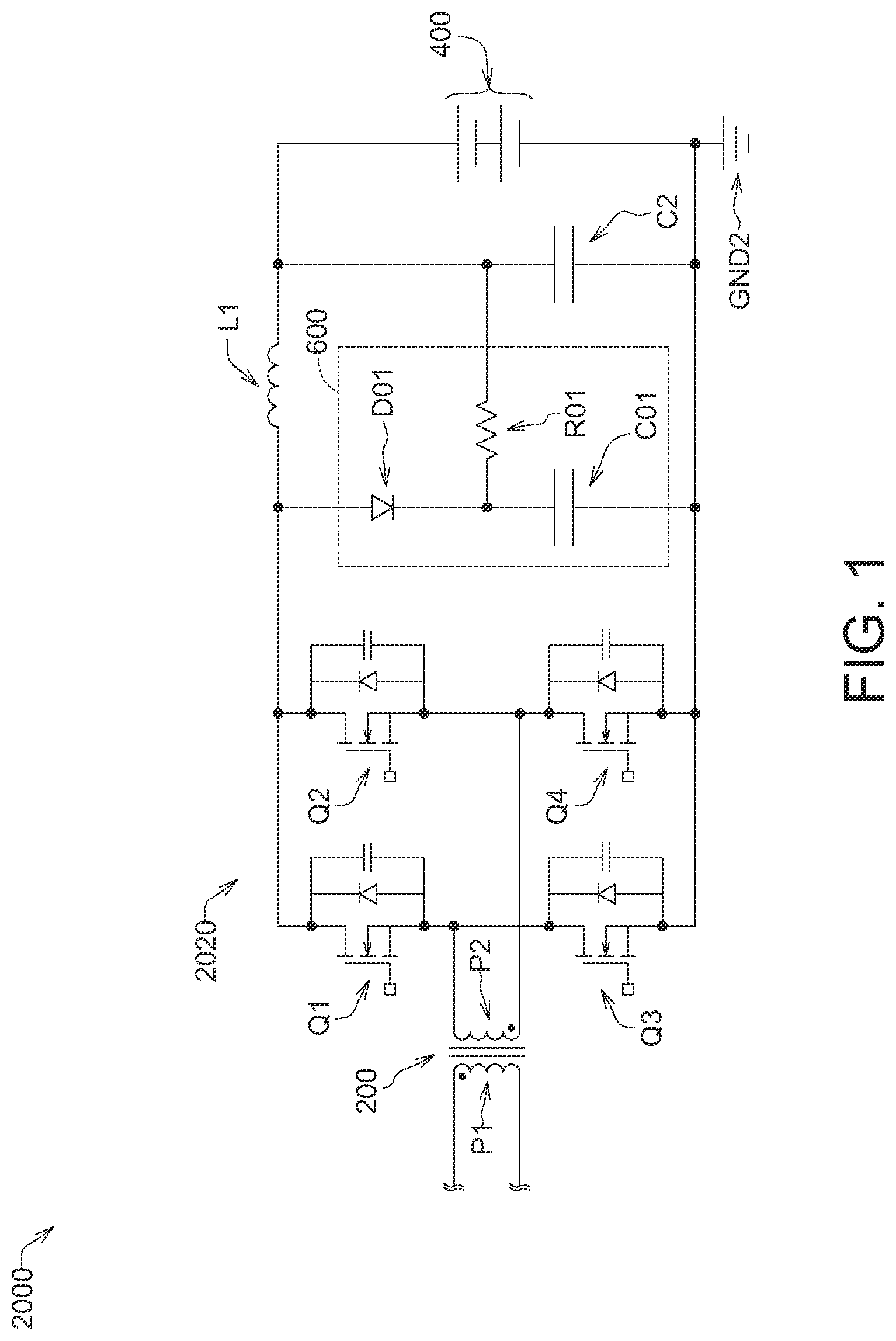
is a circuit diagram of a power conversion circuit 2000 in the prior art. only shows a secondary side circuit 2020 of the power conversion circuit 2000 . The transformer 200 has a primary side winding coil P 1 and a secondary side winding coil P 2 . The secondary side circuit 2020 is connected to the secondary side winding coil P 2 of the transformer 200 . The secondary side circuit 2020 comprises transistors Q 1 -Q 4 , a capacitor C 2 and a second power supply 400 . Transistors Q 1 -Q 4 serve as switching elements. When an abnormality occurs in the energy storage system, the transistors Q 1 -Q 4 are immediately disconnected, causing an instantaneous change in current, and the inductor L 1 will generate a huge surge voltage. A surge energy associated with the surge voltage may damage transistors Q 1 -Q 4 .
In order to reduce the surge energy associated with the surge voltage, the power conversion circuit 2000 in the prior art is further provided with a snubber circuit 600 to absorb the surge energy. The damping circuit 600 comprises a diode D 01 , a capacitor C 01 and a resistor R 01 . When the snubber circuit 600 is operating, the diode D 01 is turned on and absorbs the surge energy through the capacitor C 01 . However, since resistor R 01 consumes power during normal operation, losses will occur.
In response to the above-mentioned technical problems of the prior art, it is necessary to improve or replace the existing snubber circuit, so that the surge energy can be recovered and the loss can be reduced.
SUMMARY
According to one embodiment, the power conversion circuit includes the following elements. A first transformer, comprising a first winding coil and a second winding coil. A primary side circuit, connected to the first winding coil, the primary side circuit comprising a first power supply and a plurality of first switching units. A secondary side circuit, connected to the second winding coil, the secondary side circuit comprises a second power supply, a plurality of second switching units and a coupling circuit. When one of the first switching units and the second switching units generates a surge voltage, a surge energy associated with the surge voltage is guided to the second power supply through the coupling circuit.
BRIEF DESCRIPTION OF THE DRAWINGS
is a circuit diagram of a power conversion circuit 2000 in the prior art.
A is a circuit diagram of a power conversion circuit 1000 a according to an embodiment of the disclosure.
B is a detailed circuit diagram of the coupling circuit 300 a of A .
A is a circuit diagram of a power conversion circuit 1000 b according to another embodiment of the disclosure.
B is a detailed circuit diagram of the coupling circuit 300 b of A .
is a circuit diagram of a power conversion circuit 1000 c according to yet another embodiment of the disclosure.
In the following detailed description, for purposes of explanation, numerous specific details are set forth in order to provide a thorough understanding of the disclosed embodiments. It will be apparent, however, that one or more embodiments may be practiced without these specific details. In other instances, well-known structures and devices are schematically shown in order to simplify the drawing.
DETAILED DESCRIPTION
A is a circuit diagram of a power conversion circuit 1000 a according to an embodiment of the disclosure. As shown in A , the power conversion circuit 1000 a comprises a primary side circuit 1010 , a secondary side circuit 1020 and a transformer 200 . The primary side circuit 1010 is electrically isolated from the secondary side circuit 1020 through the transformer 200 . The transformer 200 comprises a winding coil P 1 and a winding coil P 2 . The winding coil P 1 is disposed on the primary side of the transformer 200 and the winding coil P 2 is disposed on the secondary side of the transformer 200 . The winding coil P 1 and the winding coil P 2 have a turns ratio TNP_R. The turns ratio TNP_R is: the number of turns TNP2 of the winding coil P 2 divided by the number of turns TNP1 of the winding coil P 1 . When the turns ratio TNP_R is greater than “1”, the primary side of the transformer 200 is a high voltage side and the secondary side is a low voltage side. When the turns ratio TNP_R is less than “1”, the primary side of the transformer 200 is the low voltage side and the secondary side is the high voltage side. According to different values of the turns ratio TNP_R, the primary side circuit 1010 is associated with the low voltage side or the high voltage side, and the secondary side circuit 1020 is associated with the high voltage side or the low voltage side.
The primary side circuit 1010 comprises a first power supply 100 , a capacitor C 1 and four transistors Q 5 -Q 8 . One end of the first power supply 100 is connected to the drain d 5 of the transistor Q 5 , and the other end of the first power supply 100 is connected to the source s 7 of the transistor Q 7 and the ground end GND1. The capacitor C 1 is connected to the first power supply 100 in parallel. One end of the capacitor C 1 is connected to the drain d 5 of the transistor Q 5 , and the other end of the capacitor C 1 is connected to the source s 7 of the transistor Q 7 and the ground end GND1.
Each of the transistors Q 5 -Q 8 can be used as a switching unit, which has the function of a switch. Each of the transistors Q 5 -Q 8 can be referred to as a “first switching unit”. In one example, the transistors Q 5 -Q 8 are connected to the primary side winding coil P 1 in a full-bridge configuration. The connection method of the full-bridge configuration of transistors Q 5 -Q 8 is as follows: the source s 5 of transistor Q 5 and the drain d 7 of transistor Q 7 are connected to the first end P 11 of the winding coil P 1 , and the source s 6 of transistor Q 6 and the drain d 8 of the transistor Q 8 is connected to the second end P 12 of the winding coil P 1 . The transistors Q 5 -Q 8 perform switching functions according to the full-bridge configuration, so to achieve the purpose of rectifying the power provided by the first power supply 100 .
On the other hand, the secondary side circuit 1020 comprises a second power supply 400 , a capacitor C 2 , four transistors Q 1 -Q 4 , and a coupling circuit 300 a . The first end 401 of the second power supply 400 serves as the output end of the second power supply 400 , and the first end 401 is connected to the drain d 2 of the transistor Q 2 through the coupling circuit 300 a . The second end 402 of the second power supply 400 is connected to the source s 4 of the transistor Q 4 and the ground end GND2. The capacitor C 2 is connected with the second power supply 400 in parallel. One end of the capacitor C 2 is connected to the drain d 2 of the transistor Q 2 through the coupling circuit 300 a , and the other end of the capacitor C 2 is connected to the source s 4 of the transistor Q 4 and the ground end GND2.
Similar to the transistors Q 5 -Q 8 of the primary side circuit 1010 , each of the transistors Q 1 -Q 4 of the secondary side circuit 1020 can be used as a switching unit, which has the function of switching. Each of the transistors Q 1 -Q 4 One can be referred to as the “second switching unit”. In one example, the transistors Q 1 -Q 4 are connected to the winding coil P 2 on the secondary side in a full-bridge configuration. The connection method of the full-bridge configuration of transistors Q 1 -Q 4 is as follows: the source s 1 of transistor Q 1 and the drain d 3 of transistor Q 3 are connected to the first end P 21 of the winding coil P 2 , and the source s 2 of transistor Q 2 and the drain d 4 of the transistor Q 4 is connected to the second end P 22 of the winding coil P 2 . The transistors Q 1 -Q 4 perform switching functions according to the full-bridge configuration, so as to rectify the power provided by the winding coil P 2 on the secondary side.
In the reverse boost mode of the power conversion circuit 1000 a , when an abnormality occurs in the system and the operation must be stopped immediately. The transistors Q 1 -Q 4 and transistors Q 5 -Q 8 , that function as switches, are changed from turned-on state to turned-off state in a very short time and cause a surge voltage in the cross voltage of the winding coil S 1 of the secondary circuit 1020 and a surge voltage in the cross voltage between the drain d 2 of the transistor Q 2 and the source d 4 of the transistor Q 4 . Surge energy associated with the surge voltage may cause damage to transistors Q 1 -Q 4 and transistors Q 5 -Q 8 . In order to reduce the negative impact of the surge voltage, the coupling circuit 300 a is used to guide the surge energy associated with the surge voltage, such that the surge energy is guided to the second power supply 400 and the second power supply 400 can recover the surge energy.
B is a detailed circuit diagram of the coupling circuit 300 a of A . Please refer to A and 2 B , the coupling circuit 300 a comprises a winding coil S 1 , a winding coil S 2 and a rectifying element. The rectifying element is, for example, a diode D 1 . The winding coil S 1 and the winding coil S 2 form a transformer 310 . The winding coil S 1 is disposed on the primary side of the transformer 310 , and the winding coil S 2 is disposed on the secondary side of the transformer 310 . The winding coil S 1 and the winding coil S 2 have a turns ratio TNS_R. The turns ratio TNS_R is: the number of turns TNS2 of the winding coil S 2 divided by the number of turns TNS1 of the winding coil S 1 . On the other hand, the diode D 1 serves as a rectifying element to control the direction of the output current of the secondary side winding coil S 2 .
The first end S 11 of the winding coil S 1 is connected to the drain d 2 of the transistor Q 2 , and the second end S 12 of the winding coil S 1 is connected to one end of the capacitor C 2 and the first end 401 of the second power supply 400 . On the other hand, the first end S 21 of the winding coil S 2 is connected to the ground end GND3, and the second end S 22 of the winding coil S 2 is connected to one end of the capacitor C 2 and the first end 401 of the second power supply 400 through the diode D 1 . The second end S 22 of the winding coil S 2 is connected to the anode D 11 of the diode D 1 , and the cathode D 12 of the diode D 1 is connected to one end of the capacitor C 2 and the first end 401 of the second power supply 400 .
The cross voltage between the first end 401 and the second end 402 of the second power supply 400 is the voltage difference Vo1, and the cross voltage between the first end S 11 and the second end S 12 of the winding coil S 1 is the voltage difference VLo. Furthermore, the cross voltage between the drain d 2 of the transistor Q 2 and the source d 4 of the transistor Q 4 is the voltage difference Vds_HL. The voltage difference Vds_HL is equal to the sum of the voltage difference Vo1 of the second power supply 400 and the voltage difference VLo of the winding coil S 1 . Furthermore, there is a forward bias voltage VD1 between the anode D 11 and the cathode D 12 of the diode D 1 .
In operation, when an abnormality occurs in the system and the transistors Q 1 -Q 4 and transistors Q 5 -Q 8 change to turned-off state in a very short time, it will cause the current to change instantaneously, resulting in a surge voltage in the cross voltage of the winding coil S 1 , and the surge voltage is reflected in the voltage difference VLo between the first end S 11 and the second end S 12 of the winding coil S 1 . It will cause a surge voltage in the cross voltage between the drain d 2 of the transistor Q 2 and the source d 4 of the transistor Q 4 , and this surge voltage is reflected in the voltage difference Vds_HL between drain d 2 and source d 4 .
Furthermore, the voltage difference VLo (having a surge voltage) of the winding coil S 1 is coupled to the winding coil S 2 on the secondary side, and a voltage difference VLo_cp is generated between the first end S 21 and the second end S 22 of the winding coil S 2 . The voltage difference VLo_cp of the winding coil S 2 is equal to a product of the voltage difference VLo of the winding coil S 1 and the turns ratio TNS_R. Since the first end S 21 of the winding coil S 2 is connected to the ground end GND3, a potential of the anode D 11 of the diode D 1 is equal to the voltage difference VLo_cp between the second end S 22 and the first end S 21 of the winding coil S 2 , as shown in Equation (1):
V D 11 = VLo_cp = V Lo × TNS_R ( 1 )
When the potential of the anode D 11 of the diode D 1 is greater than the sum of the forward bias voltage VD1 of the diode D 1 and the voltage difference Vo1 of the second power supply 400 , the diode D 1 is in a turned-on state, and the surge energy associated with the surge voltage can be guided to the second power supply 400 through the diode D 1 , so that the second power supply 400 can recover the surge energy. When a product of the voltage difference VLo of the winding coil S 1 and the turns ratio TNS_R meets the predefined condition, the potential VD11 of the anode D 11 of the diode D 1 reaches a sufficient potential so that the diode D 1 is turned on and can guide the surge energy. The predefined condition to turn on the diode D 1 is shown as Equation (2):
VLo_cp = V Lo × TNS_R = V D 11 > V D 1 + V o 1 ( 2 )
In order to turned on the diode D 1 to guide the surge energy, the turns ratio TNS_R of the winding coil S 1 and the winding coil S 2 is set according to Equation (3):
TNS_R > V D 1 + V o 1 V Lo ( 3 )
A first value can be defined in Equation (3), where the first value is equal to the sum of the forward bias voltage VD1 of the diode D 1 and the voltage difference Vo1 of the second power supply 400 divided by the voltage difference VLo of the third winding coil S 1 . The first value is smaller than the turns ratio TNS_R of the winding coil S 1 and the winding coil S 2 .
A is a circuit diagram of a power conversion circuit 1000 b according to another embodiment of the disclosure. The power conversion circuit 1000 b of A is similar to the power conversion circuit 1000 a of A , and the difference lies in that, the coupling circuit 300 b of the power conversion circuit 1000 b of A comprises a different form of rectifying element. The rectifying element of coupling circuit 300 b is replaced by transistor Q 9 . The transistor Q 9 can be used as a switching unit having a function of switching. The transistor Q 9 can be referred to as “the third switching unit”. The transistor Q 9 serves as a rectifier element to control the current output of the winding coil S 2 on the secondary side of the transformer 310 .
B is a detailed circuit diagram of the coupling circuit 300 b of A . Please refer to A and 3 B , the coupling circuit 300 a comprises a winding coil S 1 , a winding coil S 2 and a transistor Q 9 . The second end S 22 of the winding coil S 2 is connected to one end of the capacitor C 2 and the first end 401 of the second power supply 400 through the transistor Q 9 . The second end S 22 of the winding coil S 2 is connected to the source s 9 of the transistor Q 9 , and the drain d 9 of the transistor Q 9 is connected to one end of the capacitor C 2 and the first end 401 of the second power supply 400 .
The potential Vs9 of the source s 9 of the transistor Q 9 is equal to the voltage difference VLo_cp of the winding coil S 2 , and is equal to the product of the voltage difference VLo of the winding coil S 1 and the turns ratio TNS_R, as shown in Equation (4):
V d 9 = VLo_cp = V Lo × TNS_R ( 4 )
When the turns ratio TNS_R of the winding coil S 1 and the winding coil S 2 is set as an appropriate value, and the product of the voltage difference VLo of the winding coil S 1 and the turns ratio TNS_R meets the predefined condition, thereby making the potential Vd9 of the drain d 9 of the transistor Q 9 meets a condition for turning on the transistor Q 9 , transistor Q 9 can be turned on to guide surge energy. The surge energy is guided to the second power supply 400 through the transistor Q 9 to recover the surge energy.
In other embodiments, the coupling circuit of the power conversion circuit may use other forms of rectifying elements than the diode D 1 in B and the transistor Q 9 in B , such as other forms of switching elements.
In the embodiments of A, 2 B, 3 A, and 3 B , the coupling circuits 300 a and 300 b are disposed in the secondary side circuit 1020 and are associated with the secondary side of the transformer 200 . The secondary side can be the high voltage side or the low voltage side. When the turns ratio TNP_R of the winding coil P 1 and the winding coil P 2 is greater than “1”, the secondary side is the low voltage side. When the turns ratio TNP_R is less than “1”, the secondary side is the high voltage side. In other embodiments (not shown in the figures), the coupling circuits 300 a and 300 b may be disposed in the primary side circuit 1010 , which is associated with the primary side of the transformer 200 . Moreover, in other embodiments (not shown in the figures), the transistors Q 1 to Q 4 and the transistors Q 5 to Q 8 providing switching functions may be other forms of switching elements. In addition, the power conversion circuits 1000 a and 1000 b can operate actively in duplex directions, and have current-feeding capabilities.
is a circuit diagram of a power conversion circuit 1000 c according to yet another embodiment of the disclosure. The power conversion circuit 1000 c in is similar to the power conversion circuit 1000 a in A , with the difference lies in that, the coupling circuit 300 c of the power conversion circuit 1000 c in has a different connection method.
As shown in , the second end S 22 of the winding coil S 2 of the coupling circuit 300 c is connected to the first end 101 of the first power supply 100 through the diode D 1 (the first end 101 is the positive end). The second end S 22 of the winding coil S 2 is connected to the anode of the diode D 1 , and the cathode of the diode D 1 is connected to the first end 101 of the first power supply 100 . The first power supply 100 is a voltage source. Therefore, in this embodiment, “clamping limitation” can be performed by the first power supply 100 .
Through the above embodiments, the power conversion circuits 1000 a and 1000 b of the present disclosure can guide the surge energy associated with the surge voltage to the second power supply 400 through the coupling circuits 300 a and 300 b , so as to recover the surge energy. Compared with the energy loss that occurs when the snubber circuit 600 of the prior art handles surge energy, the coupling circuits 300 a and 300 b of the present disclosure can recycle the surge energy to the second power supply 400 , hence the energy loss can be to significantly reduced. Moreover, through the connection between the coupling circuit 300 c and the first power supply 100 , the power conversion circuit 1000 c of the present disclosure achieves an effect of “clamping limitation”.
It will be apparent to those skilled in the art that various modifications and variations can be made to the disclosed embodiments. It is intended that the specification and examples be considered as exemplars only, with a true scope of the disclosure being indicated by the following claims and their equivalents.
Figures (6)
Citations
This patent cites (6)
- US5615094
- US9584028
- US9923474
- US2008/0285311
- US2022/0294345
- US115085554