Dual Power Supply Transfer Switch Based on Solid-state Switch
Abstract
A dual power supply transfer switch (SSATS) for switching between a first power supply (S 1 ) and a second power supply (S 2 ) to supply power to a load is provided, includes: a solid-state switch (SS); a mechanical switch (CTR); and a compensation power module (AUX). In the case that the S 1 fails in supplying power to the load, the AUX uses the S 2 to supply power to the load, and the output current of the S 1 is reduced. After satisfying the turn off condition for the SS, the SS turns off the S 1 , the CTR turns off the S 1 and turns on the S 2 . After the S 2 is adjusted to synchronize with the phase of the output current of the S 1 , the SS turns on the S 2 and the AUX stops outputting current. The SSATS provides advantages such as fast transfer, zero interruption, and short voltage sag time.
Claims (18)
1 . A dual power transfer switch for supplying uninterrupted power to a load, comprising: a first solid-state switch configured to selectively connect the load to a first AC power supply providing AC electrical power of a first phase; a second solid-state switch configured to selectively connect the load to a second AC power supply providing AC electrical power of a second phase; a first mechanical switch in series with the first solid-state switch; a second mechanical switch in series with the second solid-state switch; and a power supply unit configured to selectively receive AC electrical power from a selected one of the first and second power supplies, and to provide AC electrical power of a controlled phase to the load, wherein, during normal operation, the second solid-state switch is open and the first solid-state switch is closed, thereby connecting the load to the first power supply; a controller configured to: cause the power supply unit to receive AC electrical power of the second phase from the second power supply and to convert the AC electrical power of the second phase received therefrom to AC electrical power of the first phase; monitor the first power supply to detect a failure of the first power supply; and in response to detecting the failure of the first power supply: cause the first solid-state switch to open, thereby isolating the load from the first power supply; cause the power supply unit to provide the AC electrical power of the first phase to the load; cause the first mechanical switch to open and the second mechanical switch to close after causing the first solid-state switch to open; cause the power supply unit to transition the controlled phase of the AC electrical power provided to the load from the first phase to the second phase; and cause the second solid-state switch to close in response to the controlled phase of the AC electrical power provided by the power supply unit being synchronized with the second phase of the AC electrical power received from the second power supply, thereby connecting the load to the second power supply.
Show 17 dependent claims
2 . The dual power transfer switch of claim 1 , wherein the controller causes the first solid-state switch to open in response to AC electrical current provided by the first power supply falling below a first current threshold.
3 . The dual power transfer switch of claim 1 , wherein the controller causes the first solid-state switch to open in response to AC electrical voltage provided by the power supply unit exceeding a predetermined voltage threshold.
4 . The dual power transfer switch of claim 1 , wherein the controller causes the first solid-state switch to open in response to AC electrical current provided by the power supply unit exceeding a predetermined current threshold.
5 . The dual power transfer switch of claim 1 , wherein the controller is further configured, in response to detecting the failure of the first power supply, to: cause the power supply unit to receive AC electrical power of the first phase from the first power supply and to convert the AC electrical power of the first phase received therefrom to AC electrical power of the second phase.
6 . The dual power transfer switch of claim 1 , wherein the controller is further configured to cause the second mechanical switch to close before causing the second solid-state switch to close.
7 . The dual power transfer switch of claim 1 , wherein the first and second mechanical switches are configured as a single-pole double-throw switch.
8 . The dual power transfer switch of claim 7 , wherein the second solid-state switch is closed after the first solid-state switch is opened.
9 . The dual power transfer switch of claim 1 , further comprising: a third mechanical switch configured to selectively connect the first power supply to an input of the power supply unit; and a fourth mechanical switch configured to selectively connect the second power supply to the input of the power supply unit.
10 . The dual power transfer switch of claim 9 , wherein the third and fourth mechanical switches are configured as a single-pole double-throw switch.
11 . The dual power transfer switch of claim 1 , wherein the power supply unit comprises: a first AC to DC converter configured to convert the AC electrical power selectively received from the first power supply to DC electrical power; a second AC to DC converter configured to convert the AC electrical power selectively received from the second power supply to DC electrical power; and a three-phase inverter unit configured to receive the DC electrical power from the first and second AC to DC converters and to generate therefrom the AC electrical power of the controlled phase.
12 . The dual power transfer switch of claim 1 , wherein the first solid-state switch has three bridge arms, each configured to receive a corresponding phase of three-phase AC electrical power of the first phase provided by the first power supply, the second solid-state switch has three bridge arms, each configured to receive a corresponding phase of three-phase AC electrical power of the second phase provided by the second power supply, and the power supply unit is a three-phase power supply unit configured to generate three-phase AC electrical power of the controlled phase.
13 . The dual power transfer switch of claim 12 , wherein the power supply unit comprises: an AC to DC converter configured to convert the AC electrical power selectively received from the first or second power supplies to DC electrical power; and a three-phase inverter unit configured to receive the DC electrical power from the AC to DC converter and to generate therefrom the AC electrical power of the controlled phase.
14 . The dual power transfer switch of claim 13 , wherein the AC to DC converter comprises a high-frequency transformer.
15 . The dual power transfer switch of claim 13 , wherein the AC to DC converter comprises a power frequency transformer.
16 . The dual power transfer switch of claim 1 , wherein each of the first and second solid-state switches comprises a bidirectional switch array, wherein the bidirectional switch array is formed through a thyristor, a metal oxide semiconductor field effect transistor (MOSFET), or an insulated gate bipolar transistor (IGBT).
17 . The dual power transfer switch of claim 16 , wherein the bidirectional switch array comprises a reverse parallel pair of thyristors, or MOSFETs, or IGBT transistors.
18 . The dual power transfer switch of claim 1 , wherein the controller is further configured, in response to detecting the failure of the first power supply, to: cause the power supply unit to provide the AC electrical power of the first phase to the load before causing the first solid-state switch to open, thereby temporarily providing the AC electrical power of the first phase to the load from both the first power supply and the power supply unit.
Full Description
Show full text →
CROSS REFERENCE TO RELATED APPLICATIONS
The present application is a 35 U.S.C. § 371 National Phase Application of International PCT Patent Application No. PCT/CN2023/105027, filed Jun. 30, 2023, which claims the benefit of priority of Chinese Patent Application No. CN 202210770934.8, filed on Jun. 30, 2022. The entire contents of these applications are incorporated herein by reference in their entirety.
TECHNICAL FIELD
The present disclosure relates to a dual power supply transfer, and more specifically, to a dual power supply transfer switch based on a solid-state switch.
BACKGROUND
At present, the dual power supply transfer scheme with uninterrupted load is an automatic transfer switch (ATS) and uninterruptible power supply (UPS) architecture. The ATS is a simple mechanical structure, subject to inherent drawbacks of the mechanical structure. And the traditional ATS switching time is often greater than 100 ms, which is often unacceptable for some devices sensitive to power-down time. Therefore, for such loads, (The) ATS cannot independently complete power supply switching and often needs to cooperate with the UPS to meet the demand for supplying power to the load uninterruptedly. Specifically, the ATS is connected to two power supplies to switch between them, and when it is switching, supplying power to the load during the short-time switching power-down process is maintained by cooperating with the UPS.
SUMMARY
Technical Problem
Based on the ATS and UPS architecture, continuous supplying power to the load side can be implemented, but there are the following drawbacks. Since the ATS switching process results in a power-down on the UPS input side, and the power-down duration may be up to 500 ms. In addition, the ATS uses mechanical switch (CTR) to switch power supply output, so when the power supply is switching, the CTR may experience arcing phenomenon. In addition, the ATS and UPS architectures cannot track a phase difference between the two power supplies.
On the other hand, maintaining supplying power to the load side requires an internal battery pack of the UPS. For loads above 100 A, a larger battery pack is required. At the same time, in order to maintain the continuity of supplying power to the load, the modules of the UPS must be online for a long period of time, which results in a relatively low power transfer efficiency.
Solution to Problem
According to one aspect of the present disclosure, a dual power supply transfer switch (SSATS) for switching between a first power supply (S 1 ) and a second power supply (S 2 ) to supply power to a load is provided, including: a solid-state switch (SS), through which the S 1 or the S 2 is connected to the load; and a compensation power supply module (AUX), through which the S 1 or the S 2 is connected to the load. The S 2 is used to supply power to the load through the compensation power supply module in the case that the S 1 fails in supplying power to the load. The S 1 is turned off from the power supply side through the SS in a case where an output current or output voltage of the AUX satisfies a first condition, and in a case where a phase of the AUX satisfies the second condition, the S 2 is used to supply power to the load through the SS, and the AUX stops supplying power to the load.
In some embodiments, the SS includes: a first SS, which is connected to the S 1 for connecting the S 1 switch to the load; and a second SS, which is connected to the S 2 for connecting the S 2 switch to the load.
In some embodiments, the SS is a single SS.
In some embodiments, the SSATS includes: a first mechanical switch (CTR 1 ), wherein the S 1 is connected to the load through the CTR 1 and the first SS; a second mechanical switch (CTR 2 ), wherein the S 2 is connected to the load through the CTR 2 and the second SS. The CTR 1 is turned off and the CTR 2 is turned on, after the S 1 is turned off from the power supply side through the SS.
In some embodiments, the SSATS includes a fifth mechanical switch (CTR 1 / 2 ), configured as a single-pole, double-throw switch and through which the S 1 or the S 2 is connected to a load. The S 2 is connected to the load through the CTR 1 / 2 , after the S 1 is turned off from the power supply side through the SS.
In some embodiments, the SS includes a bidirectional switch array, wherein the bidirectional switch array is formed through a thyristor, an insulated gate bipolar transistor (IGBT) or a metal oxide semiconductor field effect transistor (MOSFET).
In some embodiments, the bidirectional switch array includes a thyristor in reverse parallel, or a MOSFET or IGBT transistor in reverse series.
In some embodiments, the AUX includes an AC-DC converter (AC/DC) and a three-phase inverter unit (VSI) in series.
In some embodiments, the AC/DC includes: a first AC/DC connected between the S 1 and the VSI; and a second AC/DC connected between the S 2 and the VSI, wherein, the first AC/DC and the second AC/DC are connected in parallel to the VSI.
In some embodiments, the AUX includes: a third mechanical switch (CTR 3 ) connected between the S 1 and the AC/DC; and a fourth mechanical switch (CTR 4 ) connected between the S 2 and the AC/DC, wherein, upon the S 1 supplying power to the load, the CTR 3 is turned off and the CTR 4 is turned on, and upon the S 2 supplying power to the load, the CTR 3 is turned on, and the CTR 4 is turned off.
In some embodiments, the AUX includes a sixth mechanical switch (CTR 3 / 4 ) configured as a single-pole double-throw switch connected to the S 1 and the S 2 , wherein, upon the S 1 supplying power to the load, the S 2 is connected to the AC/DC through the CTR 3 / 4 , and upon the S 2 supplying power to the load, the S 1 is connected to the AC/DC through the CTR 3 / 4 .
In some embodiments, the AC/DC includes a high-frequency transformer.
In some embodiments, the AC/DC includes a power frequency transformer.
In some embodiments, the first condition is that the output current of the AUX reaches a first threshold.
In some embodiments, the first condition is that the output voltage of the AUX reaches a second threshold.
In some embodiments, the second condition is that the phase of the AUX is synchronized with the phase of the S 2 .
Advantageous Effects of Invention
Compared to the existing ATS and UPS architectures, the SSATS of the present disclosure may provide advantages such as fast transfer, zero interruption, and short voltage sag time, etc. through the use of SS and AUX, and is not subject to the effects of an ATS arcing, and may also track the phase of the failure power supply during the transfer process. In addition, compared to the UPS, the SS has lower losses, eliminates the need for periodic battery replacement, and the configuration of the SS and power supply unit (PSU) may avoid the effect of switch arcing.
BRIEF DESCRIPTION OF DRAWINGS
The above and other aspects, features, and advantages of the specific embodiments disclosed herein will become more apparent from the following description combined with the accompanying drawings, and in which:
is a schematic diagram of a SSATS according to embodiments of the present disclosure;
is a schematic diagram of a detailed structure of a SSATS according to embodiments of the present disclosure;
to 6 are schematic diagrams of detailed structures of other SSATSes according to embodiments of the present disclosure;
is a schematic diagram of a detailed structure of a thyristor/Silicon Controlled Rectifier (SCR) according to embodiments of the present disclosure;
are schematic diagrams of detailed structures of other SCRs according to embodiments of the present disclosure;
is a schematic diagram of a detailed structure of a PSU according to embodiments of the present disclosure;
are schematic diagrams of detailed structures of other PSUs according to embodiments of the present disclosure;
is a schematic diagram of timing of the simulation of a SSATS according to embodiments of the present disclosure; and
is a graph of simulation results of a SSATS according to embodiments of the present disclosure.
DETAILED DESCRIPTION
Before undertaking the detailed description below, it may be advantageous to set forth definitions of certain words and phrases used throughout this application document. The terms “include” and “comprise,” as well as derivatives thereof, mean inclusion without limitation. The term “or” is inclusive, meaning and/or. The phrase “associated with,” as well as derivatives thereof, means include, be included within, interconnect with, comprise, be comprised within, connect to or with, couple to or with, communicate with, cooperate with, interleave, juxtapose, be proximate to, be bound to or with, have, have a property of, have a relationship to or with, or the like. The term “controller” means any device, system, or part thereof that controls at least one operation. Such a controller may be implemented in hardware or a combination of hardware and software and/or firmware. The functionality associated with any particular controller may be centralized or distributed, whether locally or remotely. The phrase “at least one of,” when used with a list of items, means that different combinations of one or more of the listed items may be used, and only one item in the list may be needed. For example, “at least one of: A, B, and C” includes any one of the following combinations: A, B, C, A and B, A and C, B and C, and A and B and C.
Definitions for other specific words and phrases are provided throughout this application document. Those of ordinary skill in the art should understand that in many if not most cases, such definitions apply to prior as well as future uses of such defined words and phrases.
In this application document, the application combinations of transform blocks and the hierarchy division of sub-transform blocks are used for illustrative purposes only, and the combinations of applications of transform blocks and the hierarchy of divisions of sub-transform blocks may be characterized in different ways without departing from the scope of the present disclosure.
through , discussed below, and the various embodiments used to describe the principles of the present disclosure in this application document are for illustration purposes only and should not be construed in any way to limit the scope of the present disclosure. Those skilled in the art will appreciate that the principles of the present disclosure may be implemented in any suitably arranged system or device.
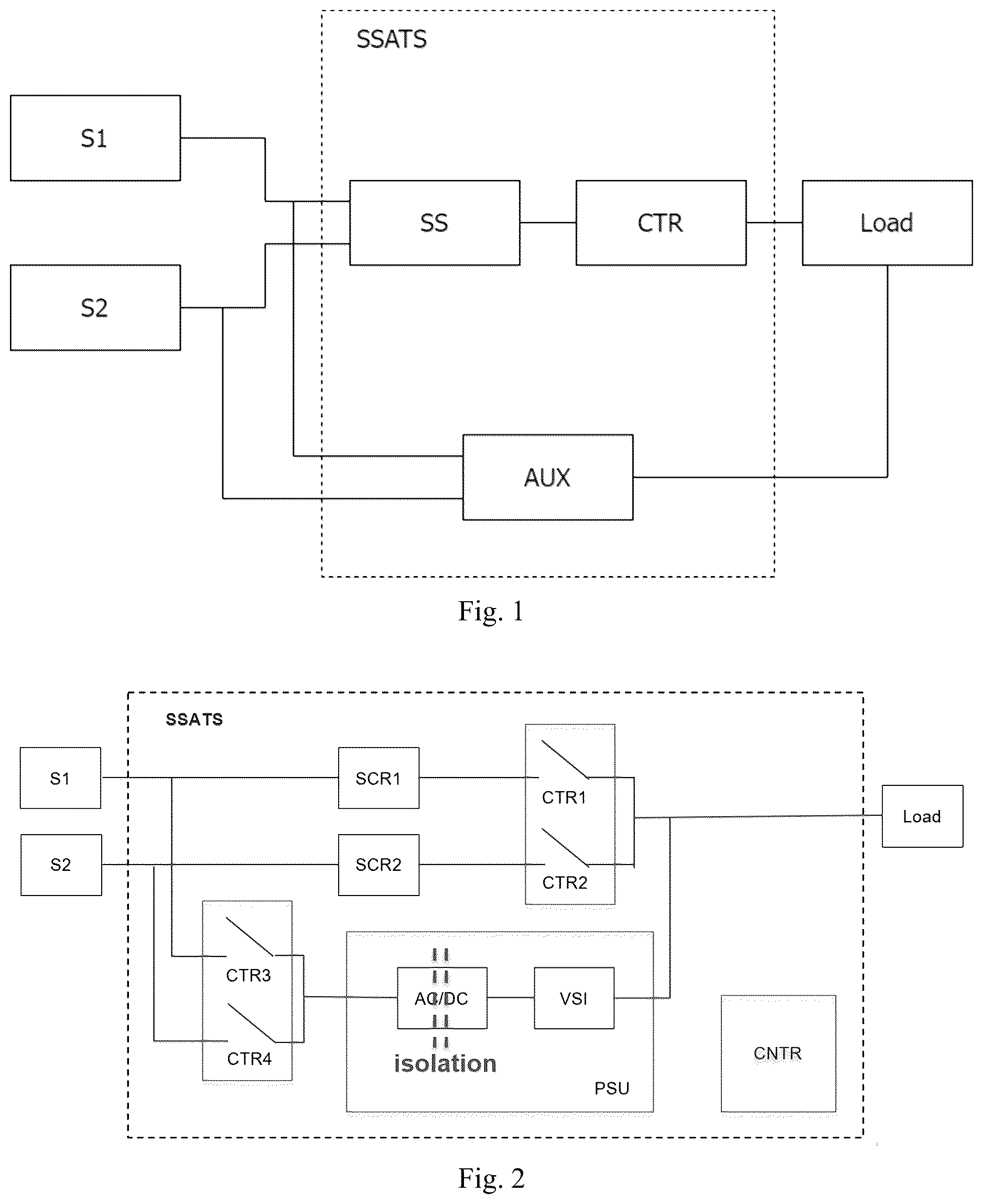
is a schematic diagram of a SSATS according to embodiments of the present disclosure.
As shown in , the SSATS includes a SS, a CTR, and a AUX. The SS is used to switch the S 1 and the S 2 to supply power to the load, and may include one or more SSes composed of semiconductor switches, such as SCR. The CTR physically isolates the S 1 and the S 2 , and may be one or more CTRs that are separate or integral, independently controlled or interlocked. In addition, the positions of the SS and the CTR may be changed, and the same effect may be achieved by performing the same operating steps. The compensation power supply module includes an AC/DC and an inverter, where the AC/DC converts the three-phase current and voltage of the S 1 or the S 2 into DC current and voltage, and the inverter converts DC current and voltage into a three-phase current and voltage that have been phase adjusted.
The S 1 and the S 2 are connected to the load through the SS and the CTR, respectively. In addition, the S 1 and the S 2 are also connected to the load through the AUX, respectively. In the normal operating state of the S 1 supplying power to the load, the SS and the CTR turn on the S 1 and the load, and turn off the S 2 and the load. The AUX turns on the S 2 and turns off S 1 . In this situation, the S 1 supplies power to the load as the main power supply, and the S 2 serves as the backup power supply.
When the S 1 fails (such as overvoltage, undervoltage, power-down, frequency overrun, overload, etc.), the AUX uses the S 2 to supply power to the load, and the output current of the AUX is adjusted until the first condition is satisfied. The phase of the AUX is controlled to be synchronized with the phase of the S 1 . The first condition may be that the output current of the AUX reaches the first threshold, or the output voltage of the AUX reaches the second threshold. In this situation, the SS turns off the S 1 . Because the SS is a contactless switch, there is no arcing phenomenon caused by the voltage between the contacts breaking through the air layer during turning on and turning off.
Then, the CTR turns off the S 1 , and subsequently, if the phase of the S 1 (i.e., the current phase of the AUX) and the phase of the S 2 are not synchronized, the phase of the AUX is adjusted to be synchronized with the phase of the S 2 . When the phase of the AUX satisfies the second condition, the CTR and the SS turn on the S 2 , so that the S 2 directly supplies power to the load through the SS and the CTR, and the AUX stops using the S 2 to supply power to the load. The second condition may be that the phase of the AUX is synchronized with the phase of the S 2 . In addition, the AUX turns on the S 1 and turns off the S 2 . In this situation, the S 2 continues to supply power to the load as the main power supply, and the S 1 serves as the backup power supply.
In other embodiments, the CTR and its operation may be omitted, and only the S 1 and the S 2 are switched by the SS without physically isolating the S 1 and the S 2 .
is a schematic diagram of a detailed structure of a SSATS according to embodiments of the present disclosure. The SSATS in corresponds to the SSATS in .
As shown in , the SSATS includes a first SCR (SCR 1 ) and a second SCR (SCR 2 ), a CTR 1 to a CTR 4 , a PSU, and a control unit (CNTR). The PSU includes an AC/DC and a VSI. The SCR 1 and the SCR 2 correspond to the SS in , the CTR 1 and the CTR 2 correspond to the CTR in , the CTR 3 , the CTR 4 , and the PSU correspond to the AUX in . The CTR 1 and the CTR 2 provide isolation between the S 1 and the S 2 , and the CTR 3 and the CTR 4 also provide isolation between the S 1 and the S 2 . The CNTR may be any component that performs the functions described below, such as a circuit, processor, etc.
The S 1 is connected to the load through the SCR 1 and the CTR 1 , and the S 2 is connected to the load through the SCR 2 and the CTR 2 . In addition, the S 1 is also connected to the load through the CTR 3 and the PSU, and the S 2 is also connected to the load through the CTR 4 and the PSU. In the normal operating state in which the S 1 supplies power to the load, the SCR 1 , the CTR 1 , and the CTR 4 are in a turning on state, the SCR 2 , the CTR 2 , and the CTR 3 are in a turning off state, and the CNTR continuously detects the state of the S 1 . In this situation, the S 1 supplies power to the load as the main power supply, and the S 2 serves as the backup power supply.
When the CNTR detects a failure of the S 1 , the drive of the bridge arm of the SCR 1 is turned off, and the CNTR tracks the phase of the S 1 , so as to control the PSU to use the S 2 to output the three-phase current and voltage required for load. The AC/DC converts the three-phase current and voltage of the S 2 into DC current and voltage, and the VSI converts DC current and voltage into a three-phase current and voltage synchronized with the phase of the S 1 . In this situation, the S 1 and the PSU using the S 2 simultaneously supply power to the load.
The CNTR controls the PSU to gradually increase the three-phase current and voltage, while the current passing through the SCR 1 decreases until the output current of the PSU reaches the first threshold or the output voltage of the PSU reaches the second threshold. The first threshold may be the current required for the load (i.e., the current output by the S 1 before the failure), such that the SCR 1 turns off at zero-crossing due to the current dropping to zero. Those skilled in the art will appreciate that the first threshold may be other value that is set to be greater or less than the current required for the load as desired, and the first threshold may be used as a triggering condition to turn off the SCR 1 in other ways. Similarly, the second threshold may be the voltage required for the load, or other value that is set to be greater or less than the voltage required for the load as desired, and the second threshold may be used as a triggering condition to turn off the SCR 1 in other ways.
When the SCR 1 is turned off, the CNTR may control the CTR 1 to turn off and the CTR 2 to turn on. Moreover, since the SCR 1 is turned off, the possible arcing phenomenon generated by the CTR 1 does not affect the load. In addition, the CNTR detects whether the phase of the S 1 (i.e. the current phase of the PSU) is synchronized with the phase of the S 2 . If it is not synchronized, the CNTR controls the PSU to adjust the phase until the phase of the PSU is synchronized with the phase of the S 2 .
When the phase of the PSU is synchronized with the phase of the S 2 , the CNTR controls the SCR 2 to turn on and the PSU to stop outputting, so that the S 2 directly supplies power to the load through the SS and the CTR. In addition, the CNTR controls the CTR 4 to turn off and the CTR 3 to turn on, so as to turn on the S 1 and turn off the S 2 . In this way, the S 2 continues to supply power to the load as the main power supply, and the S 1 is served as the backup power supply.
is a schematic diagram of a detailed structure of other SSATSes according to embodiments of the present disclosure. The SSATS in corresponds to the SSATS in .
In the SSATS shown in , the CTR 1 and the CTR 2 are replaced with a CTR 1 / 2 , and the CTR 1 / 2 is a single-pole, double-throw switch. That is, for the CTR 1 / 2 , turning on the S 1 is equivalent to turning off the S 2 , and turning off the S 1 is equivalent to turning on the S 2 . Similarly, the CTR 3 and the CTR 4 are replaced with the CTR 3 / 4 , and the CTR 3 / 4 is a single-pole double-throw switch. That is to say, for the CTR 3 / 4 , turning on the S 1 is equivalent to turning off the S 2 , and turning off the S 1 is equivalent to turning on the S 2 .
is a schematic diagram of a detailed structure of other SSATSes according to embodiments of the present disclosure. The SSATS in corresponds to the SSATS in .
In the SSATS shown in , compared to the SSATS in , the positions of the CTR 1 and the CTR 2 are switched with the positions of the SCR 1 and the SCR 2 , and the same function can still be realized.
is a schematic diagram of a detailed structure of other SSATSes according to embodiments of the present disclosure. The SSATS in corresponds to the SSATS in .
In the SSATS shown in , the SCR 1 and SCR 2 are replaced with a single SCR SCR 1 / 2 . Compared to the implementation shown in , turning off the single SCR SCR 1 / 2 is equivalent to turning off the SCR 1 , and turning on the single SCR SCR 1 / 2 is equivalent to turning on the SCR 2 .
is a schematic diagram of a detailed structure of other SSATSes according to embodiments of the present disclosure. The SSATS in corresponds to the SSATS in .
In the SSATS shown in , the CTR 3 , the CTR 4 , and the AC/DC are replaced with the first AC/DC connected to the S 1 and the second AC/DC connected to the S 2 , and the first AC/DC and the second AC/DC are also connected in parallel to the VSI. Therefore, the operations of the CTR 3 and the CTR 4 may be omitted, while maintaining isolation between the S 1 and the S 2 .
is a schematic diagram of a detailed structure of a thyristor/Silicon Controlled Rectifier (SCR) according to embodiments of the present disclosure. The SCR in corresponds to the SCR 1 and SCR 2 in .
In the SCR shown in , the SCR includes a bidirectional switch array corresponding to a three-phase power supply without neutral line, however, the present disclosure is not limited to thereto, and the SCR may correspond to other types of power supplies and employ a structure for other types of power supplies, in order to achieve a function similar to that of the SCR shown in . The bidirectional switch array has three bridge arms, each with two unidirectional SCRs in reverse parallel. With this configuration, positive or negative current can activate the gate of either of the two unidirectional SCRs, allowing AC current to pass through. When the current passing through either of the unidirectional SCRs falls below a threshold, the unidirectional SCRs cause the entire SCR to turn off, so as to enable bidirectional switch control. External circuits or components (such as the CNTR) may transmit control signals to the unidirectional SCRs to turn on the unidirectional SCRs. Those skilled in the art will understand the specific structure and related details of the unidirectional SCRs, therefore the description will be omitted in the present disclosure.
are schematic diagrams of detailed structures of other SCRs according to embodiments of the present disclosure. The SCR in corresponds to the SCR 1 and SCR 2 in , respectively.
In the SCRs shown in , the SCRs include a bidirectional switch array corresponding to the three-phase power supply without neutral line, however, the present disclosure is not limited thereto, and the SCRs may correspond to other types of power supplies and employ a structure for other types of power supplies in order to achieve similar functions as the SCRs shown in . The bidirectional switch array has three bridge arms, each with two positive channel metal oxide semiconductor (PMOS) transistors in reverse series, such as IGBT or MOSFET. illustrate two specific implementations of reverse series, respectively. With this configuration, the voltage drop of the diode may be avoided and reverse polarity protection may be provided. External circuits or components (such as the CNTR) may transmit control signals to the PMOS transistors to turn on the PMOS transistors. Those skilled in the art will understand the specific structure and related details of the PMOS transistors (such as IGBT or MOSFET), therefore the description will be omitted in the present disclosure.
is a schematic diagram of a detailed structure of a PSU according to embodiments of the present disclosure. The PSU in corresponds to the PSU in .
In the detailed structure of the PSU shown in , the first AC/DC and the second AC/DC are replaced with high-frequency transformers so as to directly provide isolation between the S 1 and the S 2 , and also convert the three-phase current and voltage into DC current and voltage to output to the VSI.
are schematic diagrams of detailed structures of other PSUs according to embodiments of the present disclosure. The PSUs in correspond to the PSU in .
In the detailed structure of the other PSU shown in , the first AC/DC and the second AC/DC are replaced with a power frequency transformer and an AC/DC, and the power frequency transformer, the AC/DC, and the VSI are connected in series. The power frequency transformer first receives uninsulated three-phase voltage and current output from the S 1 or the S 2 , and performs adjustments (for example, when there is a voltage fluctuation in the S 1 due to a failure, the power frequency transformer adjusts the uninsulated three-phase voltage to a stable level three-phase voltage), and then outputs the adjusted three-phase voltage and current to the AC/DC. The AC/DC converts three-phase voltage and current into DC current and voltage, and the VSI converts DC current and voltage into a three-phase voltage and three-phase current required by the load to provide it to the load.
In the detailed structure of the other PSU shown in , the first AC/DC and the second AC/DC are replaced with an AC/DC, and a power frequency transformer provided between the VSI and the load, and the AC/DC, the VSI, and the power frequency transformer are connected in series. The AC/DC converts the uninsulated three-phase current and voltage output by the S 1 or the S 2 into DC current and voltage, and the VSI converts DC current and voltage into a three-phase current and an unexpected three-phase voltage required by the load. Then, the power frequency transformer adjusts the unexpected three-phase voltage to provide the three-phase current and voltage required by the load to the load.
is a schematic diagram of timing of simulation of a SSATS according to embodiments of the present disclosure, and is a graph of results of the simulation of a SSATS according to embodiments of the present disclosure. The SSATSes in may correspond to the SSATS in .
As shown in , t 0 indicates a time point when the S 1 fails (such as voltage sag), t 1 indicates a time point when the S 1 fails, the drive of the bridge arm of the SCR 1 is turned off, and the PSU supplies power to the load. t 2 indicates the time point when the CTR 1 is turned off, and t 3 indicates the time point when the CTR 2 is turned on, and t 4 indicates the time point when the phase synchronization between the PSU and the S 2 is completed. The period from t 0 to t 1 is less than 1 ms, the period from t 1 to t 2 is less than 1 ms, the period from t 2 to t 3 is in the range of 50 ms to 200 ms, and the period from t 1 to t 4 (i.e. the entire period from detecting the S 1 fails to directly supplying power to the load by the S 2 ) may be less than 1 s.
As shown in , the left half of shows the changes in voltage and current of the S 1 over time, the right half of shows the changes in voltage and current of the S 2 over time, and in the dashed box of , it shows the changes in voltage and current of the load over time. In the first and second graphs from top to bottom in the left half of , there is an abnormal fluctuation in the current of the S 1 at the beginning. At about 20 ms (0.02), the failure of the S 1 is detected, and the PSU is changed to supply power to the load, so that the output current of the S 1 is zero, and the S 1 could be turned off. In the first graph from top to bottom in the right half of , at about 50 ms (0.05), the S 2 directly supplies power to the load.
Referring to the graph in the dashed line section, the load is only affected by voltage sag within about 3 ms after 20 ms, and the power supply to the load is not interrupted throughout the entire process. Therefore, compared to the existing ATS and UPS architectures, the SSATS of the present disclosure can provide advantages such as fast switching, zero interruption, and short voltage sag time. In addition, compared to the UPS, the SCR has lower losses, eliminates the need for periodic battery replacement, and the configuration of the SCR and the PSU may avoid the effect of switch arcing.
The text and accompanying drawings are provided as examples only to assist in understanding the present disclosure. They should not be interpreted as limiting the scope of the present disclosure in any way. Although certain embodiments and examples have been provided, based on the content disclosed herein, it is apparent to those skilled in the art that changes may be made to the illustrated embodiments and examples without departing from the scope of the present disclosure.
Although the present disclosure has been described with exemplary embodiments, various changes and modifications may be suggested to those skilled in the art. The purpose of the present disclosure is to cover such changes and modifications that fall within the scope of the attached claims.
Any description in the present disclosure should not be understood as implying that any specific element, step, or function is a necessary element that must be included within the scope of the claims. The scope of the application subject is limited only by the claims.
Figures (6)
Citations
This patent cites (42)
- US3526778
- US11211816
- US2003/0048004
- US2003/0048005
- US2006/0226706
- US2009/0072623
- US2013/0106190
- US2017/0317525
- US2018/0131181
- US2020/0014239
- US2021/0249898
- US2021/0305840
- US2023/0155368
- US1592031
- US101604857
- US1881743
- US202840667
- US203522316
- US104539042
- US204349572
- US105024450
- US106410951
- US107508457
- US108808834
- US109412259
- US109461609
- US109672321
- US105024450
- US110601351
- US209844635
- US111009956
- US111082425
- US111146859
- US113644647
- US214626494
- US216016528
- US114430196
- US114513042
- US2009195086
- US2012120407
- US2018113704
- US2021197607