Connector with Pair of Terminals and Coupling Portion
Abstract
A board connector includes a pair of inner terminals. The board connector includes a terminal body. Further, the board connector includes a low-dielectric constant portion having a relative dielectric constant set to be lower than that of the terminal body and interposed between the intermediate extending portion of one of the inner terminals and the intermediate extending portion of the other one of the inner terminals. An spacing between the intermediate extending portion of the one inner terminal and the intermediate extending portion of the other inner terminal is set to be smaller than at least one of an spacing between the fitting-side extending portion of the one inner terminal and the fitting-side extending portion of the other inner terminal or an spacing between the board-side extending portion of the one inner terminal and the board-side extending portion of the other inner terminal.
Claims (4)
1 . A connector comprising: a pair of terminals comprising a first terminal and a second terminal, each of which includes a first connecting portion to which a first connection target object is connected, a second connecting portion to which a second connection target object is connected, and a coupling portion that couples the first connecting portion and the second connecting portion to each other, the pair of terminals being arranged with a spacing therebetween and a differential signal being transmitted via the pair of terminals; a dielectric portion that holds the pair of terminals; and a low-dielectric constant portion that has a lower relative dielectric constant than a relative dielectric constant of the dielectric portion and that is interposed between the coupling portion the first terminal and the coupling portion of the second terminal, wherein a spacing between the coupling portion of the first terminal and the coupling portion of the second terminal is smaller than at least one of a spacing between the first connecting portion of the first terminal and the first connecting portion of the second terminal or a spacing between the second connecting portion of the first terminal and the second connecting portion of the second terminal, and wherein an intermediate portion of the coupling portion of the first terminal bulges only toward an opposite side from a side of the low-dielectric constant portion, and a width of the intermediate portion of the coupling portion of the first terminal is larger than a width of either of respective end portions of the coupling portion of the first terminal.
4 . A connector, comprising: a pair of terminals comprising a first terminal and a second terminal, each of which includes a first connecting portion to which a first connection target object is connected, a second connecting portion to which a second connection target object is connected, and a coupling portion that couples together the first connecting portion and the second connecting portion, the pair of terminals being arranged with a spacing therebetween and a differential signal being transmitted via the pair of terminals; a dielectric portion that holds the pair of terminals; and a low-dielectric constant portion that has a lower relative dielectric constant than a relative dielectric constant of the dielectric portion and that is interposed between the coupling portion of the first terminal and the coupling portion of the second terminal, wherein a spacing between the coupling portion of the first terminal and the coupling portion of the second terminal is smaller than at least one of a spacing between the first connecting portion of the first terminal and the first connecting portion of the second terminal or a spacing between the second connecting portion of the first terminal and the second connecting portion of the second terminal, and wherein an intermediate portion of the coupling portion of the second terminal comprises a first portion that is substantially parallel to the coupling portion of the first terminal, a second portion that extends from the first portion toward the coupling portion of the first terminal such that an entire width of the second portion approaches the coupling portion of the first terminal, and a third portion that extends from the first portion such that an entire width of the third portion withdraws from the coupling portion of the first terminal.
Show 2 dependent claims
2 . The connector according to claim 1 , wherein: the pair of terminals is held in a state of being embedded in the dielectric portion, and the low-dielectric constant portion is a gap formed between the coupling portion of the first terminal and the coupling portion of the second terminal.
3 . The connector according to claim 1 , wherein the dielectric portion includes a cover portion which covers part of the coupling portion of the second terminal at a side opposite from the low-dielectric constant portion.
Full Description
Show full text →
CROSS-REFERENCE TO RELATED APPLICATION
This application is based on and claims priority under 35 USC 119 from Japanese Patent Application No. 2022-156399, filed on Sep. 29, 2022, the disclosure of which is incorporated by reference herein.
BACKGROUND
Technical Field
The present disclosure relates to a connector.
Related Art
Japanese Patent Application Laid-Open (JP-A) No. 2011-18655 discloses a connector for transmitting a differential signal. In the connector described in this literature, a middle portion of an inner terminal of a pair of terminals is configured to approach an outer terminal in the middle of its length. That is, the lengths of transmission paths of the inner terminal and the outer terminal are made as equal as possible by adjusting the length of the inner terminal. In this way, signal skew is reduced, and occurrence of transmission errors can be suppressed.
In the connector described in JP-A No. 2011-18655, a common mode impedance increases in a close arrangement portion where the outer terminal and the inner terminal are close to each other. As a result, common mode noise that has occurred is less likely to propagate beyond the close arrangement portion, and occurrence of transmission errors caused by the common mode noise can be suppressed.
SUMMARY
As described above, the common mode impedance increases as the outer terminal and the inner terminal approach each other, and propagation of the common mode noise is suppressed. On the other hand, in a case where the outer terminal and the inner terminal are brought close to each other, a differential impedance (characteristic impedance) decreases. That is, the connector described in JP-A No. 2011-18655 has room for improvement from the viewpoint of achieving both a countermeasure against the common mode noise and impedance matching.
In consideration of the above fact, an object of the present disclosure is to obtain a connector capable of achieving both a countermeasure against common mode noise and impedance matching.
According to a first aspect, a connector includes: a pair of terminals, each of which includes a first connecting portion to which a first connection target object is connected, a second connecting portion to which a second connection target object is connected, and a coupling portion that couples the first connecting portion and the second connecting portion to each other, the pair of terminals being arranged with a spacing therebetween and a differential signal being transmitted via the pair of terminals; a dielectric portion that holds the pair of terminals; and a low-dielectric constant portion that has a lower relative dielectric constant than a relative dielectric constant of the dielectric portion and that is interposed between the coupling portion of one of the terminals and the coupling portion of another of the terminals, wherein a spacing between the coupling portion of the one of the terminals and the coupling portion of the other of the terminals is smaller than at least one of a spacing between the first connecting portion of the one of the terminals and the first connecting portion of the other of the terminals or a spacing between the second connecting portion of the one of the terminals and the second connecting portion of the other of the terminals.
In the connector of the first aspect, the differential signal is transmitted between the first connection target object and the second connection target object through the pair of terminals. Here, the pair of terminals is held by the dielectric portion. In addition, the low-dielectric constant portion having a relative dielectric constant set to be lower than that of the dielectric portion is interposed between the coupling portion of the one of the terminals and the coupling portion of the other of the terminals. As a result, a decrease in impedance can be suppressed as compared with a configuration in which a part of the dielectric portion is interposed between the coupling portion of the one of the terminals and the coupling portion of the other of the terminals. An spacing between the coupling portion of the one of the terminals and the coupling portion of the other of the terminals is set to be smaller than at least one of the interval between the first connecting portion of the one of the terminals and the first connecting portion of the other of the terminals or the interval between the second connecting portion of the one of the terminals and the second connecting portion of the other of the terminals. As a result, it is possible to reduce skew of a differential signal as compared with a configuration in which the interval between the coupling portion of the one of the terminals and the coupling portion of the other of the terminals is set outside the above range. In addition, it is possible to increase a common mode impedance at the coupling portions of the pair of terminals as compared with a configuration in which the interval between the coupling portion of the one of the terminals and the coupling portion of the other of the terminals is set outside the above range. As a result, common mode noise that has occurred is less likely to propagate beyond between the coupling portions of the pair of terminals, and as a result, propagation of the common mode noise can be suppressed. As described above, in the connector of the first aspect, it is possible to achieve both a countermeasure against the common mode noise and impedance matching.
According to a second aspect, in the connector of the first aspect, the pair of terminals is held in a state of being embedded in the dielectric portion, and the low-dielectric constant portion is a gap formed between the coupling portion of the one of the terminals and the coupling portion of the other of the terminals.
In the connector of the second aspect, the pair of terminals is held in a state of being embedded in the dielectric portion. The low-dielectric constant portion is a gap formed between the coupling portion of the one of the terminals and the coupling portion of the other of the terminals. In this configuration, for example, the pair of terminals can be held by the dielectric portion by insert molding. In addition, a portion where a part of a metal mold is positioned can be the gap by opening the metal mold for insert molding. Thus, the productivity of the connector can be improved.
According to a third aspect, in the connector of the first aspect. The connector according to claim 1 , wherein the dielectric portion includes a cover portion which covers part of the coupling portion of the one of the terminals at a side opposite from the low-dielectric constant portion.
In the connector of the third aspect, the dielectric portion includes the cover portion, and the cover portion covers the part of the coupling portion of the one of the terminals on the side opposite to the low-dielectric constant portion. In this configuration, it is possible to suppress an increase in skew of a differential signal due to a decrease in electrical length of the one terminal as compared with a configuration in which the entire coupling portion of the one of the terminals is covered with a part of the dielectric portion.
The connector according to the present disclosure has an excellent effect of achieving both a countermeasure against common mode noise and impedance matching.
BRIEF DESCRIPTION OF THE DRAWINGS
Exemplary embodiments of the present disclosure will be described in detail based on the following figures, wherein:
is a perspective view of a board connector;
is a perspective view of the board connector as viewed from a direction different from that in ;
is a perspective view of a plurality of terminal units arranged in a terminal unit housing and a coupling member;
is a perspective view of the terminal unit housing;
is a perspective view of the terminal unit housing as viewed from a side opposite to that in ;
is a perspective view of the plurality of terminal units engaged with each other;
is a perspective view of the terminal unit;
is a perspective view of the terminal unit;
is an exploded perspective view of the terminal unit;
is an exploded perspective view of the terminal unit as viewed from a direction different from that in ;
is a side view of an inner terminal body;
is a side view of the inner terminal body as viewed from a side opposite to that in ;
is a side view of inner terminals;
is a side view illustrating a first step in manufacturing the inner terminal body;
is a side view illustrating a second step in manufacturing the inner terminal body; and
is a side view illustrating a third step in manufacturing the inner terminal body.
DETAILED DESCRIPTION
A board connector 12 as a connector according to an embodiment of the present disclosure will be described with reference to to 16 .
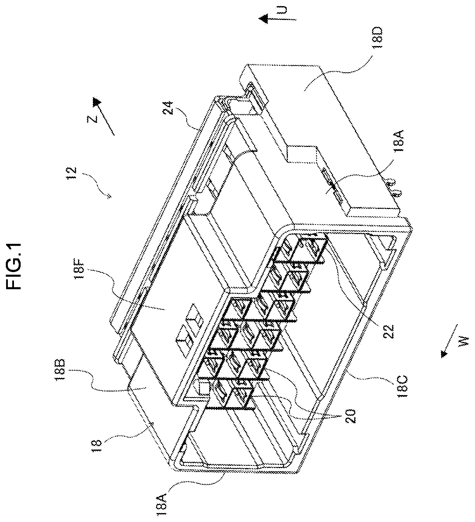
As illustrated in , the board connector 12 is fixed to a circuit board (not illustrated). Further, a cable connector (not illustrated) which is a mating connector is connected to the board connector 12 . A direction in which the board connector 12 and the cable connector (not illustrated) are connected is referred to as a connection axis direction. In addition, a direction orthogonal to the connection axis direction and in which a plurality of terminal units 20 and 22 to be described below are arranged is referred to as a width direction. Further, a direction orthogonal to the connection axis direction and the width direction is referred to as a vertical direction. One side in the connection axis direction is indicated by an arrow Z, one side in the width direction is indicated by an arrow W, and an upper side in the vertical direction is indicated by an arrow U.
As illustrated in , 2 , and 3 , the board connector 12 includes a terminal unit housing 18 , the plurality of terminal units 20 and 22 housed in the terminal unit housing 18 , and a coupling member 24 locked to the terminal unit housing 18 .
As illustrated in , the terminal unit housing 18 is formed in a rectangular frame shape. The terminal unit housing 18 includes a pair of side wall portions 18 A arranged at an interval in the width direction, an upper wall portion 18 B connecting upper ends of the pair of side wall portions 18 A in the width direction, and a lower wall portion 18 C connecting lower ends of the pair of side wall portions 18 A in the width direction.
A portion of each of the pair of side wall portions 18 A on one side in the connection axis direction is a separation restricting portion 18 D extending toward one side in the connection axis direction with respect to the upper wall portion 18 B and the lower wall portion 18 C. A locking groove 18 E in which the coupling member 24 described below is locked is formed in the separation restricting portion 18 D of each of the pair of side wall portions 18 A.
A first holding portion 18 F is formed at a central portion of the upper wall portion 18 B in the width direction. An end portion of the upper wall portion 18 B on one side in the connection axis direction is an upper locking portion 18 G to which upper portions of the plurality of terminal units 20 and 22 described below are locked. The upper locking portion 18 G includes an upper substrate portion 18 H extending in the width direction with the vertical direction as a thickness direction, and an upper flange portion 18 J bent and extending upward from an end of the upper substrate portion 18 H on one side in the connection axis direction. In the upper locking portion 18 G, a plurality of upper locking grooves 18 K arranged at intervals in the width direction are formed in the connection axis direction. The number of upper locking grooves 18 K is equal to the number of terminal units 20 and 22 described below. That is, in the present embodiment, seven upper locking grooves 18 K are formed in the upper locking portion 18 G. In addition, the upper locking groove 18 K is formed in such a way as to penetrate the upper substrate portion 18 H, and is formed in such a way that a lower side of the upper locking groove 18 K is opened at a lower portion of the upper flange portion 18 J.
An end portion of the lower wall portion 18 C on one side in the connection axis direction is a lower locking portion 18 L to which lower portions of the plurality of terminal units 20 and 22 described below are locked. The lower locking portion 18 L includes a lower flange portion 18 M bent and extending upward from an end of the lower wall portion 18 C on one side in the connection axis direction. In the lower flange portion 18 M, a plurality of lower locking grooves 18 N arranged at intervals in the width direction are formed in the connection axis direction. The number of lower locking grooves 18 N is equal to the number of terminal units 20 and 22 described below. That is, in the embodiment, seven lower locking grooves 18 N are formed in the lower flange portion 18 M. Further, the lower locking groove 18 N is formed in such a way that an upper side of the lower locking groove 18 N is opened at an upper portion of the lower flange portion 18 M.
As illustrated in , 7 , and 8 , the board connector 12 of the embodiment includes five terminal units 20 and two terminal units 22 . Here, as illustrated in , the configurations of the terminal unit 20 and the terminal unit 22 are similar to each other except that the number of inner terminals 26 is different. Therefore, hereinafter, the configuration of the terminal unit 22 will be described, and a description of the configuration of the terminal unit 20 will be omitted. In the terminal unit 20 , members and portions corresponding to the terminal unit 22 are denoted by the same reference signs as those of the members and portions corresponding to the terminal unit 22 .
As illustrated in , 9 , and 10 , the terminal unit 22 includes two pairs of inner terminals 26 as terminals and an outer terminal 28 covering the two pairs of inner terminals 26 . In addition, the terminal unit 22 includes a terminal body 30 as a dielectric portion.
The two pairs of inner terminals 26 are formed using a conductive metal material. A detailed configuration of the two pairs of inner terminals 26 will be described below.
As illustrated in , the outer terminal 28 includes one first terminal forming plate 34 formed of a metal plate, and two second terminal forming plates 36 formed of a metal plate and arranged on the other side in the width direction with respect to the first terminal forming plate 34 .
The first terminal forming plate 34 is formed by bending a metal plate cut into a predetermined shape. The first terminal forming plate 34 includes a rectangular first main plate portion 34 A extending in the vertical direction and the connection axis direction with the width direction as the thickness direction, and a rectangular terminal-side extending portion 34 B extending from an end of the first main plate portion 34 A on the other side in the connection axis direction toward the other side in the connection axis direction. A step portion 34 C having a height difference in the width direction is formed at a boundary between the first main plate portion 34 A and the terminal-side extending portion 34 B. Accordingly, the terminal-side extending portion 34 B is offset to one side in the width direction with respect to the first main plate portion 34 A. In addition, the first terminal forming plate 34 includes a connection piece portion 34 G which protrudes from the first main plate portion 34 A and is connected to the circuit board (not illustrated).
One of the second terminal forming plates 36 is formed by bending a metal plate cut into a predetermined shape. This second terminal formation plate 36 includes a second main plate portion 36 A extending in the vertical direction and the connection axis direction with the width direction as the thickness direction. The second main plate portion 36 A has a shape corresponding to a pair of inner terminals 26 of the two pairs of inner terminals 26 as viewed in the width direction. The second terminal forming plate 36 includes a plurality of second side plate portions 36 B extending from ends of the second main plate portion 36 A toward the first main plate portion 34 A of the first terminal forming plate 34 . Further, the second terminal forming plate 36 includes a connection piece portion 36 C which protrudes from the second main plate portion 36 A and is connected to the circuit board (not illustrated).
The other one of the second terminal forming plates 36 is formed by bending a metal plate cut into a predetermined shape smaller than the one second terminal forming plate 36 . This second terminal forming plate 36 includes a second main plate portion 36 A and a plurality of second side plate portions 36 B respectively corresponding to the second main plate portion 36 A and the plurality of second side plate portions 36 B of the one second terminal forming plate 36 . The second main plate portion 36 A of the other second terminal forming plate 36 has a shape corresponding to the remaining pair of inner terminals 26 of the two pairs of inner terminals 26 as viewed in the width direction.
Then, as illustrated in , 9 , and 10 , a terminal-side cover portion 38 that covers most of a pair of inner terminals 26 of the two pairs of inner terminals 26 is formed by the first terminal forming plate 34 and the one second terminal forming plate 36 . Further, the first terminal forming plate 34 and the other second terminal forming plate 36 form the terminal-side cover portion 38 that covers most of the remaining pair of inner terminals 26 of the two pairs of inner terminals 26 .
As illustrated in , 10 , 11 , and 12 , the terminal body 30 is formed in a rectangular box shape using a resin material. In the terminal body 30 , two inner terminal support recesses 30 A opened on the other side in the width direction are formed. Bottom portions of the two inner terminal support recesses 30 A are terminal support portions 30 B that respectively support the two pairs of inner terminals 26 described in detail below. The second main plate portion 36 A and the second side plate portions 36 B of the one second terminal forming plate 36 are arranged in one of the inner terminal support recesses 30 A. Further, the second main plate portion 36 A and the second side plate portions 36 B of the other second terminal forming plate 36 are arranged in the other one of the inner terminal support recesses 30 A.
In addition, the terminal body 30 includes three fitted portions 30 D having holes opened on the other side in the width direction. In addition, the terminal body 30 includes three fitting portions 30 E which are protruding portions protruding toward one side in the width direction. As illustrated in , 9 , 10 , 11 , and 12 , the fitting portion 30 E of the terminal body 30 of one terminal unit 20 or 22 and the fitted portion 30 D of the terminal body 30 of the other terminal unit 20 or 22 are fitted to each other, the one terminal unit 20 or 22 and the other terminal unit 20 or 22 being adjacent to each other in the width direction, so that relative displacement of the one terminal unit 20 or 22 in the connection axis direction and the vertical direction with respect to the other terminal unit 20 or 22 is restricted. Openings through which the three fitting portions 30 E are inserted are formed in the first main plate portion 34 A of the first terminal forming plate 34 .
An upper locking protrusion 30 F protruding upward is formed in the connection axis direction at a central portion of an upper portion of the terminal body 30 in the width direction. A lower locking protrusion 30 G protruding downward is formed in the connection axis direction at a central portion of a lower portion of the terminal body 30 in the width direction. Further, a coupling member locking portion 30 H to which the coupling member 24 described below is locked is formed in the vertical direction at a central portion of an end portion of the terminal body 30 in the connection axis direction, in the width direction.
As illustrated in , the coupling member 24 is formed using a metal plate. A plurality of locking grooves 24 A into which the coupling member locking portions 30 H of the terminal body 30 are fitted are formed in a lower portion of the coupling member 24 . The plurality of locking grooves 24 A are arranged at intervals in the width direction. The number of locking grooves 24 A is equal to the number of terminal units 20 and 22 . That is, in the embodiment, seven locking grooves 24 A are formed in the coupling member 24 . Both end portions of the coupling member 24 in the width direction are housing locking portions 24 B locked to the locking grooves 18 E formed in the separation restricting portions 18 D of the terminal unit housing 18 .
As illustrated in to 12 , the board connector 12 of the embodiment is assembled by the following procedure.
First, the plurality of terminal units 20 and 22 are arranged in the width direction in a state where adjacent terminal units are in contact with each other. At this time, the fitting portion 30 E of the terminal body 30 of the terminal unit 20 or 22 is fitted to the fitted portion 30 D of the terminal body 30 of the other adjacent terminal unit 20 or 22 . In the embodiment, a spacer 41 is provided on one side in the width direction. The fitting portion 30 E of the terminal body 30 of the terminal unit 20 arranged at an end portion on one side in the width direction is fitted to the spacer 41 .
Next, the plurality of terminal units 20 and 22 arranged in the width direction are assembled into the terminal unit housing 18 . That is, the plurality of terminal units 20 and 22 arranged in the width direction are inserted into the terminal unit housing 18 by moving the plurality of terminal units 20 and 22 arranged in the width direction toward the other side in a connection direction. At this time, the upper locking protrusion 30 F of the terminal body 30 of each of the terminal units 20 and 22 is arranged in the upper locking groove 18 K formed in the terminal unit housing 18 , and the lower locking protrusion 30 G of the terminal body 30 of each of the terminal units 20 and 22 is arranged in the lower locking groove 18 N formed in the terminal unit housing 18 . Then, the upper locking protrusion 30 F of the terminal body 30 of each of the terminal units 20 and 22 gets over the upper locking portion 18 G of the terminal unit housing 18 and is locked to the upper locking portion 18 G. The lower locking protrusion 30 G of the terminal body 30 of each of the terminal units 20 and 22 gets over the lower locking portion 18 L of the terminal unit housing 18 and is locked to the lower locking portion 18 L. As a result, the terminal units 20 and 22 are assembled into the terminal unit housing 18 .
Next, the housing locking portion 24 B of the coupling member 24 is locked to the locking groove 18 E formed in the separation restricting portion 18 D of the terminal unit housing 18 , and the coupling member locking portion 30 H of the terminal body 30 of each of the terminal units 20 and 22 is locked to each locking groove 24 A of the coupling member 24 .
Through the above steps, the board connector 12 is assembled.
Next, the detailed configurations of the two pairs of inner terminals 26 and the terminal body 30 , which are main configurations of the embodiment, will be described.
As illustrated in , a pair of inner terminals 26 (a first inner terminal 26 T 1 and a second inner terminal 26 T 2 described below) of the two pairs of inner terminals 26 is supported by the terminal support portion 30 B of the one inner terminal support recess 30 A formed on an upper side of the terminal body 30 and one side in the connection axis direction. The terminal support portion 30 B of the other inner terminal support recess 30 A formed on a lower side of the terminal body 30 and on the other side in the connection axis direction supports the remaining pair of inner terminals 26 (a third inner terminal 26 T 3 and a fourth inner terminal 26 T 4 described below) of the two pairs of inner terminals 26 .
These inner terminals 26 are terminals through which a differential signal is transmitted. These inner terminals 26 each include a fitting-side extending portion 26 A as a first connecting portion that is one side end portion of the inner terminal 26 , a board-side extending portion 26 B as a second connecting portion that is the other side end portion of the inner terminal 26 , and an intermediate extending portion 26 C as a coupling portion coupling the fitting-side extending portion 26 A and the board-side extending portion 26 B to each other. The fitting-side extending portion 26 A extends in the connection axis direction, and is a portion to which a terminal of a wiring connector (not illustrated) is fitted. The board-side extending portion 26 B extends in the vertical direction and is a portion connected to the circuit board (not illustrated).
Here, the inner terminal 26 including the fitting-side extending portion 26 A arranged on the uppermost side is referred to as a first inner terminal 26 T 1 . The inner terminal 26 arranged adjacent to the first inner terminal 26 T 1 is referred to as a second inner terminal 26 T 2 . Further, the inner terminal 26 including the fitting-side extending portion 26 A arranged below the fitting-side extending portion 26 A of the second inner terminal 26 T 2 is referred to as a third inner terminal 26 T 3 . The inner terminal 26 arranged adjacent to the third inner terminal 26 T 3 is referred to as a fourth inner terminal 26 T 4 .
The intermediate extending portion 26 C of the first inner terminal 26 T 1 includes a first intermediate portion T 11 extending from the fitting-side extending portion 26 A toward one side in the connection axis direction, and a second intermediate portion T 12 extending obliquely downward from an end of the first intermediate portion T 11 on a side opposite to the fitting-side extending portion 26 A toward one side in a fitting direction. The intermediate extending portion 26 C of the first inner terminal 26 T 1 includes a third intermediate portion T 13 extending downward from an end of the second intermediate portion T 12 on a side opposite to the first intermediate portion T 11 and having a lower end connected to the board-side extending portion 26 B.
The intermediate extending portion 26 C of the second inner terminal 26 T 2 includes a first intermediate portion T 21 extending from the fitting-side extending portion 26 A toward one side in the connection axis direction, and a second intermediate portion T 22 extending obliquely upward from an end of the first intermediate portion T 21 on a side opposite to the fitting-side extending portion 26 A toward one side in the fitting direction. The intermediate extending portion 26 C of the second inner terminal 26 T 2 includes a third intermediate portion T 23 extending from an end of the second intermediate portion T 22 on a side opposite to the first intermediate portion T 21 toward one side in the connection axis direction, and a fourth intermediate portion T 24 extending obliquely downward from an end of the third intermediate portion T 23 on a side opposite to the second intermediate portion T 22 toward one side in the fitting direction. Further, the intermediate extending portion 26 C of the second inner terminal 26 T 2 includes a fifth intermediate portion T 25 extending downward from an end of the fourth intermediate portion T 24 on a side opposite to the third intermediate portion T 23 , and a sixth intermediate portion T 26 extending obliquely toward the other side in the connection axis direction from an end of the fifth intermediate portion T 25 on a side opposite to the fourth intermediate portion T 24 toward the lower side. The intermediate extending portion 26 C of the second inner terminal 26 T 2 includes a seventh intermediate portion T 27 extending downward from an end of the sixth intermediate portion T 26 on a side opposite to the fifth intermediate portion T 25 and having a lower end connected to the board-side extending portion 26 B.
In the embodiment, the first intermediate portion T 11 of the intermediate extending portion 26 C of the first inner terminal 26 T 1 and the first intermediate portion T 21 and the third intermediate portion T 23 of the intermediate extending portion 26 C of the second inner terminal 26 T 2 extend in parallel. In addition, the second intermediate portion T 12 of the intermediate extending portion 26 C of the first inner terminal 26 T 1 and the fourth intermediate portion T 24 of the intermediate extending portion 26 C of the second inner terminal 26 T 2 extend in parallel. Further, the third intermediate portion T 13 of the intermediate extending portion 26 C of the first inner terminal 26 T 1 and the fifth intermediate portion T 25 and the seventh intermediate portion T 27 of the intermediate extending portion 26 C of the second inner terminal 26 T 2 extend in parallel.
Here, an spacing between the fitting-side extending portion 26 A of the first inner terminal 26 T 1 and the fitting-side extending portion 26 A of the second inner terminal 26 T 2 is defined as D 1 . An spacing between the board-side extending portion 26 B of the first inner terminal 26 T 1 and the board-side extending portion 26 B of the second inner terminal 26 T 2 is defined as D 2 . Further, an spacing between the second intermediate portion T 12 of the intermediate extending portion 26 C of the first inner terminal 26 T 1 and the fourth intermediate portion T 24 of the intermediate extending portion 26 C of the second inner terminal 26 T 2 is defined as D 3 . In the embodiment, a path of the intermediate extending portion 26 C of the second inner terminal 26 T 2 is set in such a way that the interval D 3 is smaller than the interval D 1 and the interval D 2 . As a result, an electrical length of the intermediate extending portion 26 C of the second inner terminal 26 T 2 is brought close to an electrical length of the intermediate extending portion 26 C of the first inner terminal 26 T 1 .
The intermediate extending portion 26 C of the third inner terminal 26 T 3 includes a first intermediate portion T 31 extending from the fitting-side extending portion 26 A toward one side in the connection axis direction, and a second intermediate portion T 32 extending obliquely downward from an end of the first intermediate portion T 31 on a side opposite to the fitting-side extending portion 26 A toward one side in a fitting direction. The intermediate extending portion 26 C of the third inner terminal 26 T 3 includes a third intermediate portion T 33 extending downward from an end of the second intermediate portion T 32 opposite to the first intermediate portion T 31 and having a lower end connected to the board-side extending portion 26 B.
The intermediate extending portion 26 C of the fourth inner terminal 26 T 4 includes a first intermediate portion T 41 extending from the fitting-side extending portion 26 A toward one side in the connection axis direction, and a second intermediate portion T 42 extending obliquely upward from an end of the first intermediate portion T 41 on a side opposite to the fitting-side extending portion 26 A toward one side in the fitting direction. The intermediate extending portion 26 C of the fourth inner terminal 26 T 4 includes a third intermediate portion T 43 extending from an end of the second intermediate portion T 42 opposite to the first intermediate portion T 41 toward one side in the connection axis direction, and a fourth intermediate portion T 44 extending obliquely downward from an end of the third intermediate portion T 43 opposite to the second intermediate portion T 42 toward one side in the fitting direction. Further, the intermediate extending portion 26 C of the fourth inner terminal 26 T 4 includes a fifth intermediate portion T 45 extending downward from an end of the fourth intermediate portion T 44 on a side opposite to the third intermediate portion T 43 , and a sixth intermediate portion T 46 extending obliquely toward the other side in the connection axis direction from an end of the fifth intermediate portion T 45 on a side opposite to the fourth intermediate portion T 44 toward the lower side. The intermediate extending portion 26 C of the fourth inner terminal 26 T 4 includes a seventh intermediate portion T 47 extending downward from an end of the sixth intermediate portion T 46 opposite to the fifth intermediate portion T 45 and having a lower end connected to the board-side extending portion 26 B.
In the embodiment, the first intermediate portion T 31 of the intermediate extending portion 26 C of the third inner terminal 26 T 3 and the first intermediate portion T 41 and the third intermediate portion T 43 of the intermediate extending portion 26 C of the fourth inner terminal 26 T 4 extend in parallel. In addition, the second intermediate portion T 32 of the intermediate extending portion 26 C of the third inner terminal 26 T 3 and the fourth intermediate portion T 44 of the intermediate extending portion 26 C of the fourth inner terminal 26 T 4 extend in parallel. Further, the third intermediate portion T 33 of the intermediate extending portion 26 C of the third inner terminal 26 T 3 and the fifth intermediate portion T 45 and the seventh intermediate portion T 47 of the intermediate extending portion 26 C of the fourth inner terminal 26 T 4 extend in parallel.
Here, an spacing between the fitting-side extending portion 26 A of the third inner terminal 26 T 3 and the fitting-side extending portion 26 A of the fourth inner terminal 26 T 4 is defined as D 1 . An spacing between the board-side extending portion 26 B of the third inner terminal 26 T 3 and the board-side extending portion 26 B of the fourth inner terminal 26 T 4 is defined as D 2 . Further, an spacing between the second intermediate portion T 32 of the intermediate extending portion 26 C of the third inner terminal 26 T 3 and the fourth intermediate portion T 44 of the intermediate extending portion 26 C of the fourth inner terminal 26 T 4 is defined as D 3 . In the embodiment, a path of the intermediate extending portion 26 C of the fourth inner terminal 26 T 4 is set in such a way that the interval D 3 is smaller than the interval D 1 and the interval D 2 . As a result, an electrical length of the intermediate extending portion 26 C of the fourth inner terminal 26 T 4 is brought close to an electrical length of the intermediate extending portion 26 C of the third inner terminal 26 T 3 .
As illustrated in , the intermediate extending portion 26 C of each of the first inner terminal 26 T 1 , the second inner terminal 26 T 2 , the third inner terminal 26 T 3 , and the fourth inner terminal 26 T 4 described above is partially embedded in the terminal support portion 30 B of the inner terminal support recess 30 A. As a result, the first inner terminal 26 T 1 , the second inner terminal 26 T 2 , the third inner terminal 26 T 3 , and the fourth inner terminal 26 T 4 are held by the terminal body 30 .
Here, in the embodiment, a low-dielectric constant portion 70 is interposed between the second intermediate portion T 12 of the intermediate extending portion 26 C of the first inner terminal 26 T 1 and the fourth intermediate portion T 24 of the intermediate extending portion 26 C of the second inner terminal 26 T 2 . The low-dielectric constant portion 70 is a portion set to have a lower relative dielectric constant than a resin material forming the terminal body 30 . The low-dielectric constant portion 70 of the embodiment is a gap formed between the second intermediate portion T 12 of the intermediate extending portion 26 C of the first inner terminal 26 T 1 and the fourth intermediate portion T 24 of the intermediate extending portion 26 C of the second inner terminal 26 T 2 . Only air exists in the gap which is the low-dielectric constant portion 70 , and a solid such as a part of the terminal body 30 does not exist. In a state where the terminal body 30 is viewed in the width direction, a rectangular opening 30 J is formed at a position corresponding to the low-dielectric constant portion 70 in the terminal support portion 30 B. The opening 30 J penetrates the terminal support portion 30 B in the width direction.
A low-dielectric constant portion 72 is interposed between the second intermediate portion T 32 of the intermediate extending portion 26 C of the third inner terminal 26 T 3 and the fourth intermediate portion T 44 of the intermediate extending portion 26 C of the fourth inner terminal 26 T 4 . The low-dielectric constant portion 72 is the same gap as the low-dielectric constant portion 70 interposed between the second intermediate portion T 12 of the intermediate extending portion 26 C of the first inner terminal 26 T 1 and the fourth intermediate portion T 24 of the intermediate extending portion 26 C of the second inner terminal 26 T 2 . Only air exists in the gap which is the low-dielectric constant portion 72 , and a solid such as a part of the terminal body 30 does not exist. In a state where the terminal body 30 is viewed in the width direction, a rectangular opening 30 K is formed at a position corresponding to the low-dielectric constant portion 72 in the terminal support portion 30 B. The opening 30 K penetrates the terminal support portion 30 B in the width direction.
Further, in the embodiment, a side of the fourth intermediate portion T 24 of the intermediate extending portion 26 C of the second inner terminal 26 T 2 that is opposite to the low-dielectric constant portion 70 is covered with a part of the terminal support portion 30 B (hereinafter referred to as “cover portion 30 L”) in the width direction. The cover portion 30 L is formed in a rectangular shape that covers, in the width direction, the side of the fourth intermediate portion T 24 that is opposite to the low-dielectric constant portion 70 and a central portion of the fourth intermediate portion T 24 in a longitudinal direction. A side of the fourth intermediate portion T 44 of the intermediate extending portion 26 C of the fourth inner terminal 26 T 4 that is opposite to the low-dielectric constant portion 72 is covered with a part of the terminal support portion 30 B (hereinafter referred to as “cover portion 30 M”) in the width direction. The cover portion 30 M is formed in a rectangular shape that covers, in the width direction, the side of the fourth intermediate portion T 44 that is opposite to the low-dielectric constant portion 72 and a central portion of the fourth intermediate portion T 44 in the longitudinal direction.
In the embodiment, a side of the second intermediate portion T 12 of the intermediate extending portion 26 C of the first inner terminal 26 T 1 that is opposite to the low-dielectric constant portion 70 and a central portion of the second intermediate portion T 12 in the longitudinal direction bulge only toward a side opposite to the low-dielectric constant portion 70 . As a result, a width W 1 of the central portion of the second intermediate portion T 12 in the longitudinal direction is larger than a width W 2 of each of both end portions of the second intermediate portion T 12 in the longitudinal direction. In addition, in the embodiment, a side of the second intermediate portion T 32 of the intermediate extending portion 26 C of the third inner terminal 26 T 3 that is opposite to the low-dielectric constant portion 72 and a central portion of the second intermediate portion T 32 in the longitudinal direction bulge only toward a side opposite to the low-dielectric constant portion 72 . As a result, a width W 1 of the central portion of the second intermediate portion T 32 in the longitudinal direction is larger than a width W 2 of each of both end portions of the second intermediate portion T 32 in the longitudinal direction.
Actions and Effects of Embodiment
Next, actions and effects of the embodiment will be described.
As illustrated in to 3 and to 13 , the board connector 12 of the embodiment includes the plurality of terminal units 20 and 22 each including the inner terminals 26 , the outer terminal 28 , and the terminal body 30 . The plurality of terminal units 20 and 22 are arranged side by side in the width direction in a state where adjacent terminal units are in contact with each other. As described above, with the configuration of the board connector 12 of the embodiment, it is possible to facilitate variable deployment of the board connector 12 corresponding to variations of electric wire connectors (not illustrated) by setting the number of terminal units 20 and 22 if appropriate.
In addition, the board connector 12 of the embodiment includes the terminal unit 22 having the above-described configuration. In the terminal unit 22 , a differential signal is transmitted between the wiring connector and the circuit board via the two pairs of inner terminals 26 (the first inner terminal 26 T 1 and the second inner terminal 26 T 2 , and the third inner terminal 26 T 3 and the fourth inner terminal 26 T 4 ).
Here, the two pairs of inner terminals 26 (the first inner terminal 26 T 1 and the second inner terminal 26 T 2 , and the third inner terminal 26 T 3 and the fourth inner terminal 26 T 4 ) are held by the terminal body 30 formed using a resin material. The low-dielectric constant portion 70 having a lower relative dielectric constant than that of the resin material forming the terminal body 30 is interposed between the second intermediate portion T 12 of the intermediate extending portion 26 C of the first inner terminal 26 T 1 and the fourth intermediate portion T 24 of the intermediate extending portion 26 C of the second inner terminal 26 T 2 . Further, the low-dielectric constant portion 72 having a lower relative dielectric constant than that of the resin material forming the terminal body 30 is interposed between the second intermediate portion T 32 of the intermediate extending portion 26 C of the third inner terminal 26 T 3 and the fourth intermediate portion T 44 of the intermediate extending portion 26 C of the fourth inner terminal 26 T 4 . As a result, a decrease in impedance can be suppressed as compared with a configuration in which the resin material forming the terminal body 30 is interposed between portions corresponding to the low-dielectric constant portions 70 and 72 .
In addition, the interval D 3 between the second intermediate portion T 12 of the intermediate extending portion 26 C of the first inner terminal 26 T 1 and the fourth intermediate portion T 24 of the intermediate extending portion 26 C of the second inner terminal 26 T 2 is set to be smaller than the interval D 1 between the fitting-side extending portion 26 A of the first inner terminal 26 T 1 and the fitting-side extending portion 26 A of the second inner terminal 26 T 2 and the interval D 2 between the board-side extending portion 26 B of the first inner terminal 26 T 1 and the board-side extending portion 26 B of the second inner terminal 26 T 2 . In addition, the interval D 3 between the second intermediate portion T 32 of the intermediate extending portion 26 C of the third inner terminal 26 T 3 and the fourth intermediate portion T 44 of the intermediate extending portion 26 C of the fourth inner terminal 26 T 4 is set to be smaller than the interval D 1 between the fitting-side extending portion 26 A of the third inner terminal 26 T 3 and the fitting-side extending portion 26 A of the fourth inner terminal 26 T 4 and the interval D 2 between the board-side extending portion 26 B of the third inner terminal 26 T 3 and the board-side extending portion 26 B of the fourth inner terminal 26 T 4 . As a result, it is possible to reduce the skew of a differential signal as compared with a configuration in which the intervals D 1 , D 2 , and D 3 are set outside the above range. In addition, as compared with a configuration in which the intervals D 1 , D 2 , and D 3 are set outside the above range, a common mode impedance at the intermediate extending portion 26 C of the first inner terminal 26 T 1 and the intermediate extending portion 26 C of the second inner terminal 26 T 2 can be increased, and a common mode impedance at the intermediate extending portion 26 C of the third inner terminal 26 T 3 and the intermediate extending portion 26 C of the fourth inner terminal 26 T 4 can be increased. As a result, common mode noise that has occurred is less likely to propagate beyond between the intermediate extending portion 26 C of the first inner terminal 26 T 1 and the intermediate extending portion 26 C of the second inner terminal 26 T 2 and between the intermediate extending portion 26 C of the third inner terminal 26 T 3 and the intermediate extending portion 26 C of the fourth inner terminal 26 T 4 , and as a result, propagation of the common mode noise can be suppressed. As described above, with the board connector 12 of the embodiment, it is possible to achieve both a countermeasure against the common mode noise and impedance matching.
In the terminal unit 22 of the embodiment, the intermediate extending portion 26 C of each of the first inner terminal 26 T 1 , the second inner terminal 26 T 2 , the third inner terminal 26 T 3 , and the fourth inner terminal 26 T 4 described above is partially embedded in the terminal support portion 30 B of the inner terminal support recess 30 A. As a result, the first inner terminal 26 T 1 , the second inner terminal 26 T 2 , the third inner terminal 26 T 3 , and the fourth inner terminal 26 T 4 are held by the terminal body 30 . In addition, in the terminal unit 22 of the embodiment, the above-described low-dielectric constant portions 70 and 72 are gaps. In this configuration, for example, the first inner terminal 26 T 1 , the second inner terminal 26 T 2 , the third inner terminal 26 T 3 , and the fourth inner terminal 26 T 4 can be held by the terminal body 30 by insert molding. In addition, a portion where a part of the metal mold is positioned can be the gap (the low-dielectric constant portion 70 or 72 ) by opening the metal mold for insert molding. Thus, the productivity of the connector can be improved. Hereinafter, a process of the insert molding will be briefly described.
illustrates the first inner terminal 26 T 1 , the second inner terminal 26 T 2 , the third inner terminal 26 T 3 , and the fourth inner terminal 26 T 4 in the middle of manufacturing. In the stage illustrated in , the board-side extending portion 26 B of each of the first inner terminal 26 T 1 , the second inner terminal 26 T 2 , the third inner terminal 26 T 3 , and the fourth inner terminal 26 T 4 is connected via a first connecting portion 74 A. The fourth intermediate portion T 24 of the intermediate extending portion 26 C of the second inner terminal 26 T 2 and the second intermediate portion T 32 of the intermediate extending portion 26 C of the third inner terminal 26 T 3 are connected via a second connecting portion 74 B. Further, the first intermediate portion T 11 of the intermediate extending portion 26 C of the first inner terminal 26 T 1 and the first intermediate portion T 21 of the intermediate extending portion 26 C of the second inner terminal 26 T 2 are connected via a third connecting portion 74 C.
illustrates the first inner terminal 26 T 1 , the second inner terminal 26 T 2 , the third inner terminal 26 T 3 , and the fourth inner terminal 26 T 4 in a process subsequent to the process illustrated in . As illustrated in , in this process, most of the second connecting portion 74 B and the third connecting portion 74 C are removed. Then, in the state illustrated in , the first inner terminal 26 T 1 , the second inner terminal 26 T 2 , the third inner terminal 26 T 3 , and the fourth inner terminal 26 T 4 are set in a mold. Next, the inside of the mold is filled with a resin material.
Next, as illustrated in , the terminal body 30 in a state where the first inner terminal 26 T 1 , the second inner terminal 26 T 2 , the third inner terminal 26 T 3 , and the fourth inner terminal 26 T 4 are held is formed by opening the mold. After this process, the first connecting portion 74 A is removed.
As illustrated in , in the terminal unit 22 of the embodiment, the cover portion 30 L is a part of the terminal support portion 30 B and covers, in the width direction, the side of the fourth intermediate portion T 24 that is opposite to the low-dielectric constant portion 70 and the central portion of the fourth intermediate portion T 24 in the longitudinal direction. In this configuration, it is possible to suppress an increase in skew of a differential signal due to shortening of the electrical length of the fourth intermediate portion T 24 as compared with a configuration in which the entire fourth intermediate portion T 24 is covered with the resin material forming the terminal body 30 . In addition, in the terminal unit 22 of the embodiment, the cover portion 30 M is a part of the terminal support portion 30 B and covers, in the width direction, the side of the fourth intermediate portion T 44 that is opposite to the low-dielectric constant portion 72 and the central portion of the fourth intermediate portion T 44 in the longitudinal direction. In this configuration, it is possible to suppress an increase in skew of a differential signal due to shortening of the electrical length of the fourth intermediate portion T 44 as compared with a configuration in which the entire fourth intermediate portion T 44 is covered with the resin material forming the terminal body 30 .
As illustrated in , the width W 1 of the central portion of the second intermediate portion T 12 of the intermediate extending portion 26 C of the first inner terminal 26 T 1 in the longitudinal direction is larger than the width W 2 of each of both end portions of the second intermediate portion T 12 in the longitudinal direction. As a result, the electrical length of the second intermediate portion T 12 can be shortened as compared with a configuration in which the second intermediate portion T 12 has a uniform width W 2 . In addition, the second intermediate portion T 12 of the intermediate extending portion 26 C of the first inner terminal 26 T 1 and the fourth intermediate portion T 24 of the intermediate extending portion 26 C of the second inner terminal 26 T 2 can be arranged close to each other by adopting a configuration in which the side of the second intermediate portion T 12 that is opposite to the low-dielectric constant portion 70 and the central portion of the second intermediate portion T 12 in the longitudinal direction bulge only toward the side opposite to the low-dielectric constant portion 70 . In addition, the width W 1 of the central portion of the second intermediate portion T 32 of the intermediate extending portion 26 C of the third inner terminal 26 T 3 in the longitudinal direction is larger than the width W 2 of each of both end portions of the second intermediate portion T 32 in the longitudinal direction. As a result, the electrical length of the second intermediate portion T 32 can be shortened as compared with a configuration in which the second intermediate portion T 32 has a uniform width W 2 . In addition, the second intermediate portion T 32 of the intermediate extending portion 26 C of the third inner terminal 26 T 3 and the fourth intermediate portion T 44 of the intermediate extending portion 26 C of the fourth inner terminal 26 T 4 can be arranged close to each other by adopting a configuration in which the side of the second intermediate portion T 32 that is opposite to the low-dielectric constant portion 72 and the central portion of the second intermediate portion T 32 in the longitudinal direction bulge only toward the side opposite to the low-dielectric constant portion 72 .
In the embodiment, an example has been described in which the width W 1 of the central portion of the second intermediate portion T 12 of the intermediate extending portion 26 C of the first inner terminal 26 T 1 in the longitudinal direction is larger than the width W 2 of each of both end portions of the second intermediate portion T 12 in the longitudinal direction, but the present disclosure is not limited thereto. It is sufficient if the width of the second intermediate portion T 12 of the intermediate extending portion 26 C of the first inner terminal 26 T 1 is set in consideration of a balance between the electrical length of the first inner terminal 26 T 1 and the electrical length of the second inner terminal 26 T 2 if appropriate. In the embodiment, an example has been described in which the width W 1 of the central portion of the second intermediate portion T 32 of the intermediate extending portion 26 C of the third inner terminal 26 T 3 in the longitudinal direction is larger than the width W 2 of each of both end portions of the second intermediate portion T 32 in the longitudinal direction, but the present disclosure is not limited thereto. It is sufficient if the width of the second intermediate portion T 32 of the intermediate extending portion 26 C of the third inner terminal 26 T 3 is set in consideration of a balance between the electrical length of the third inner terminal 26 T 3 and the electrical length of the fourth inner terminal 26 T 4 if appropriate.
In the embodiment, an example has been described in which the cover portions 30 L and 30 M are parts of the terminal support portion 30 B, but the present disclosure is not limited thereto. It is sufficient if whether or not to set parts of the terminal support portion 30 B as the cover portions 30 L and 30 M is determined in consideration of the level of skew of a differential signal if appropriate.
In addition, in the embodiment, an example in which the low-dielectric constant portions 70 and 72 are gaps has been described, but the present disclosure is not limited thereto. For example, a low-dielectric constant portion set to have a lower relative dielectric constant than the resin material forming the terminal body 30 may be interposed at a position corresponding to the low-dielectric constant portions 70 and 72 .
In the embodiment, an example has been described in which the interval D 3 between the second intermediate portion T 12 of the intermediate extending portion 26 C of the first inner terminal 26 T 1 and the fourth intermediate portion T 24 of the intermediate extending portion 26 C of the second inner terminal 26 T 2 is set to be smaller than the interval D 1 between the fitting-side extending portion 26 A of the first inner terminal 26 T 1 and the fitting-side extending portion 26 A of the second inner terminal 26 T 2 and the interval D 2 between the board-side extending portion 26 B of the first inner terminal 26 T 1 and the board-side extending portion 26 B of the second inner terminal 26 T 2 , but the present disclosure is not limited thereto. For example, the interval D 3 between the second intermediate portion T 12 of the intermediate extending portion 26 C of the first inner terminal 26 T 1 and the fourth intermediate portion T 24 of the intermediate extending portion 26 C of the second inner terminal 26 T 2 may be set to be smaller than any one of the interval D 1 between the fitting-side extending portion 26 A of the first inner terminal 26 T 1 and the fitting-side extending portion 26 A of the second inner terminal 26 T 2 and the interval D 2 between the board-side extending portion 26 B of the first inner terminal 26 T 1 and the board-side extending portion 26 B of the second inner terminal 26 T 2 .
Further, in the embodiment, an example has been described in which the interval D 3 between the second intermediate portion T 32 of the intermediate extending portion 26 C of the third inner terminal 26 T 3 and the fourth intermediate portion T 44 of the intermediate extending portion 26 C of the fourth inner terminal 26 T 4 is set to be smaller than the interval D 1 between the fitting-side extending portion 26 A of the third inner terminal 26 T 3 and the fitting-side extending portion 26 A of the fourth inner terminal 26 T 4 and the interval D 2 between the board-side extending portion 26 B of the third inner terminal 26 T 3 and the board-side extending portion 26 B of the fourth inner terminal 26 T 4 , but the present disclosure is not limited thereto. For example, the interval D 3 between the second intermediate portion T 32 of the intermediate extending portion 26 C of the third inner terminal 26 T 3 and the fourth intermediate portion T 44 of the intermediate extending portion 26 C of the fourth inner terminal 26 T 4 may be set to be smaller than any one of the interval D 1 between the fitting-side extending portion 26 A of the third inner terminal 26 T 3 and the fitting-side extending portion 26 A of the fourth inner terminal 26 T 4 and the interval D 2 between the board-side extending portion 26 B of the third inner terminal 26 T 3 and the board-side extending portion 26 B of the fourth inner terminal 26 T 4 .
Although an embodiment of the present disclosure has been described above, the present disclosure is not limited thereto, and it is a matter of course that the present disclosure may be variously modified and implemented without departing from the gist of the present disclosure.
Figures (16)
Citations
This patent cites (25)
- US6183302
- US6293827
- US6361367
- US6371812
- US7131870
- US8172614
- US8540525
- US10581203
- US11563291
- US2002/0168898
- US2014/0248796
- US2014/0273651
- US2021/0066857
- US2023/0144535
- US1531653
- USH11329635
- US2000068006
- US2000260529
- US2003522387
- US2004014800
- US2004274047
- US2011018655
- US2012252904
- US2019136199
- US2021228655