Antenna Module and Communication Device Equipped Therewith
Abstract
An antenna module including dielectric electrodes whose normal directions are different from each other, emitting elements and a ground electrode disposed on the dielectric substrate, and emitting elements disposed on the dielectric substrate. The emitting element is capable of emitting radio waves of a first frequency band. The emitting element is disposed adjacent to the emitting element and is capable of emitting radio waves of a second frequency band higher than the first frequency band. On the dielectric substrate, the emitting element is disposed at a position that is closer to the dielectric substrate than the emitting element is. The distance from the center of the emitting element to an end surface of the ground electrode that is closer to the dielectric substrate is shorter than the distance from the center of the emitting element to an end surface of the ground electrode that is farther from the dielectric substrate.
Claims (20)
1 . An antenna module comprising: a first substrate and a second substrate, whose normal directions are different from each other; a first emitting element capable of emitting radio waves of a first frequency band, the first emitting element being disposed on the first substrate; a second emitting element capable of emitting radio waves of a second frequency band higher than the first frequency band, the second emitting element being disposed adjacent to the first emitting element on the first substrate; a ground electrode disposed on the first substrate so as to face the first emitting element and the second emitting element; and a third emitting element disposed on the second substrate, wherein on the first substrate, the first emitting element is disposed at a position that is closer to the second substrate than the second emitting element is, and a distance from a center of the first emitting element to an end surface of the ground electrode that is closer to the second substrate is shorter than a distance from the center of the first emitting element to an end surface of the ground electrode that is farther from the second substrate.
18 . An antenna module comprising: a first substrate and a second substrate, whose normal directions are different from each other; an emitting element disposed on the first substrate and having a flat plate-like shape; a ground electrode disposed on the first substrate so as to face the fifth emitting element; and another emitting element disposed on the second substrate and having a flat plate-like shape, wherein on the first substrate, a distance from a center of the emitting element to an end surface of the ground electrode that is closer to the second substrate is shorter than a length of a side of an electrode of the emitting element and is shorter than a distance from the center of the emitting element to an end surface of the ground electrode that is farther from the second substrate.
Show 18 dependent claims
2 . The antenna module according to claim 1 , wherein the first emitting element and the second emitting element are planar electrodes having rectangular shapes, and the distance from the center of the first emitting element to the end surface of the ground electrode that is closer to the second substrate is shorter than a length of a side of an electrode of the first emitting element.
3 . The antenna module according to claim 2 , further comprising: a connection member that connects the first substrate and the second substrate.
4 . The antenna module according to claim 3 , wherein each of the first emitting element and the second emitting element includes a plurality of electrodes arranged in a direction along the second substrate.
5 . The antenna module according to claim 4 , wherein the electrodes of the first emitting element and the electrodes of the second emitting element are disposed in an alternating manner in the direction along the second substrate.
6 . The antenna module according to claim 5 , further comprising: a fourth emitting element disposed on the second substrate, wherein the third emitting element is capable of emitting radio waves of the first frequency band, and the fourth emitting element is capable of emitting radio waves of the second frequency band.
7 . The antenna module according to claim 6 , wherein in a case where the second substrate is viewed in a plan view from a normal direction, the third emitting element and the fourth emitting element overlap each other.
8 . The antenna module according to claim 6 , wherein in a case where the second substrate is viewed in a plan view from a normal direction, the third emitting element and the fourth emitting element are disposed adjacent to each other.
9 . The antenna module according to claim 8 , wherein each of the third emitting element and the fourth emitting element includes a plurality of electrodes arranged in a direction along the first substrate.
10 . The antenna module according to claim 9 , wherein the electrodes of the third emitting element and the electrodes of the fourth emitting element are disposed in an alternating manner in the direction along the first substrate.
11 . The antenna module according to claim 1 , further comprising: a power feed circuit that is disposed on the first substrate and is configured to supply a radio frequency signal to each emitting element.
12 . A communication device comprising: the antenna module according to claim 1 .
13 . The antenna module according to claim 1 , further comprising: a connection member that connects the first substrate and the second substrate.
14 . The antenna module according to claim 13 , wherein each of the first emitting element and the second emitting element includes a plurality of electrodes arranged in a direction along the second substrate.
15 . The antenna module according to claim 14 , wherein the electrodes of the first emitting element and the electrodes of the second emitting element are disposed in an alternating manner in the direction along the second substrate.
16 . The antenna module according to claim 15 , further comprising: a fourth emitting element disposed on the second substrate, wherein the third emitting element is capable of emitting radio waves of the first frequency band, and the fourth emitting element is capable of emitting radio waves of the second frequency band.
17 . The antenna module according to claim 16 , wherein in a case where the second substrate is viewed in a plan view from a normal direction, the third emitting element and the fourth emitting element overlap each other, or wherein in a case where the second substrate is viewed in a plan view from a normal direction, the third emitting element and the fourth emitting element are disposed adjacent to each other.
19 . The antenna module according to claim 18 , further comprising: a power feed circuit that is disposed on the first substrate and is configured to supply a radio frequency signal to each emitting element.
20 . A communication device comprising: the antenna module according to claim 18 .
Full Description
Show full text →
CROSS-REFERENCE TO RELATED APPLICATIONS
This is a continuation application of PCT/JP2022/030091, filed on Aug. 5, 2022, designating the United States of America, which is based on and claims priority to Japanese Patent Application No. JP 2021-146761 filed on Sep. 9, 2021. The entire contents of the above-identified applications, including the specifications, drawings and claims, are incorporated herein by reference in their entirety.
TECHNICAL FIELD
The present disclosure relates to an antenna module and a communication device equipped therewith, and more specifically to technology for improving the directivity of an antenna module capable of emitting radio waves in two directions.
BACKGROUND ART
International Publication No. 2020/170722 (Patent Document 1) discloses an antenna module in which emitting elements are disposed on two surfaces of a dielectric substrate having a flat plate-like shape folded into a substantially L shape, the two surfaces having different normal directions. In the antenna module disclosed in Patent Document 1, radio waves can be emitted in different directions from the emitting elements on the respective surfaces of the dielectric substrate.
CITATION LIST
Patent Document
• Patent Document 1: International Publication No. 2020/170722
SUMMARY OF DISCLOSURE
Technical Problem
Antenna modules as described above may be used in mobile communication devices such as, typically, cellular phones or smartphones. In recent years, such mobile communication devices have been communicating using radio waves of a plurality of frequency bands corresponding to different communication standards. In this case, emitting elements corresponding to the individual frequency bands are disposed on the individual surfaces of the dielectric substrate.
In a case where the emitting elements corresponding to different frequency bands are disposed adjacent to each other on the individual surfaces of the dielectric substrate, the emitting elements are disposed in the limited space of the dielectric substrate, which may lead to a state where the emitting elements are disposed at a high density. Depending on the positions of the emitting elements on the dielectric substrate, the directions of emission of radio waves may be tilted toward another dielectric substrate, and this may result in a narrower possible emission range for the entire antenna module.
The present disclosure has been made to solve such a problem, and a purpose of the present disclosure is to increase, for an antenna module capable of emitting radio waves in two different directions, the possible emission range of the entire antenna module.
Solution to Problem
An antenna module according to the present disclosure includes a first substrate and a second substrate, whose normal directions are different from each other, a first emitting element and a second emitting element, which are disposed on the first substrate, a ground electrode, and a third emitting element, which is disposed on the second substrate. The first emitting element is capable of emitting radio waves of a first frequency band. The second emitting element is disposed adjacent to the first emitting element on the first substrate, and is capable of emitting radio waves of a second frequency band higher than the first frequency band. The ground electrode is disposed on the first substrate so as to face the first emitting element and the second emitting element. On the first substrate, the first emitting element is disposed at a position that is closer to the second substrate than the second emitting element is. A distance from a center of the first emitting element to an end surface of the ground electrode that is closer to the second substrate is shorter than a distance from the center of the first emitting element to an end surface of the ground electrode that is farther from the second substrate.
Advantageous Effects of Disclosure
According to an antenna module according to the present disclosure, on a first substrate side, an emitting element for a lower frequency band is disposed at a position that is closer to a second substrate than an emitting element for a higher frequency band is, and furthermore, the distance from the center of the first emitting element to an end surface of a ground electrode that is closer to the second substrate is shorter than the distance from the center of the first emitting element to an end surface of the ground electrode that is farther from the second substrate. With such a configuration, the direction of emission of radio waves from the emitting element for the lower frequency band is tilted toward the opposite direction from the second substrate. This reduces a region where radio waves from the emitting elements disposed on the first substrate and radio waves emitted from the emitting element on the second substrate side overlap each other. This can increase the possible emission range of the entire antenna module.
BRIEF DESCRIPTION OF DRAWINGS
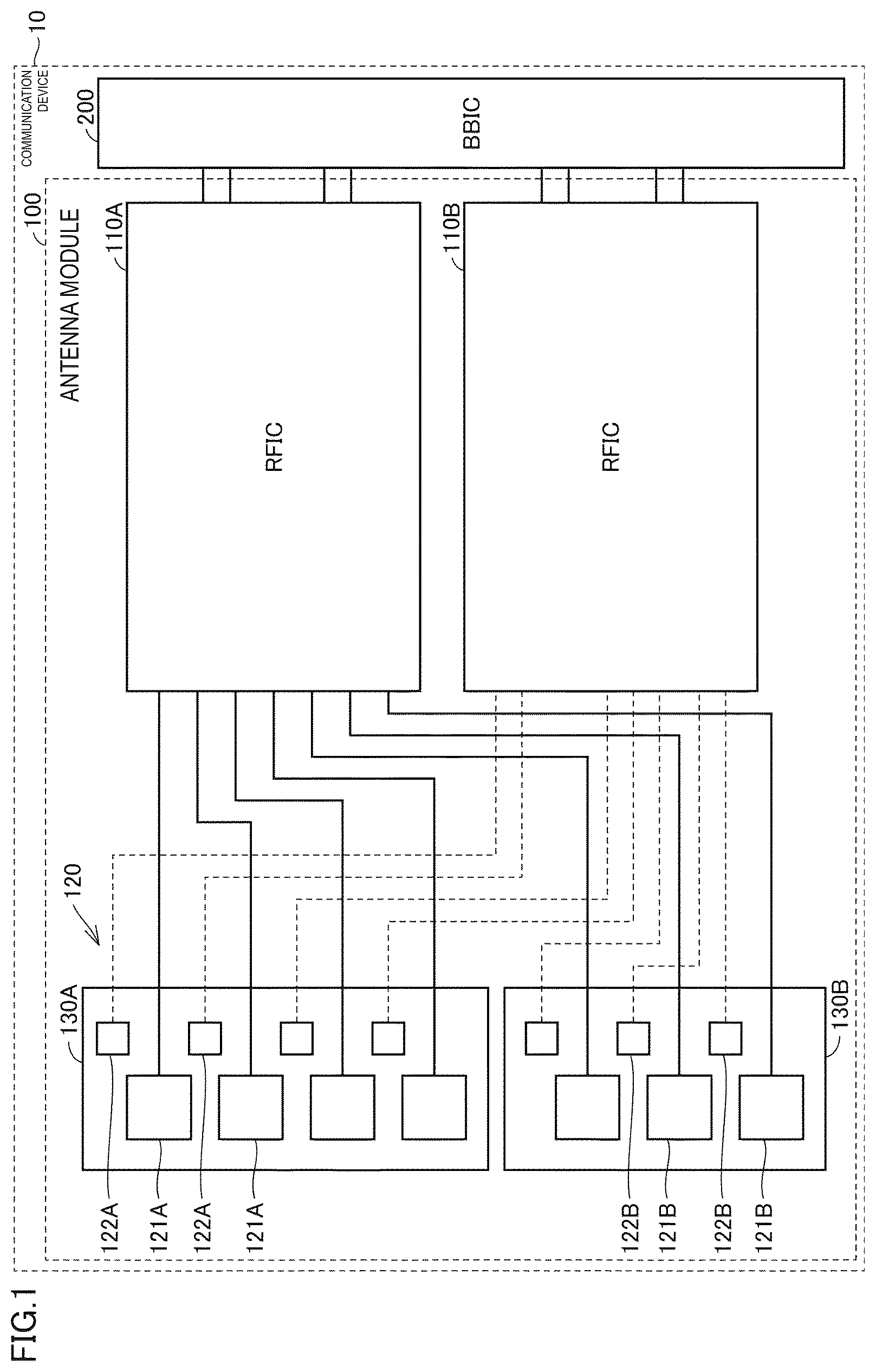
is a block diagram of a communication device to which an antenna module according to an embodiment is applied.
is a diagram for describing a detailed configuration of RFICs of .
is a perspective view of the antenna module according to the embodiment.
is a perspective view of an antenna module according to a comparative example.
illustrates first diagrams for describing the directivities of the antenna modules according to the embodiment and comparative example.
illustrates second diagrams for describing the directivities of the antenna modules according to the embodiment and comparative example.
is a diagram for describing directivities based on frequency bands.
is a perspective view of an antenna module according to a modification.
DESCRIPTION OF EMBODIMENTS
In the following, an embodiment of the present disclosure will be described in detail with reference to the drawings. Note that identical or equivalent portions in the drawings are marked with the same symbols and description thereof is not repeated.
(Basic Configuration of Communication Device)
is a block diagram of a communication device 10 to which an antenna module 100 according to the present embodiment is applied. The communication device 10 is, for example, a mobile terminal, such as a cellular phone, a smartphone, or a tablet, or a personal computer with communication functions. An example of the frequency band of radio waves used for the antenna module 100 according to the present embodiment is a millimeter wave band. Examples of the center frequency of the millimeter wave band are 28 GHz, 39 GHz, and 60 GHz. However, radio waves in frequency bands other than those described above are also applicable.
With reference to , the communication device 10 includes the antenna module 100 and a baseband integrated circuit (BBIC) 200 constituting a baseband signal processing circuit. The antenna module 100 includes radio frequency integrated circuits (RFICs) 110 A and 110 B, which are examples of a power feed circuit, and an antenna device 120 . The communication device 10 up-converts signals transmitted from the BBIC 200 to the antenna module 100 into radio frequency signals and emits the radio frequency signals from the antenna device 120 , and also down-converts radio frequency signals received by the antenna device 120 and processes the signals using the BBIC 200 . Note that the RFICs 110 A and 110 B may be collectively called an “RFIC 110 ” in the following description.
The antenna device 120 includes two dielectric substrates 130 A and 130 B. A plurality of emitting elements are disposed on each dielectric substrate. More specifically, in the example illustrated in , an emitting element 121 A and an emitting element 122 A are disposed on a dielectric substrate 130 A, the emitting elements 121 A and 122 A each including four electrodes. An emitting element 121 B and an emitting element 122 B are disposed on a dielectric substrate 130 B, the emitting elements 121 B and 122 B each including three electrodes. Note that the number of emitting elements disposed on each dielectric substrate is not limited to the above-described number.
Each of the dielectric substrates 130 A and 130 B has a substantially rectangular shape. The plurality of electrodes of each of the emitting elements 121 A and 122 A are arranged in a row along the long side of the dielectric substrate 130 A. The individual electrodes of the emitting elements 121 B and 122 B are arranged in a row along the long side of the dielectric substrate 130 B.
In the present embodiment, each electrode of the emitting elements 121 A, 122 A, 121 B, and 122 B is a planar patch antenna having a substantially square shape. The electrode sizes of the emitting elements 121 A and 121 B (the lengths of the sides of the electrodes) are larger than those of the emitting elements 122 A and 122 B. Thus, the frequency bands of radio waves emitted from the individual electrodes of the emitting elements 121 A and 121 B are lower than those of radio waves emitted from the individual electrodes of the emitting elements 122 A and 122 B. That is, the antenna module 100 is a so-called dual-band antenna module capable of emitting radio waves of two different frequency bands. In the example in the present embodiment, the center frequency of radio waves emitted from the emitting elements 121 A and 121 B for the lower frequency band is 28 GHz, and the center frequency of radio waves emitted from the emitting elements 122 A and 122 B for the higher frequency band is 39 GHz.
To the emitting elements 121 A and 121 B for the lower frequency band, radio frequency signals are supplied from the RFIC 110 A. In contrast, to the emitting elements 122 A and 122 B for the higher frequency band, radio frequency signals are supplied from the RFIC 110 B.
is a diagram for describing a detailed configuration of the RFICs of .
Note that, in , description will be made using circuits for the lower frequency band (the emitting elements 121 A and 121 B and the RFIC 110 A) as an example; however, circuits for the higher frequency band basically have substantially the same configuration.
With reference to , the RFIC 110 A includes switches 111 A to 111 H, 113 A to 113 H, 117 A, and 117 B, power amplifiers 112 AT to 112 HT, low noise amplifiers 112 AR to 112 HR, attenuators 114 A to 114 H, phase sifters 115 A to 115 H, signal multiplexing/demultiplexing devices 116 A and 116 B, mixers 118 A and 118 B, and amplification circuits 119 A and 119 B. Among these, the configurations of the switches 111 A to 111 D, 113 A to 113 D, and 117 A, the power amplifiers 112 AT to 112 DT, the low noise amplifiers 112 AR to 112 DR, the attenuators 114 A to 114 D, the phase sifters 115 A to 115 D, the signal multiplexing/demultiplexing device 116 A, the mixer 118 A, and the amplification circuit 119 A are circuits for the emitting element 121 A on the dielectric substrate 130 A side. Moreover, the configurations of the switches 111 E to 111 H, 113 E to 113 H, and 117 B, the power amplifiers 112 ET to 112 HT, the low noise amplifiers 112 ER to 112 HR, the attenuators 114 E to 114 H, the phase shifters 115 E to 115 H, the signal multiplexing/demultiplexing device 116 B, the mixer 118 B, and the amplification circuit 119 B are circuits for the emitting element 121 B on the dielectric substrate 130 B side. Note that, in the antenna module 100 , the number of emitting elements 121 B on the dielectric substrate 130 B side is three, and thus an emitting element is not connected to a path connecting the switches 111 H and 113 H, the power amplifier 112 HT, the low noise amplifier 112 HR, the attenuator 114 H, and the phase shifter 115 H.
In a case where radio frequency signals are to be transmitted, the switches 111 A to 111 H and 113 A to 113 H are switched to the side where the power amplifiers 112 AT to 112 HT are provided, and also the switches 117 A and 117 B are connected to the transmission-side amplifiers of the amplification circuits 119 A and 119 B. In a case where radio frequency signals are to be received, the switches 111 A to 111 H and 113 A to 113 H are switched to the side where the low noise amplifiers 112 AR to 112 HR are provided, and also the switches 117 A and 117 B are connected to the reception-side amplifiers of the amplification circuits 119 A and 119 B.
Signals transmitted from the BBIC 200 are amplified by the amplification circuits 119 A and 119 B and are then up-converted by the mixers 118 A and 118 B. Transmission signals that are up-converted radio frequency signals are separated into four signals by the signal multiplexing/demultiplexing devices 116 A and 116 B, and the four signals pass through the corresponding signal paths and are fed to the emitting elements 121 A and 121 B. In this case, by separately adjusting the degrees of phase shift of the phase shifters 115 A to 115 H disposed in the respective signal paths, the directivity of the antenna device 120 can be adjusted. Moreover, the attenuators 114 A to 114 H adjust the strengths of transmission signals.
Reception signals, which are radio frequency signals received by the respective emitting elements 121 A and 121 B, are transmitted to the RFIC 110 A, travel along the respective different signal paths, and are multiplexed by the signal multiplexing/demultiplexing devices 116 A and 116 B. The multiplexed reception signals are down-converted by the mixers 118 A and 118 B and are furthermore amplified by the amplification circuits 119 A and 119 B, and the resulting signals are transmitted to the BBIC 200 .
The RFIC 110 A is, for example, formed as a one-chip integrated circuit component including the above-described circuit configuration. Alternatively, the devices (the switches, the power amplifiers, the low noise amplifiers, the attenuators, the phase shifters) corresponding to the individual emitting elements 121 A and 121 B in the RFIC 110 A may be formed as a one-chip integrated circuit component for each corresponding emitting element.
Note that illustrate the configuration for a case where radio waves having one polarization direction are emitted from the electrodes of the individual emitting elements. In the case of a so-called dual-polarization type antenna module capable of emitting radio waves in two different polarization directions from the electrodes of the individual emitting elements, an RFIC is further provided for each polarization and a radio frequency signal is supplied to each power supply point separately. Alternatively, a switching device may be provided between the RFIC and the emitting element and may supply the output from the RFIC to the power supply point for each polarization by switching the output.
Note that the “dielectric substrate 130 A and dielectric substrate 130 B” in the present embodiment correspond to a “first substrate” and a “second substrate” according to the present disclosure, respectively. The “emitting element 121 A”, the “emitting element 122 A”, the “emitting element 121 B”, and the “emitting element 122 B” according to the embodiment correspond to a “first emitting element”, a “second emitting element”, a “third emitting element”, and a “fourth emitting element” according to the present disclosure, respectively.
(Configuration of Antenna Module)
Next, with reference to , the configuration of the antenna module 100 according to the present embodiment will be described in detail. is a perspective view of the antenna module 100 .
The antenna module 100 includes the dielectric substrates 130 A and 130 B as described above, and is disposed on a mounting substrate 50 , which is a substantially rectangular parallelepiped. Note that, in the following description, the normal direction of a main surface 51 of the mounting substrate 50 is the Z-axis, and the directions along two sides of the main surface 51 are the X-axis and Y-axis directions.
The dielectric substrates 130 A and 130 B are, for example, low temperature co-fired ceramic (LTCC) multilayer substrates, multilayer resin substrates formed by laminating a plurality of resin layers consisting of epoxy, polyimide, and other resins, multilayer resin substrates formed by laminating a plurality of resin layers consisting of liquid crystal polymers (LCPs) having lower dielectric constants, multilayer resin substrates formed by laminating a plurality of resin layers consisting of fluorine-based resins, or multilayer ceramic substrates other than LTCC multilayer substrates. Note that the dielectric substrates 130 A and 130 B do not have to have multilayer structures and may be single-layer substrates.
Each of the dielectric substrates 130 A and 130 B has a flat plate-like shape extending schematically in the X-axis direction. The dielectric substrate 130 A and the dielectric substrate 130 B are disposed such that their normal directions are different from each other. Specifically, the dielectric substrate 130 A is disposed such that its normal direction matches the Z-axis direction, and the dielectric substrate 130 B is disposed such that its normal direction matches the Y-axis direction. In other words, the dielectric substrate 130 A is disposed so as to face the main surface 51 of the mounting substrate 50 , and the dielectric substrate 130 B is disposed so as to face a side surface 52 of the mounting substrate 50 along the X-axis. The RFIC 110 is disposed between the dielectric substrate 130 A and the mounting substrate 50 .
The dielectric substrate 130 A and the dielectric substrate 130 B are connected to each other by connection members 135 . In the antenna module 100 , the dielectric substrates 130 A and 130 B are almost equal in length in the X-axis direction, and the connection members 135 are formed at least both end portions of each dielectric substrate. Note that a connection member 135 may also be formed at middle portions of the dielectric substrates in the X-axis direction. Dielectric substrate torsion can be suppressed by connecting the end portions of the dielectric substrates to each other. When viewed in a plan view from the X-axis direction, the antenna device 120 is formed in a substantially L shape by the dielectric substrates 130 A and 130 B and the connection members 135 .
A ground electrode GND is disposed over the entire surface of the side (back side) of the dielectric substrate 130 A that faces the mounting substrate 50 . The ground electrode GND extends from the dielectric substrate 130 A through the connection members 135 to the dielectric substrate 130 B.
The dielectric substrate 130 A has a substantially rectangular shape when viewed in a plan view from its normal direction (the Z-axis direction). On the dielectric substrate 130 A, three electrodes of the emitting element 121 A are disposed along the X-axis direction. Moreover, on the dielectric substrate 130 A, three electrodes of the emitting element 122 A are disposed along the X-axis direction. The electrodes of the emitting element 121 A and the electrodes of the emitting element 122 A are disposed adjacent to each other along the X-axis direction in an alternating manner. Note that, in , the example is illustrated in which each electrode of the emitting elements 121 A and 122 A is exposed on the surface of the dielectric substrate 130 A; however, each electrode of the emitting elements 121 A and 122 A may be disposed in or on an inner layer of the dielectric substrate 130 A.
Each electrode of the emitting element 121 A is arranged diagonally so that each side of the electrode forms 45° with respect to the X-axis direction. Each electrode of the emitting element 121 A is disposed at the position where the distance from an end surface of the dielectric substrate 130 A (that is, an end surface of the ground electrode GND) on the dielectric substrate 130 B side to the center of the electrode of the emitting element 121 A is L 1 . Note that, preferably, the distance L 1 from the end portion of the dielectric substrate 130 A is L 1 <PL in a case where the electrode size of the emitting element 121 A is PL.
Similarly, each electrode of the emitting element 122 A is disposed diagonally so that each side of the electrode forms 45° with respect to the X-axis direction. Each electrode of the emitting element 122 A is disposed at the position where the distance from the end surface of the dielectric substrate 130 A on the dielectric substrate 130 B side to the center of the electrode of the emitting element 122 A is L 2 .
In this case, the distance L 1 from the end portion of the dielectric substrate 130 A is shorter than the distance L 2 . That is, the emitting element 121 A is disposed at a position that is closer to the dielectric substrate 130 B than the emitting element 122 A is.
In each electrode of the emitting elements 121 A and 122 A, radio frequency signals are supplied from the RFIC 110 to two power supply points. The power supply points of each electrode are positioned at 45° and −45° with respect to the direction parallel to the X-axis through the center of the electrode. As a result, radio waves with a polarization direction at 45° with respect to the X-axis direction and radio waves with a polarization direction at 45° with respect to the Y-axis direction are emitted from each electrode of the emitting elements 121 A and 122 A.
When viewed in a plan view from the normal direction (the Y-axis direction), the dielectric substrate 130 B has a substantially rectangular shape with notches formed at portions corresponding to the connection members 135 . The dielectric substrate 130 B has a protrusion 136 formed at the portion where the above-described notches are not formed, the protrusion 136 protruding in the Z-axis direction. In the region of the protrusion 136 of the dielectric substrate 130 B, two electrodes of the emitting element 121 B and two electrodes of the emitting element 122 B are disposed along the X-axis direction. The electrodes of the emitting elements 121 B and the electrodes of the emitting elements 122 B are disposed along the X-axis direction in an alternating manner. Note that, in , the example is illustrated in which the emitting elements 121 B and 122 B are also exposed on the surface of the dielectric substrate 130 B; however, the emitting elements 121 B and 122 B may be disposed in or on an inner layer of the dielectric substrate 130 B.
Note that, although not illustrated in the drawing, radio frequency signals are supplied from the RFIC 110 to the emitting elements 121 B and 122 B through power feed lines that extend from the dielectric substrate 130 A through the connection members 135 to the dielectric substrate 130 B.
Each electrode of the emitting element 122 B is arranged diagonally so that each side of the electrode is at 45° with respect to the X-axis direction. In each electrode of the emitting element 122 B, radio frequency signals from the RFIC 110 are supplied to the two power supply points. The power supply points of each electrode of the emitting element 122 B are positioned at 45° and −45° with respect to the direction parallel to the X-axis through the center of the electrode. As a result, radio waves with a polarization direction at 45° with respect to the X-axis direction and radio waves with polarization at 45° with respect to the Z-axis direction are emitted from each electrode of the emitting element 122 B.
In contrast, when viewed in a plan view from the normal direction (the Y-axis direction) of the dielectric substrate 130 B, each electrode of the emitting element 121 B has a substantially octagonal shape. This is because the size of the dielectric substrate 130 B in the Z-axis direction is limited, and thus similarly to the emitting element 122 B, the electrode is arranged at a 45° tilt in a state where four corners of the electrode, which has a square shape, are cut out. Even regarding each electrode of the emitting element 121 B, the power supply points of the electrode are positioned at 45° and −45° with respect to the direction parallel to the X-axis through the center of the electrode. As a result, radio waves with a polarization direction at 450 with respect to the X-axis direction and radio waves with a polarization direction at 450 with respect to the Z-axis direction are emitted also from each electrode of the emitting element 121 B.
(Directivity)
In the case of a patch antenna having a flat plate-like shape as described above, the direction of emission of radio waves from each emitting element is basically the normal direction of the emitting element. However, in a case where a sufficiently large area of a ground electrode disposed so as to face the emitting elements cannot be ensured, the direction of emission (directivity) of radio waves may be tilted from the normal direction. More specifically, in a case where the area of the ground electrode on one side of an emitting element is larger than that of the ground electrode on another side of the emitting element, the direction of emission tends to be tilted toward the side where the ground electrode is larger. This is because, at the end portion of the ground electrode on the side where the area of the ground electrode is smaller, some of lines of electric force generated between the emitting element and the ground electrode enter the back side of the ground electrode, so that the gain decreases in the normal direction compared with the side where the area of the ground electrode is larger.
As in the antenna module 100 according to the embodiment, in a case where the antenna module has an L shape, assuming the directivities of radio waves from the emitting elements of the dielectric substrate 130 A are tilted toward the dielectric substrate 130 B side, the number of radio waves emitted toward the opposite side from the dielectric substrate 130 B is reduced, thereby resulting in a narrower possible emission range for the entire antenna module. In the antenna module 100 according to the present embodiment, the emitting element 121 A for the lower frequency band is disposed at a position that is closer to the dielectric substrate 130 B than the emitting element 122 A for the higher frequency band is. Thus, the distance between the emitting element 121 A and an end portion of the ground electrode GND on the negative direction side of the Y-axis is shorter than the distance between the emitting element 121 A and an end portion of the ground electrode GND on the positive direction side of the Y-axis. Thus, the direction of emission of radio waves emitted from the emitting element 121 A is tilted toward the positive direction side of the Y-axis from the normal direction of the dielectric substrate 130 A. Therefore, regarding radio waves of the lower frequency band, the emission range of the entire antenna module can be increased.
Note that, in this case, regarding the emitting element 122 A for the higher frequency band, the area of the ground electrode GND on the dielectric substrate 130 B side is conversely increased. However, the electrode size of the emitting element 121 A disposed adjacent to the emitting element 122 A is larger than that of the emitting element 122 A. Thus, for the emitting element 122 A, the emitting element 121 A can function as a shielding wall that impedes lines of electrical force. Thus, when viewed from the emitting element 122 A, the substantial area of the ground electrode GND on the dielectric substrate 130 B side is smaller than it actually is, and the tilt of the direction of emission of radio waves emitted from the emitting element 122 A toward the negative direction side of the Y-axis becomes small accordingly. Therefore, the effect on directivity due to the emitting element 122 A being disposed at a position that is farther from the dielectric substrate 130 B is relatively small.
Next, the directivity of the antenna module 100 will be described using a comparative example. is a perspective view of an antenna module 100 X according to the comparative example. In an antenna device 120 X of the antenna module 100 X, the arrangement of the emitting element 121 A and the emitting element 122 A on the dielectric substrate 130 A is flipped relative to that on the antenna module 100 . In other words, the emitting element 121 A is disposed at a position that is farther from the dielectric substrate 130 B than the emitting element 122 A is. That is, a distance L 1 X from the end surface of the dielectric substrate 130 A on the dielectric substrate 130 B side to the center of each electrode of the emitting element 121 A is longer than a distance L 2 X from the end surface of the dielectric substrate 130 A on the dielectric substrate 130 B side to the center of each electrode of the emitting element 122 A.
illustrates cross sections of the distributions of antenna gain when viewed from the negative direction of the X-axis for the emitting elements 121 A for the lower frequency band (28 GHz) in the antenna module 100 according to the embodiment and the antenna module 100 X according to the comparative example. In , the top row illustrates the antenna gains of the emitting elements 121 A on the dielectric substrate 130 A (the first substrate) side, and the bottom row illustrates the antenna gains of the emitting elements 121 B on the dielectric substrate 130 B (the second substrate) side. Note that, in each drawing, the antenna gain increases as the density of the hatch becomes denser.
With reference to , regarding the radio waves emitted from the emitting element 121 A of the dielectric substrate 130 A in the antenna module 100 X of the comparative example, the antenna gain increases in the direction of an arrow AR 2 . The direction of the arrow AR 2 (directivity) is tilted from the normal direction of the dielectric substrate 130 A (the Z-axis direction: φ=90°) toward the dielectric substrate 130 B side, namely the direction for φ>90°. In contrast, in the antenna module 100 according to the embodiment, the antenna gain increases toward the direction of an arrow AR 1 , and the directivity is tilted toward the direction for φ<90°.
Note that, both in the embodiment and the comparative example, the direction of emission of radio waves emitted from the emitting element 121 B of the dielectric substrate 130 B is the negative direction of the Y-axis (arrows AR 3 and AR 4 : φ=180°). That is, the effect on directivity due to disposition of the emitting elements on the dielectric substrate 130 A side is small.
includes diagrams illustrating, in a planar manner, the spherical distributions of antenna gain. More specifically, the vertical axis represents angle θ around the Y-axis, namely position in the X-axis direction, and the horizontal axis represents angle φ around the X-axis illustrated in . In , φ=90° indicates the normal direction of the dielectric substrate 130 A (the Z-axis direction), and φ=180° indicates the normal direction of the dielectric substrate 130 B (the Y-axis direction). Even in , the antenna gain increases as the density of the hatch becomes denser.
With reference to , in the antenna module 100 X of the comparative example, assuming the distribution of gain on the dielectric substrate 130 A is viewed, the peak position of the gain is between φ=90° to 120°. In contrast, in the antenna module 100 according to the embodiment, the peak position of the gain is between φ=60° to 90°.
Moreover, assuming the comparative example is compared with the embodiment, the gain near φ=120° to 150° corresponding to the region between the dielectric substrate 130 A and the dielectric substrate 130 B is higher in the comparative example, and this indicates that the radio waves emitted from the dielectric substrate 130 A are overall biased toward the dielectric substrate 130 B side. In other words, when compared with the comparative example, the radio waves emitted from the dielectric substrate 130 A are biased toward the opposite side from the dielectric substrate 130 B in the antenna module 100 according to the embodiment, and the possible emission range is increased for the entire antenna module.
is a diagram for describing directivities based on frequency bands for the antenna modules according to the comparative example and the embodiment. illustrates cross sections of the distributions of antenna gain when viewed from the negative direction of the X-axis, similarly to as in . In , the top row illustrates the distributions of gain of the emitting elements 121 A for the lower frequency band (28 GHz), and the bottom row illustrates the distributions of gain of the emitting elements 122 A for the higher frequency band (39 GHz).
With reference to , the distributions of gain for the lower frequency band are similar to those described for . In the comparative example, the directivity is tilted toward the negative direction of the Y-axis from the normal direction (the Z-axis direction) as indicated by an arrow AR 12 . In the embodiment, the directivity is tilted toward the positive direction of the Y-axis as indicated by an arrow AR 11 . Moreover, even in the distributions of gain for the higher frequency band, the directivity is tilted toward the negative direction of the Y-axis (an arrow AR 14 ) from the normal direction in the comparative example, and the directivity is tilted toward the positive direction of the Y-axis (an arrow AR 13 ) in the embodiment.
As described above, regarding the emitting elements 122 A for the higher frequency band, the adjacent emitting elements 121 A function as shielding walls. As a result, when viewed from the emitting elements 122 A, the areas of the ground electrodes GND in the opposite directions from the emitting elements 121 A become substantially larger, and the emitting elements 122 A for the higher frequency band indicate similar trends to the emitting elements 121 A for the lower frequency band.
Note that the electrode size of the emitting elements 122 A for the higher frequency band is smaller than that of the emitting elements 121 A for the lower frequency band, and the gaps between the adjacent electrodes are relatively large, and thus the emitting elements 122 A are less effective as shielding walls for the emitting elements 121 A.
As described above, by disposing the emitting elements disposed on the dielectric substrate 130 A such that the emitting element 121 A for the lower frequency band is disposed at a position that is closer to the dielectric substrate 130 B than the emitting element 122 A for the higher frequency band is as in the antenna module 100 according to the embodiment, both the directivity of the emitting element 121 A for the lower frequency band and that of the emitting element 122 A for the higher frequency band can be tilted toward the opposite direction from the dielectric substrate 130 B. This can increase the possible emission range of the entire antenna module.
Note that the configuration of the antenna module 100 according to the embodiment has been described in which the emitting elements 121 B and 122 B are separately disposed on the dielectric substrate 130 B; however, the antenna module 100 according to the embodiment may have a stacking structure in which the electrodes of the emitting element 121 B and the electrodes of the emitting element 122 B are stacked in the normal direction (the Y-axis direction).
(Modification)
In the above-described embodiment, the case of a dual-band antenna module has been described. In a modification, the case of a single-band antenna module will be described in which one type of radio waves is emitted from an emitting element on each dielectric substrate.
is a perspective view of an antenna module 100 A according to the modification. In an antenna device 120 A of the antenna module 100 A, the emitting element 121 A is disposed on the dielectric substrate 130 A, and the emitting element 121 B is disposed on the dielectric substrate 130 B. In this case, in a case where the electrode size of the emitting element 121 A disposed on the dielectric substrate 130 A is PL, the emitting element 121 A is disposed at a position at which a distance L 1 A from an end surface of the dielectric substrate 130 A on the dielectric substrate 130 B side to the center of each electrode of the emitting element 121 A is shorter than the electrode size PL.
In this manner, emission toward the direction of the dielectric substrate 130 B can be minimized by disposing the emitting element closer to the end surface of the ground electrode GND than the electrode size, and thus the directivity of radio waves emitted from the emitting element 121 A can be tilted toward the opposite direction from the dielectric substrate 130 B. This can increase the possible emission range of the entire antenna module.
Note that the “emitting element 121 A” and the “emitting element 121 B” in the modification correspond to a “fifth emitting element” and a “sixth emitting element” according to the present disclosure, respectively.
In the antenna modules 100 and 100 A, the polarization direction of radio waves emitted from each electrode of the emitting elements is tilted at 45° with respect to the coordinate axis in the drawing (for example, the X-axis); however, the tilt of the polarization direction is not limited to this and may be any angle greater than 0° and smaller than 90°.
Note that, in the above-described embodiment and modification, the configurations have been described in which the emitting elements 121 and 122 are separately disposed on the dielectric substrates; however, a configuration may be used in which a third emitting element corresponding to a frequency band (for example, 60 GHz) different from those of the emitting elements 121 and 122 is stacked on the emitting element 121 or the emitting element 122 .
In the above-described embodiment and modification, the case where the emitting elements are patch antennas has been described; however, the features of the present disclosure are also applicable to other types of antennas having flat plate-like shapes with opposing grounding electrodes such as planar inverted-F antennas (PIFAs: Planar Inverted F Antennas) or dielectric resonator antennas (DRAs).
The embodiments disclosed this time are to be considered exemplary and not restrictive in all respects. The scope of the present disclosure is indicated by the claims, not by the description of the embodiments above, and is intended to include all changes within the meaning and scope of the claims and those of equivalents of the claims.
REFERENCE SIGNS LIST
•
• 10 communication device • 50 mounting substrate • 51 main surface • 52 side surface • 100 , 100 A, 100 X antenna module • 110 , 110 A, 110 B RFIC • 111 A to 111 H, 113 A to 113 H, 117 A, 117 B switch • 112 AR to 112 HR low noise amplifier • 112 AT to 112 HT power amplifier • 114 A to 114 H attenuator • 115 A to 115 H phase shifter • 116 A, 116 B signal multiplexing/demultiplexing device • 118 A, 118 B mixer • 119 A, 119 B amplification circuit • 120 , 120 A, 120 X antenna device • 121 A, 121 B, 122 A, 122 B emitting element • 130 A, 130 B dielectric substrate • 135 connection member • 136 protrusion • 200 BBIC • GND ground electrode
Figures (7)
Citations
This patent cites (14)
- US10804597
- US11088468
- US11670837
- US2014/0203960
- US2021/0083380
- US2022/0131281
- US2023/0030798
- US2024/0047881
- US2021-016198
- US2018/230475
- US2020/170722
- US2020/261807
- US2020/261920
- US2021/038965