Abstract
An electronic component includes a stack and an inductor wound about an axis orthogonal to a stacking direction. The inductor includes a first conductor layer portion and two through hole columns. The first conductor layer portion includes two conductor layers disposed at positions different from each other in the stacking direction and connected in parallel to each other. Area of a first conductor layer is larger than area of a second conductor layer.
Claims (11)
1 . A multilayer electronic component comprising: a stack including a plurality of dielectric layers that are stacked together; a first inductor wound about a first axis orthogonal to a stacking direction of the plurality of dielectric layers; and a second inductor wound about a second axis orthogonal to the stacking direction of the plurality of dielectric layers, wherein the first inductor and the second inductor are disposed inside the stack and integrated with the stack, each of the first inductor and the second inductor includes a first through hole column, a second through hole column, and a first conductor layer portion connecting one end of the first through hole column and one end of the second through hole column, the first through hole column and the second through hole column of the first inductor are each constituted by two or more through holes connected in series to each other, the two or more through holes being formed in different dielectric layers of the plurality of dielectric layers, the first conductor layer portion includes a first conductor layer and a second conductor layer that are formed on two dielectric layers of the plurality of dielectric layers and connected in parallel to each other, the two dielectric layers being disposed at positions different from each other in the stacking direction, area of the first conductor layer is larger than area of the second conductor layer, and the first axis and the second axis are orthogonal to each other.
Show 10 dependent claims
2 . The multilayer electronic component according to claim 1 , wherein the second conductor layer is disposed inside an outer edge of the first conductor layer in a view in one direction parallel to the stacking direction.
3 . The multilayer electronic component according to claim 1 , wherein a shape of the second conductor layer in a view in one direction parallel to the stacking direction is similar to a shape of the first conductor layer in a view in one direction parallel to the stacking direction.
4 . The multilayer electronic component according to claim 1 , wherein the first conductor layer is disposed between the second conductor layer and the first axis or the second axis.
5 . The multilayer electronic component according to claim 1 , wherein the first conductor layer and the second conductor layer of at least one of the first inductor or the second inductor each include a first portion and a second portion, the first portion extending in a first direction orthogonal to the stacking direction, the second portion extending in a second direction orthogonal to the stacking direction.
6 . The multilayer electronic component according to claim 1 , wherein the first conductor layer and the second conductor layer of at least one of the first inductor or the second inductor each extend in one direction orthogonal to the stacking direction.
7 . The multilayer electronic component according to claim 1 , wherein the first conductor layer and the second conductor layer included in the first inductor each include a first portion and a second portion, the first portion extending in a first direction orthogonal to the stacking direction, the second portion extending in a second direction orthogonal to the stacking direction, and the first conductor layer and the second conductor layer included in the second inductor each extend in one direction orthogonal to the stacking direction.
8 . The multilayer electronic component according to claim 1 , wherein each of the first inductor and the second inductor further includes a second conductor layer portion connected to another end of the second through hole column, the second conductor layer portion includes a third conductor layer and a fourth conductor layer that are formed on other two dielectric layers of the plurality of dielectric layers, the other two dielectric layers being stacked in the stacking direction, and area of the fourth conductor layer is larger than area of the third conductor layer.
9 . The multilayer electronic component according to claim 8 , wherein the fourth conductor layer is disposed between the third conductor layer and the axis.
10 . The multilayer electronic component according to claim 1 , wherein each of the plurality of dielectric layers is formed of a ceramic green sheet.
11 . The multilayer electronic component according to claim 1 , wherein the first through hole column and the second through hole column of the second inductor are each constituted by two or more through holes connected in series to each other.
Full Description
Show full text →
BACKGROUND OF THE INVENTION
1. Field of the Invention
The present invention relates to a multilayer electronic component including an inductor.
2. Description of the Related Art
Compact mobile communication apparatuses are generally configured to use a single common antenna for a plurality of applications that use different systems and have different service frequency bands, and to use a branching filter to separate a plurality of signals received and transmitted by the antenna from each other.
A branching filter for separating a first signal of a frequency within a first frequency band and a second signal of a frequency within a second frequency band higher than the first frequency band from each other typically includes a common port, a first signal port, a second signal port, a first filter provided in a first signal path leading from the common port to the first signal port, and a second filter provided in a second signal path leading from the common port to the second signal port. As the first and second filters, LC resonators including inductors and capacitors are used, for example.
Among known branching filters are ones that use a stack including a plurality of dielectric layers stacked together, as disclosed in US 2018/0006625 A1. In addition, known inductors used in an LC resonator include an inductor in which via hole conductors are connected to respective ends of an inductor conductor layer as disclosed in US 2018/0006625 A1 and US 2014/0062616 A1. In US 2018/0006625 A1 and US 2014/0062616 A1, a plurality of inductor conductor layers having the same planar shape are stacked.
A stack constituting a branching filter is formed as described below, for example. First, a plurality of ceramic green sheets that eventually become a plurality of dielectric layers are produced. A plurality of unfired conductor layers that eventually become a plurality of conductor layers, and a plurality of unfired through holes that eventually become a plurality of through holes are formed on each ceramic green sheet. Next, the plurality of ceramic green sheets are stacked to produce a green sheet stack. Next, the green sheet stack is cut to produce an unfired stack. Next, a ceramic and a conductor in the unfired stack are fired through a low-temperature simultaneous firing process to complete the stack.
When a plurality of inductor conductor layers having the same planar shape are stacked as in the inductors disclosed in US 2018/0006625 A1 and US 2014/0062616 A1, displacement of the plurality of inductor conductor layers from one another due to displacement of the ceramic green sheets or the like causes characteristic change of the inductor.
The foregoing problem is not limited to branching filters and applies to multilayer electronic components in general that include an inductor.
SUMMARY OF THE INVENTION
An objective of the present invention is to provide a multilayer electronic component including an inductor that can reduce characteristic variation.
A multilayer electronic component of the present invention includes a stack including a plurality of dielectric layers that are stacked together, and at least one inductor integrated with the stack and wound about an axis orthogonal to a stacking direction of the plurality of dielectric layers. The at least one inductor includes a first through hole column, a second through hole column, and a first conductor layer portion connecting one end of the first through hole column and one end of the second through hole column. The first through hole column and the second through hole column are each constituted by two or more through holes connected in series to each other. The first conductor layer portion includes a first conductor layer and a second conductor layer disposed at positions different from each other in the stacking direction and connected in parallel to each other. Area of the first conductor layer is larger than area of the second conductor layer.
In the multilayer electronic component of the present invention, the second conductor layer may be disposed inside an outer edge of the first conductor layer in a view in one direction parallel to the stacking direction. A shape of the second conductor layer in a view in one direction parallel to the stacking direction may be similar to a shape of the first conductor layer in a view in one direction parallel to the stacking direction. The first conductor layer may be disposed between the second conductor layer and the axis.
In the multilayer electronic component of the present invention, the first conductor layer and the second conductor layer may each include a first portion extending in a first direction orthogonal to the stacking direction, and a second portion extending in a second direction orthogonal to the stacking direction. Alternatively, the first conductor layer and the second conductor layer may each extend in one direction orthogonal to the stacking direction.
In the multilayer electronic component of the present invention, the at least one inductor may include a plurality of inductors. In this case, the first conductor layer and the second conductor layer included in at least one of the plurality of inductors may each include a first portion and a second portion, the first portion extending in a first direction orthogonal to the stacking direction, the second portion extending in a second direction orthogonal to the stacking direction. The first conductor layer and the second conductor layer included in at least another one of the plurality of inductors may each extend in one direction orthogonal to the stacking direction.
In the multilayer electronic component of the present invention, the at least one inductor may further include a second conductor layer portion connected to the other end of the second through hole column. The second conductor layer portion may include a third conductor layer and a fourth conductor layer stacked in the stacking direction. Area of the fourth conductor layer may be larger than area of the third conductor layer. The fourth conductor layer may be disposed between the third conductor layer and the axis.
In the multilayer electronic component of the present invention, the first conductor layer portion of the at least one inductor includes the first conductor layer and the second conductor layer disposed at positions different from each other in the stacking direction and connected in parallel to each other. The area of the first conductor layer is larger than the area of the second conductor layer. Thus, according to the present invention, it is possible to reduce inductor characteristic variation.
Other and further objects, features and advantages of the present invention will appear more fully from the following description.
BRIEF DESCRIPTION OF THE DRAWINGS
is a circuit diagram showing a circuit configuration of a multilayer electronic component according to an embodiment of the invention.
is a circuit diagram showing the circuit configuration of the multilayer electronic component according to the embodiment of the invention.
is a perspective view showing an appearance of the multilayer electronic component according to the embodiment of the invention.
A to C are explanatory diagrams showing respective patterned surfaces of first to third dielectric layers of the stack of the multilayer electronic component according to the embodiment of the invention.
A to C are explanatory diagrams showing respective patterned surfaces of fourth to sixth dielectric layers of the stack of the multilayer electronic component according to the embodiment of the invention.
A to C are explanatory diagrams showing respective patterned surfaces of seventh to ninth dielectric layers of the stack of the multilayer electronic component according to the embodiment of the invention.
A to C are explanatory diagrams showing respective patterned surfaces of tenth to twelfth dielectric layers of the stack of the multilayer electronic component according to the embodiment of the invention.
A is an explanatory diagram showing a patterned surface of a thirteenth dielectric layer of the stack of the multilayer electronic component according to the embodiment of the invention.
B is an explanatory diagram showing a patterned surface of each of fourteenth to twenty-first dielectric layers of the stack of the multilayer electronic component according to the embodiment of the invention.
C is an explanatory diagram showing a patterned surface of a twenty-second dielectric layer of the stack of the multilayer electronic component according to the embodiment of the invention.
A and B are explanatory diagrams showing respective patterned surfaces of twenty-third and twenty-fourth dielectric layers of the stack of the multilayer electronic component according to the embodiment of the invention.
is a perspective view showing an inside of the stack of the multilayer electronic component according to the embodiment of the invention.
is a perspective view showing the inside of the stack of the multilayer electronic component according to the embodiment of the invention.
is a side view showing a part of the inside of the stack shown in and .
is a side view showing a part of the inside of the stack shown in and .
is a side view showing a part of the inside of the stack shown in and .
is a side view showing a part of the inside of the stack shown in and .
is a plan view showing a part of the inside of the stack shown in and .
is a plan view showing a part of the inside of the stack shown in and .
is a characteristic diagram showing a pass characteristic between the common port and a first signal port in the multilayer electronic component according to the embodiment of the present invention.
is a characteristic diagram showing a pass characteristic between the common port and a second signal port in the multilayer electronic component according to the embodiment of the present invention.
A and B are explanatory diagrams showing respective patterned surfaces of the twenty-second and twenty-third dielectric layers in a stack of a modification example of the multilayer electronic component according to the embodiment of the present invention.
DETAILED DESCRIPTION OF THE PREFERRED EMBODIMENTS
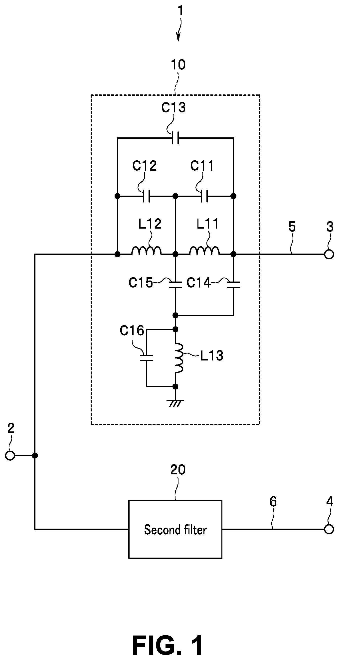
An embodiment of the present invention will now be described in detail with reference to the drawings. First, the configuration of a multilayer electronic component (hereinafter simply referred to as electronic component) 1 according to the embodiment of the invention will be outlined with reference to . shows a branching filter (diplexer) as an example of the electronic component 1 . The branching filter includes a first filter 10 that selectively passes a first signal of a frequency within a first passband, and a second filter 20 that selectively passes a second signal of a frequency within a second passband higher than the first passband.
The electronic component 1 further includes a common port 2 , a first signal port 3 , a second signal port 4 , a first signal path 5 connecting between the common port 2 and the first signal port 3 , a second signal path 6 connecting between the common port 2 and the second port 4 . In the circuit configuration, the first filter 10 is provided between the common port 2 and the first signal port 3 , the second filter 20 is provided between the common port 2 and the second signal port 4 . The first signal path 5 is a path leading from the common port 2 to the first signal port 3 via the first filter 10 . The second signal path 6 is a path leading from the common port 2 to the second signal port 4 via the second filter 20 .
The first signal of a frequency within the first passband selectively passes through the first signal path 5 on which the first filter 10 is provided. The second signal of a frequency within the second passband selectively passes through the second signal path 6 on which the second filter 20 is provided. In such a manner, the electronic component 1 separates the first signal and the second signal.
Next, an example of configuration of the first filter 10 will be described with reference to . The first filter 10 includes inductors L 11 , L 12 , and L 13 , and capacitors C 11 , C 12 , C 13 , C 14 , C 15 , and C 16 . In the circuit configuration, the inductors L 11 and L 12 are provided on the first signal path 5 . In the circuit configuration, the inductor L 11 is provided at a position closer to the first signal port 3 than the inductor L 12 . One end of the inductor L 11 is connected to the first signal port 3 . The other end of the inductor L 11 is connected to one end of the inductor L 12 . The other end of the inductor L 12 is connected to the common port 2 .
The capacitor C 11 is connected in parallel with the inductor L 11 . The capacitor C 12 is connected in parallel with the inductor L 12 . One end of the capacitor C 13 is connected to the one end of the inductor L 11 . The other end of the capacitor C 13 is connected to the other end of the inductor L 12 .
One end of the capacitor C 14 is connected to the one end of the inductor L 11 . One end of the capacitor C 15 is connected to a connection point between the inductor L 11 and the inductor L 12 . The other ends of the capacitors C 14 and C 14 are connected to one end of the inductor L 13 . The other end of the inductor L 13 is connected to the ground. The capacitor C 16 is connected in parallel with the inductor L 13 . In the circuit configuration, the inductor L 13 is provided between the first signal path 5 and the ground.
Next, an example of configuration of the second filter 20 will be described with reference to . The second filter 20 includes inductors L 21 and L 22 , and capacitors C 21 , C 22 , C 23 , C 24 , C 25 , C 26 , C 27 , C 28 , C 29 , C 30 , and C 31 . One end of the capacitor C 21 is connected to the second signal port 4 . The other end of the capacitor C 21 is connected to one end of the capacitor C 22 . The other end of the capacitor C 22 is connected to one end of the capacitor C 23 . The other end of the capacitor C 23 is connected to the common port 2 .
One end of the capacitor C 24 is connected to the one end of the capacitor C 21 . The other end of the capacitor C 24 is connected to the other end of the capacitor C 22 . One end of the capacitor C 25 is connected to a connection point between the capacitor C 22 and the capacitor C 23 .
In the circuit configuration, the inductor L 21 is provided between the second signal path 6 and the ground. The inductor L<includes inductor portions 211 and 212 . One end of the inductor portion 211 is connected to a connection point between the capacitor C 21 and the capacitor C 22 . The other end of the inductor portion 211 is connected to one end of the inductor portion 212 . The other end of the inductor portion 212 is connected to the ground.
In the circuit configuration, the inductor L 22 is provided between the second signal path 6 and the ground. Furthermore, in the circuit configuration, the inductor L 22 is provided at a position closer to the common port 2 than the inductor L 21 . The inductor L 22 includes inductor portions 221 and 222 . One end of the inductor portion 221 is connected to the other end of the capacitor C 25 . The other end of the inductor portion 221 is connected to one end of the inductor portion 222 . The other end of the inductor portion 222 is connected to the ground.
The inductor portion 211 of the inductor L 21 and the inductor portion 221 of the inductor L 22 are magnetically coupled to each other. The inductor portion 212 of the inductor L 21 and the inductor portion 222 of the inductor L 22 are not magnetically coupled to each other.
The capacitor C 26 is connected in parallel with the inductor portion 211 of the inductor L 21 . The capacitor C 27 is connected in parallel with the inductor portion 212 of the inductor L 21 . One end of the capacitor C 28 is connected to the one end of the inductor portion 211 . The other end of the capacitor C 28 is connected to the other end of the inductor portion 212 .
The capacitor C 29 is connected in parallel with the inductor portion 221 of the inductor L 22 . The capacitor C 30 is connected in parallel with the inductor portion 222 of the inductor L 22 . One end of the capacitor C 31 is connected to the one end of the inductor portion 221 . The other end of the capacitor C 31 is connected to the other end of the inductor portion 222 .
Next, other configurations of the electronic component 1 will be described with reference to . is a perspective view showing an appearance of the electronic component 1 .
The electronic component 1 further includes a stack 50 including a plurality of dielectric layers and a plurality of conductors stacked together. The stack 50 is intended to integrate the common port 2 , the first signal port 3 , the second signal port 4 , the inductors L 11 , L 12 , L 13 , L 21 , and L 22 , and the capacitors C 11 to C 16 and C 21 to C 31 . The first filter 10 and the second filter 20 are each constituted by using a plurality of conductors.
The stack 50 has a bottom surface 50 A and a top surface 50 B located at both ends in a stacking direction T of the plurality of dielectric layers, and four side surfaces 50 C to 50 F connecting the bottom surface 50 A and the top surface 50 B. The side surfaces 50 C and 50 D are opposite to each other. The side surfaces 50 E and 50 F are opposite to each other. The side surfaces 50 C to 50 F are perpendicular to the top surface 50 B and the bottom surface 50 A.
Here, X, Y, and Z directions are defined as shown in . The X, Y, and Z directions are orthogonal to one another. In the present embodiment, a direction parallel to the stacking direction T will be referred to as the Z direction. The opposite directions to the X, Y, and Z directions are defined as −X, −Y, and −Z directions, respectively.
As shown in , the bottom surface 50 A is located at the end of the stack 50 in the −Z direction. The top surface 50 B is located at the end of the stack 50 in the Z direction. The bottom surface 50 A and the top surface 50 B each have a rectangular shape extending in the X direction. The side surface 50 C is located at the end of the stack 50 in the −X direction. The side surface 50 D is located at the end of the stack 50 in the X direction. The side surface 50 E is located at the end of the stack 50 in the −Y direction. The side surface 50 F is located at the end of the stack 50 in the Y direction.
A planar shape of the stack 50 , in other words, the shape of the bottom surface 50 A (the shape of the top surface 50 B) in a view in the Z direction is a rectangle. Long sides of the rectangle are parallel to the X direction, and short sides of the rectangle are parallel to the Y direction.
The electronic component 1 further includes signal terminals 112 , 113 , and 114 provided on the bottom surface 50 A of the stack 50 , and ground terminals 111 , 115 , 116 , 117 , 118 , and 119 connected to the ground. The ground terminal 111 is disposed near a corner at a position where the bottom surface 50 A, the side surface 50 D, and the side surface 50 E intersect one another. The signal terminal 113 is disposed near a corner at a position where the bottom surface 50 A, the side surface 50 D, and the side surface 50 F intersect one another. The signal terminal 114 is disposed near a corner at a position where the bottom surface 50 A, the side surface 50 C, and the side surface 50 F intersect one another. The ground terminal 115 is disposed near a corner at a position where the bottom surface 50 A, the side surface 50 C, and the side surface 50 E intersect one another.
The signal terminal 112 is located between the ground terminal 111 and the ground terminal 115 . The ground terminal 116 is located between the ground terminal 111 and the signal terminal 113 . The ground terminal 117 is located between the signal terminal 113 and the signal terminal 114 . The ground terminal 118 is located between the signal terminal 114 and the ground terminal 115 . The ground terminal 119 is disposed at a center of the bottom surface 50 A.
The terminal 112 corresponds to the common port 2 , the signal terminal 113 to the first signal port 3 , and the signal terminal 114 to the second signal port 4 . The common port 2 , the first signal port 3 , and the second signal port 4 are thus provided on the bottom surface 50 A of the stack 50 .
Next, an example of the plurality of dielectric layers and the plurality of conductors constituting the stack 50 will be described with reference to A to B. In this example, the stack 50 includes twenty-four dielectric layers stacked together. The twenty-four dielectric layers will be referred to as a first to a twenty-fourth dielectric layer in the order from bottom to top. The first to twenty-fourth dielectric layers are denoted by reference numerals 51 to 74 , respectively.
In A to C , each circle represents a through hole. The dielectric layers 51 to 72 each have a plurality of through holes. The through holes are each formed by filling a hole intended for a through hole with a conductive paste. Each of the through holes is connected to a conductor layer or another through hole.
A shows the patterned surface of the first dielectric layer 51 . The terminals 111 to 119 are formed on the patterned surface of the dielectric layer 51 . B shows the patterned surface of the second dielectric layer 52 . Conductor layers 521 , 522 , 523 , 524 , and 525 are formed on the patterned surface of the dielectric layer 52 .
C shows the patterned surface of the third dielectric layer 53 . Conductor layers 531 , 532 , 533 , 534 , 535 , 536 , 537 , 538 , 539 , 5310 , 5311 , and 5312 are formed on the patterned surface of the dielectric layer 53 . One end of the conductor layer 531 is connected to the conductor layer 5311 . The other end of the conductor layer 531 is connected to the conductor layer 5312 . In C , the boundary between the conductor layer 531 and the conductor layer 5311 and the boundary between the conductor layer 531 and the conductor layer 5312 are indicated by dotted lines.
A shows the patterned surface of the fourth dielectric layer 54 . Conductor layers 541 , 542 , 543 , 544 , 545 , 546 , 547 , and 548 are formed on the patterned surface of the dielectric layer 54 . The conductor layers 541 and 543 are connected to the conductor layer 542 . B shows the patterned surface of the fifth dielectric layer 55 . Conductor layers 551 , 552 , 553 , and 554 are formed on the patterned surface of the dielectric layer 55 . The conductor layer 554 is connected to the conductor layer 553 . C shows the patterned surface of the sixth dielectric layer 56 . Conductor layers 561 and 562 are formed on the patterned surface of the dielectric layer 56 .
A shows the patterned surface of the seventh dielectric layer 57 . Conductor layers 571 and 572 are formed on the patterned surface of the dielectric layer 57 . The conductor layer 572 is connected to the conductor layer 571 . B shows the patterned surface of the eighth dielectric layer 58 . No conductor layer is formed on the patterned surface of the dielectric layer 58 . C shows the patterned surface of the ninth dielectric layer 59 . A conductor layer 591 is formed on the patterned surface of the dielectric layer 59 .
A shows the patterned surface of the tenth dielectric layer 60 . A conductor layer 601 is formed on the patterned surface of the dielectric layer 60 . B shows the patterned surface of the eleventh dielectric layer 61 . No conductor layer is formed on the patterned surface of the dielectric layer 61 . C shows the patterned surface of the twelfth dielectric layer 62 . Conductor layers 621 and 622 are formed on the patterned surface of the dielectric layer 62 . Shapes of the conductor layers 621 and 622 may be the same in a view in one direction (the Z direction) parallel to the stacking direction T.
A shows the patterned surface of the thirteenth dielectric layer 63 . Conductor layers 631 and 632 are formed on the patterned surface of the dielectric layer 63 . Shapes of the conductor layers 631 and 632 may be the same in a view in one direction (the Z direction) parallel to the stacking direction T. B shows the patterned surface of each of the fourteenth to twenty-first dielectric layers 64 to 71 . No conductor layer is formed on the patterned surface of the dielectric layers 64 to 71 . C shows the patterned surface of the twenty-second dielectric layer 72 . Conductor layers 721 , 722 , 723 , 724 , 725 , 726 , and 727 are formed on the patterned surface of the dielectric layer 72 . Shapes of the conductor layers 722 , 723 , and 724 may be the same in a view in one direction (the Z direction) parallel to the stacking direction T. Shapes of the conductor layers 726 and 727 may be the same in a view in one direction (the Z direction) parallel to the stacking direction T.
A shows the patterned surface of the twenty-third dielectric layer 73 . Conductor layers 731 , 732 , 733 , 734 , 735 , 736 , and 737 are formed on the patterned surface of the dielectric layer 73 . Shapes of the conductor layers 732 , 733 , and 734 may be the same in a view in one direction (the Z direction) parallel to the stacking direction T. Shapes of the conductor layers 736 and 737 may be the same in a view in one direction (the Z direction) parallel to the stacking direction T. B shows the patterned surface of the twenty-fourth dielectric layer 74 . A mark 741 made of a conductor layer is formed on the patterned surface of the dielectric layer 74 .
The stack 50 shown in is formed by stacking the first to twenty-fourth dielectric layers 51 to 74 such that the patterned surface of the first dielectric layer 51 serves as the bottom surface 50 A of the stack 50 and the surface of the twenty-fourth dielectric layer 74 opposite to the patterned surface thereof serves as the top surface 50 B of the stack 50 .
Each of the plurality of through holes shown in A to C is connected to, when the first to twenty-second dielectric layers 51 to 72 are stacked, a conductor layer overlapping in the stacking direction T or to another through hole overlapping in the stacking direction T. Of the plurality of through holes shown in A to C , the ones located within a terminal or a conductor layer are connected to the terminal or conductor layer.
and show an inside of the stack 50 formed by stacking the first to twenty-fourth dielectric layers 51 to 74 . As shown in and , the plurality of conductor layers and the plurality of through holes shown in A to A are stacked together inside the stack 50 . In and , the mark 741 is omitted.
For example, the stack 50 is fabricated by a low-temperature co-firing method, using ceramic as the material of the dielectric layers 51 to 74 . In this case, a plurality of ceramic green sheets, which eventually become the dielectric layers 51 to 74 , are fabricated first. Each ceramic green sheet has a plurality of unfired conductor layers formed thereon and a plurality of unfired through holes formed therein. The plurality of unfired conductor layers eventually become a plurality of conductor layers. The plurality of unfired through holes eventually become a plurality of through holes. Next, the plurality of ceramic green sheets are stacked together into a green sheet stack. The green sheet stack is then cut to form an unfired stack. The ceramic and conductor in the unfired stack are then fired by a low-temperature co-firing method to thereby complete the stack 50 .
Next, configurations of the inductors L 11 , L 12 , L 13 , L 21 , and L 22 will be described in detail with reference to A to . to are side views showing a part of the inside of the stack 50 . shows the part of the inside of the stack 50 in a view from the side surface 50 D side and mainly shows the inductors L 11 , L 12 , and L 13 . shows the part of the inside of the stack 50 in a view from the side surface 50 E side and mainly shows the inductors L 12 , L 13 , and L 22 . shows the part of the inside of the stack 50 in a view from the side surface 50 C side and mainly shows the inductors L 21 and L 22 . shows the part of the inside of the stack 50 in a view from the side surface 50 F side and mainly shows the inductors L 11 and L 21 .
The inductors L 11 , L 12 , L 13 , L 21 , and L 22 are each integrated with the stack 50 . As described later, the inductors L 11 , L 12 , L 21 , and L 22 each include a plurality of through hole columns. The plurality of through hole columns are each constituted by two or more through hole columns arranged in the stacking direction T and connected in series to each other.
First, the configuration of the inductor L 11 will be described. As shown in and , the inductor L 11 is wound about an axis A 11 parallel to a direction orthogonal to the stacking direction T. In the present embodiment, in particular, the axis A 11 extends in a direction parallel to the Y direction.
The inductor L 11 includes one conductor portion wound less than once about the axis A 11 . The conductor portion of the inductor L 11 includes a conductor layer portion 11 C 1 (refer to and ). The conductor layer portion 11 C 1 has a shape that is long in a direction parallel to the X direction. The conductor layer portion 11 C 1 includes conductor layers 721 and 731 (refer to C and A ) disposed at positions different from each other in the stacking direction T and connected in parallel to each other through four through holes. The conductor layers 721 and 731 each extend in the direction parallel to the X direction.
The conductor portion of the inductor L 11 further includes two through hole columns 11 T 1 and two through hole columns 11 T 2 (refer to and ). The two through hole columns 11 T 1 are connected in parallel to a part near one end of the conductor layer portion 11 C 1 in a longitudinal direction. The two through hole columns 11 T 2 are connected in parallel to a part near the other end of the conductor layer portion 11 C 1 in the longitudinal direction.
Next, the configuration of the inductor L 12 will be described. As shown in and , the inductor L 12 is wound about an axis A 12 parallel to a direction orthogonal to the stacking direction T. In the present embodiment, in particular, the axis A 12 extends in a direction parallel to the X direction. The inductor L 12 includes conductor portions L 12 A, L 12 B, and L 12 C each wound less than once about the axis A 12 , a connection portion L 12 D connecting the conductor portions L 12 A and L 12 B in series, and a connection portion L 12 E connecting the conductor portions L 12 B and L 12 C in series.
The conductor portions L 12 A, L 12 B, and L 12 C include conductor layer portions 12 C 1 , 12 C 2 , and 12 C 3 , respectively (refer to and ). The conductor layer portions 12 C 1 , 12 C 2 , and 12 C 3 each have a shape that is long in the direction parallel to the Y direction.
The conductor layer portion 12 C 1 includes conductor layers 722 and 732 (refer to C and A ) disposed at positions different from each other in the stacking direction T and connected in parallel to each other through two through holes. The conductor layer portion 12 C 2 includes conductor layers 723 and 733 (refer to C and A ) disposed at positions different from each other in the stacking direction T and connected in parallel to each other through two through holes. The conductor layer portion 12 C 3 includes conductor layers 724 and 734 (refer to C and A ) disposed at positions different from each other in the stacking direction T and connected in parallel to each other through two through holes. The conductor layers 722 to 724 and 732 to 734 each extend in the direction parallel to the Y direction.
The conductor portion L 12 A further includes through hole columns 12 T 1 and 12 T 2 (refer to and ). The through hole column 12 T 1 is connected to a part near one end of the conductor layer portion 12 C 1 in a longitudinal direction. The through hole column 12 T 2 is connected to a part near the other end of the conductor layer portion 12 C 1 in the longitudinal direction.
The conductor portion L 12 B further includes through hole columns 12 T 3 and 12 T 4 (refer to and ). The through hole column 12 T 3 is connected to a part near one end of the conductor layer portion 12 C 2 in a longitudinal direction. The through hole column 12 T 4 is connected to a part near the other end of the conductor layer portion 12 C 2 in the longitudinal direction.
The conductor portion L 12 C further includes through hole columns 12 T 5 and 12 T 6 (refer to and ). The through hole column 12 T 5 is connected to a part near one end of the conductor layer portion 12 C 3 in a longitudinal direction. The through hole column 12 T 6 is connected to a part near the other end of the conductor layer portion 12 C 3 in the longitudinal direction.
The connection portion L 12 D connects the through hole column 12 T 2 of the conductor portion L 12 A and the through hole column 12 T 3 of the conductor portion L 12 B. The connection portion L 12 D includes a conductor layer portion 12 C 4 (refer to ). The conductor layer portion 12 C 4 includes the conductor layers 621 and 631 (refer to C and A ) disposed at positions different from each other in the stacking direction T and connected in parallel to each other through two through holes.
The connection portion L 12 E connects the through hole column 12 T 4 of the conductor portion L 12 B and the through hole column 12 T 5 of the conductor portion L 12 C. The connection portion L 12 E includes a conductor layer portion 12 C 5 (refer to ). The conductor layer portion 12 C 5 includes the conductor layers 622 and 632 (refer to C and A ) disposed at positions different from each other in the in the stacking direction T and connected in parallel to each other through two through holes.
The conductor layers 542 and 552 shown in A and B are disposed at positions different from each other in the stacking direction T and connected in parallel to each other through three through holes. The conductor layers 542 and 552 connects through hole columns 11 T 3 and 11 T 4 of the conductor portion of the inductor L 11 and the through hole column 12 T 1 of the conductor portion L 12 A of the inductor L 12 .
Next, the configuration of the inductor L 13 will be described. The inductor L 13 is wound about an axis A 13 parallel to the stacking direction T. The inductor L 13 is constituted by the conductor layer 531 (refer to C ).
Next, the configuration of the inductor L 21 will be described. As shown in and , the inductor L 21 is wound about an axis A 21 parallel to a direction orthogonal to the stacking direction T. In the present embodiment, in particular, the axis A 21 extends in a direction parallel to the Y direction.
The inductor L 21 includes one conductor portion wound less than once about the axis A 21 . The conductor portion of the inductor L 21 includes a conductor layer portion 21 C 1 (refer to and ). The conductor layer portion 21 C 1 includes conductor layers 725 and 735 (refer to C and A ) disposed at positions different from each other in the stacking direction T and connected in parallel to each other through two through holes. The conductor layers 725 and 735 each include a first portion extending in the X direction and a second portion extending in the Y direction.
The conductor portion of the inductor L 21 further includes through hole columns 21 T 1 and 21 T 2 (refer to and ). The through hole column 21 T 1 is connected to a part near one end of the conductor layer portion 21 C 1 in a longitudinal direction. The through hole column 21 T 2 is connected to a part near the other end of the conductor layer portion 21 C 1 in the longitudinal direction.
The inductor L 21 further includes conductor layer portions 21 C 2 and 21 C 3 (refer to ). The conductor layer portion 21 C 1 connects one end of the through hole column 21 T 1 and one end of the through hole column 21 T 2 . The conductor layer portion 21 C 2 is connected to the other end of the through hole column 21 T 1 and extends close to the other end of the through hole column 21 T 2 . The conductor layer portion 21 C 3 is connected to the other end of the through hole column 21 T 2 and extends close to the other end of the through hole column 21 T 1 .
The conductor layer portion 21 C 2 includes conductor layers 561 and 571 (refer to C and A ) disposed at positions different from each other in the stacking direction T and connected in parallel to each other through two through holes. The conductor layer portion 21 C 3 includes conductor layers 544 and 553 (refer to A and B ) disposed at positions different from each other in the stacking direction T and connected in parallel to each other through two through holes.
The conductor layer portions 21 C 1 and 21 C 2 and the through hole columns 21 T 1 and 21 T 2 constitute the inductor portion 211 of the inductor L 21 . The conductor layer portion 21 C 3 constitutes the inductor portion 212 of the inductor L 21 . The conductor layer portion 21 C 3 (conductor layers 544 and 553 ) is connected to the ground terminal 117 through the conductor layers 526 and 5310 (refer to B and C ) and a plurality of through holes.
Next, the configuration of the inductor L 22 will be described. As shown in and , the inductor L 22 is wound about an axis A 22 parallel to a direction orthogonal to the stacking direction T. In the present embodiment, in particular, the axis A 22 extends in a direction parallel to the Y direction. The inductor L 22 includes conductor portions L 22 A and L 22 B each wound less than once about the axis A 22 , and a connection portion L 22 C connecting the conductor portions L 22 A and L 22 B in series.
The conductor portions L 22 A and L 22 B include conductor layer portions 22 C 1 and 22 C 2 , respectively (refer to and ). The conductor layer portions 22 C 1 and 22 C 2 each have a shape that is long in the direction parallel to the X direction.
The conductor layer portion 22 C 1 includes conductor layers 726 and 736 (refer to C and A ) disposed at positions different from each other in the stacking direction T and connected in parallel to each other through four through holes. The conductor layer portion 22 C 2 includes conductor layers 727 and 737 (refer to C and A ) disposed at positions different from each other in the stacking direction T and connected in parallel to each other through four through holes. The conductor layers 726 , 727 , 736 and 737 each extend in the direction parallel to the X direction.
The conductor portion L 22 A further includes two through hole columns 22 T 1 and two through hole columns 22 T 2 (refer to and ). The two through hole columns 22 T 1 are connected in parallel to a part near one end of the conductor layer portion 22 C 1 in a longitudinal direction. The two through hole columns 22 T 2 are connected in parallel to a part near the other end of the conductor layer portion 22 C 1 in the longitudinal direction.
The conductor portion L 22 B further includes two through hole columns 22 T 3 and two through hole columns 22 T 4 (refer to and ). The two through hole columns 22 T 3 are connected in parallel to a part near one end of the conductor layer portion 22 C 2 in a longitudinal direction. The two through hole columns 22 T 4 are connected in parallel to a part near the other end of the conductor layer portion 22 C 2 in the longitudinal direction.
The connection portion L 22 C connects the two through hole columns 22 T 2 of the conductor portion L 22 A and the two through hole columns 22 T 3 of the conductor portion L 22 B. The connection portion L 22 C includes a conductor layer portion 22 C 3 (refer to and ). The conductor layer portion 22 C 3 includes the conductor layers 591 and 601 (refer to C and A ) disposed at positions different from each other in the in the stacking direction T and connected in parallel to each other through four through holes.
The conductor layer portion L 22 A constitutes the inductor portion 221 of the inductor L 22 . The conductor layer portion L 22 B constitutes the inductor portion 222 of the inductor L 22 . In the circuit configuration, the conductor portion L 22 B is provided between the conductor portion L 22 A and the ground. The two through hole columns 22 T 4 of the conductor portion L 22 B are connected to the ground terminals 115 and 118 through the conductor layers 525 and 539 (refer to B and C ) and a plurality of through holes.
Correspondences between the capacitors C 11 to C 16 and C 21 to C 31 and the internal components of the stack 50 shown in A to B will now be described. The capacitor C 11 is composed of the conductor layers 521 , 532 , 541 , and 551 shown in B to A , C , and A , and the dielectric layers 52 , 53 , and 54 each interposed between two of those conductor layers. The capacitor C 12 is composed of the conductor layers 621 , 622 , 631 , 632 , 722 to 724 , and 732 to 734 shown in C , A , C , and A , and the dielectric layers 62 and 72 each interposed between two of those conductor layers. The capacitor C 13 is composed of the conductor layers 721 to 724 and 731 to 734 .
The capacitor C 14 is composed of the conductor layers 5311 and 532 shown in C . The capacitor C 15 is composed of the conductor layer 5311 , the conductor layer 542 shown in A , and the dielectric layer 53 interposed between two of those conductor layers. The capacitor C 16 is composed of the conductor layers 5312 and 543 shown in C and A , and the dielectric layer 53 interposed between two of those conductor layers.
The capacitor C 21 is composed of the conductor layers 533 and 545 shown in C and A , and the dielectric layer 53 interposed between those conductor layers. The capacitor C 22 is composed of the conductor layers 534 and 545 shown in C , A , and C , and the dielectric layer 53 interposed between those conductor layers. The capacitor C 23 is composed of the conductor layers 535 and 546 shown in C and A , and the dielectric layer 53 interposed between those conductor layers. The capacitor C 24 is composed of the conductor layers 533 and 534 . The capacitor C 25 is composed of the conductor layers 536 , 546 , and 547 shown in C , A , and C , and the dielectric layer 53 interposed between two of those conductor layers.
The capacitor C 26 is composed of the conductor layers 561 , 571 , 725 , and 735 shown in C , A , C , and A , and the dielectric layers 56 and 72 interposed between two of those conductor layers. The capacitor C 27 is composed of the conductor layers 544 and 553 shown in A and B , and the dielectric layer 54 interposed between those conductor layers. The capacitor C 28 is composed of the conductor layers 554 and 572 shown in B and A , and the dielectric layers 55 and 56 each interposed between those conductor layers.
The capacitor C 29 is composed of the conductor layers 591 , 601 , 726 , and 736 shown in C , A , C , and A , and the dielectric layers 59 and 72 each interposed between two of those conductor layers. The capacitor C 30 is composed of the conductor layers 591 and 601 , and the conductor layers 727 and 737 shown in C and A , and the dielectric layers 59 and 72 each interposed between those conductor layers. The capacitor C 31 is composed of the conductor layers 537 and 548 shown in C and A , and the dielectric layer 53 interposed between those conductor layers.
Next, structural features of the electronic component 1 according to the present embodiment will be described with reference to to . and are plan views showing a part of an inside of the stack 50 shown in and .
As shown in to , the inductor L 12 is disposed after the inductor L 11 in one direction orthogonal to the stacking direction T, in other words, the −Y direction. The inductor L 21 and the inductor L 22 are disposed after the inductor L 11 and the inductor L 12 , respectively, in one direction orthogonal to the stacking direction T, in other words, the −X direction.
In and , a region surrounded by a dashed line denoted by a reference numeral S 11 shows a space including the axis A 11 and surrounded by the inductor L 11 . In and , a region surrounded by a dashed line denoted by a reference numeral S 12 shows a space including the axis A 12 and surrounded by the inductor L 12 . In and , a region surrounded by a dashed line denoted by a reference numeral S 21 shows a space including the axis A 21 and surrounded by the inductor L 21 . In and , a region surrounded by a dashed line denoted by a reference numeral S 22 shows a space including the axis A 22 and surrounded by the inductor L 22 .
In , the region surrounded by a dashed line denoted by the reference numeral S 11 is also a region obtained by vertically projecting the space S 11 onto a virtual plane (XZ plane) perpendicular to the axis A 11 . Hereinafter, the region is referred to as a projection region of the space S 11 . Area of the projection region of the space S 11 corresponds to opening area of the inductor L 11 .
In , the region surrounded by a dashed line denoted by the reference numeral S 12 is also a region obtained by vertically projecting the space S 12 onto a virtual plane (YZ plane) perpendicular to the axis A 12 . Hereinafter, the region is referred to as a projection region of the space S 12 . Area of the projection region of the space S 12 corresponds to opening area of the inductor L 12 .
In , the region surrounded by a dashed line denoted by the reference numeral S 21 is also a region obtained by vertically projecting the space S 21 onto a virtual plane (XZ plane) perpendicular to the axis A 21 . Hereinafter, the region is referred to as a projection region of the space S 21 . Area of the projection region of the space S 21 corresponds to opening area of the inductor L 21 .
In , the region surrounded by a dashed line denoted by the reference numeral S 22 is also a region obtained by vertically projecting the space S 22 onto a virtual plane (XZ plane) perpendicular to the axis A 22 . Hereinafter, the region is referred to as a projection region of the space S 22 . Area of the projection region of the space S 22 corresponds to opening area of the inductor L 22 .
As shown in and , the area of the projection region of the space S 11 is larger than the area of the projection region of the space S 12 . As shown in and , the area of the projection region of the space S 21 is larger than the area of the projection region of the space S 12 . As shown in and , the area of the projection region of the space S 22 is larger than the area of the projection region of the space S 12 .
As shown in and , the area of the projection region of the space S 21 and the area of the projection region of the space S 22 are different from each other. In the present embodiment, in particular, the area of the projection region of the space S 21 is larger than the area of the projection region of the space S 22 . A dimension of the projection region of the space S 21 in the stacking direction T is larger than a dimension of the projection region of the space S 22 in the stacking direction T.
The inductor L 11 is disposed such that part of the space S 11 overlaps at least part of the space S 12 in a view in one direction (the Y direction) parallel to the axis A 11 .
The inductor L 12 is disposed such that at least part of the space S 12 overlaps the space S 22 in a view in one direction (the X direction) parallel to the axis A 12 . The inductor L 12 is disposed such that the axis A 12 is parallel to the long sides of the bottom surface 50 A of the stack 50 (the long sides of the top surface 50 B).
The inductor L 13 is disposed such that the axis A 13 does not intersect the spaces S 11 , S 21 , and S 22 but intersects the space S 12 . In other words, the inductor L 13 is disposed such that the inductor L 13 overlaps the inductor L 12 in a view in the Z direction. No capacitor conductor layer used to constitute a capacitor is interposed between the inductor L 12 and the inductor L 13 , more specifically, between the conductor layer 531 (refer to C ) and the conductor layers 621 and 622 (refer to C ).
The inductor L 21 is disposed such that at least part of the space S 21 overlaps at least part of the space S 22 in a view in one direction (the Y direction) parallel to the axis A 21 . In other words, the inductor L 22 is disposed such that at least part of the space S 22 overlaps part of the space S 21 in a view in one direction (the Y direction) parallel to the axis A 22 .
The conductor layer portion 21 C 3 of the inductor L 21 is disposed between the conductor layer portion 21 C 1 of the inductor L 21 and the bottom surface 50 A. The conductor layer portion 21 C 3 extends across the signal terminal 114 in a view in one direction (the Z direction) parallel to the stacking direction T. The inductor L 21 is electrically connected to the ground terminal 117 . The inductor L 22 is electrically connected to the ground terminals 115 and 118 .
The inductor L 22 includes the conductor portion L 22 A constituting the inductor portion 221 of the inductor L 22 , the conductor portion L 22 B constituting the inductor portion 222 of the inductor L 22 , and the connection portion L 22 C connecting the conductor portions L 22 A and L 22 B in series. The conductor portion L 22 A (inductor portion 221 ) is magnetically coupled to the conductor layer portions 21 C 1 and 21 C 2 constituting the inductor portion 211 of the inductor L 21 , and the through hole columns 21 T 1 and 21 T 2 in the inductor L 21 .
shows the two conductor layers 721 and 731 constituting the conductor layer portion 11 C 1 of the inductor L 11 . As shown in , area of the conductor layer 721 is larger than area of the conductor layer 731 . The conductor layer 731 is disposed inside an outer edge of the conductor layer 721 in a view in one direction (the Z direction) parallel to the stacking direction T. A shape of the conductor layer 731 in a view in the Z direction is similar to a shape of the conductor layer 721 in a view in the Z direction. The conductor layer 721 is disposed between the conductor layer 731 and the axis A 11 .
The above description on the conductor layers 721 and 731 also applies to pairs of the conductor layers 72 x and 73 x (x is an integer of two to seven). Description on the conductor layers 72 x and 73 x is obtained by replacing the conductor layers 721 and 731 in the above description on the conductor layers 721 and 731 with the conductor layers 72 x and 73 x , respectively. In a case of description on pairs of the conductor layers 72 x and 73 x constituting the inductor L 12 , the axis A 11 in the above description is replaced with the axis A 12 . In a case of description on pairs of the conductor layers 725 and 735 constituting the inductor L 21 , the axis A 11 in the above description is replaced with the axis A 21 . In a case of description on pairs of the conductor layers 72 x and 73 x constituting the inductor L 22 , the axis A 11 in the above description is replaced with the axis A 22 .
shows the two conductor layers 621 and 631 constituting the conductor layer portion 12 C 4 of the inductor L 12 . As shown in , area of the conductor layer 631 is larger than area of the conductor layer 621 . The conductor layer 621 is disposed inside an outer edge of the conductor layer 631 in a view in one direction (the Z direction) parallel to the stacking direction T. A shape of the conductor layer 621 in a view in the Z direction is similar to a shape of the conductor layer 631 in a view in the Z direction. The conductor layer 631 is disposed between the conductor layer 621 and the axis A 12 .
The above description on the conductor layers 621 and 631 also applies to the pair of the conductor layers 622 and 632 , the pair of the conductor layers 561 and 571 , the pair of the conductor layers 543 and 553 , and the pair of the conductor layers 591 and 601 . Description on the conductor layers 622 and 632 is obtained by replacing the conductor layers 621 and 631 in the above description on the conductor layers 621 and 631 with the conductor layers 622 and 632 , respectively.
Description on the conductor layers 561 and 571 or the conductor layers 543 and 553 is obtained by replacing the conductor layers 621 and 631 in the above description on the conductor layers 621 and 631 with the conductor layers 561 and 571 or the conductor layers 543 and 553 , respectively, and replacing the axis A 12 in the above description on the conductor layers 621 and 631 with the axis A 21 .
Description on the conductor layers 591 and 601 is obtained by replacing the conductor layers 621 and 631 in the above description on the conductor layers 621 and 631 with the conductor layers 591 and 601 , respectively, and replacing the axis A 12 in the above description on the conductor layers 621 and 631 with the axis A 22 .
Next, an example of the characteristics of the electronic component 1 according to the present embodiment will be described. is a characteristic diagram showing a pass characteristic between the common port 2 and the first signal port 3 , in other words, a pass characteristic of the first filter 10 . is a characteristic diagram showing a pass characteristic between the common port 2 and the second signal port 4 , in other words, a pass characteristic of the second filter 20 . In and , the horizontal axis indicates frequency, and the vertical axis the attenuation.
In , a reference numeral 91 denotes an attenuation pole formed by the inductor L 11 , and a reference numeral 92 denotes an attenuation pole formed by the inductor L 12 . The inductor L 12 forms the attenuation pole 92 on a high-pass side of the first passband in the pass characteristic of the first filter 10 . The inductor L 11 forms the attenuation pole 91 between the first passband and the attenuation pole 92 in the pass characteristic of the first filter 10 . In other words, in the pass characteristic of the first filter 10 , the attenuation pole 91 formed by the inductor L 11 is closer to the first passband than the attenuation pole 92 formed by the inductor L 12 .
In , a reference numeral 93 denotes an attenuation pole formed by the inductor L 21 , and a reference numeral 94 denotes an attenuation pole formed by the inductor L 22 . The inductor L 21 forms the attenuation pole 93 on a low-pass side of the second passband in the pass characteristic of the second filter 20 . The inductor L 22 forms the attenuation pole 94 between the attenuation pole 93 and the second passband in the pass characteristic of the second filter 20 . In other words, in the pass characteristic of the second filter 20 , the attenuation pole 94 formed by the inductor L 22 is closer to the second passband than the attenuation pole 93 formed by the inductor L 21 .
Next, an example of inductance and a Q value of each of the inductors L 11 , L 12 , L 13 , L 21 , and L 22 will be described. In the example, the inductance of the inductor L 11 is 0.8 nH. The Q value of the inductor L 11 is 125. The inductance of the inductor L 12 is 3.4 nH. The Q value of the inductor L 12 is 113. The inductance of the inductor L 13 is 0.81 nH. The Q value of the inductor L 13 is 53. The inductance of the inductor L 21 is 1.5 nH. The Q value of the inductor L 21 is 73. The inductance of the inductor L 22 is 2.0 nH. The Q value of the inductor L 22 is 127.
Now, the operation and effects of the electronic component 1 according to the present embodiment will be described. In the present embodiment, the conductor layer portion 21 C 1 of the inductor L 21 includes the two conductor layers 725 and 735 . As described above, in a manufacturing process of the stack 50 , ceramic green sheets on which a plurality of unfired conductor layers and a plurality of unfired through holes are formed are stacked, the plurality of unfired conductor layers eventually becoming a plurality of conductor layers, the plurality of unfired through holes eventually becoming a plurality of through holes. A characteristic of the inductor L 21 changes when the conductor layer 725 and the conductor layer 735 are displaced from each other due to displacement of the ceramic green sheets, the plurality of unfired conductor layers, or the like.
However, in the present embodiment, area of the conductor layer 725 is larger than area of the conductor layer 735 . Thus, even if the conductor layer 735 is relatively displaced from the conductor layer 725 , the conductor layer 735 entirely or mostly does not extend out of the conductor layer 725 in a view in one direction (the Z direction) parallel to the stacking direction T. Thus, according to the present embodiment, it is possible to reduce characteristic variation of the inductor L 21 due to displacement of the conductor layer 725 and the conductor layer 735 from each other.
The above description on the conductor layers 725 and 735 also applies to pairs of the conductor layers 72 x and 73 x (x is an integer of one to four or an integer of six or seven), the pair of the conductor layers 621 and 631 , the pair of the conductor layers 622 and 632 , the pair of the conductor layers 561 and 571 , the pair of the conductor layers 543 and 553 , and the pair of the conductor layers 591 and 601 . Thus, according to the present embodiment, it is possible to reduce characteristic variation of each of the first filter 10 and the second filter 20 due to displacement of the ceramic green sheets, the plurality of unfired conductor layers, or the like, and as a result, it is possible to reduce characteristic variation of the electronic component 1 .
A shape of a conductor layer in a view in one direction (the Z direction) parallel to the stacking direction T is referred to as a planar shape of the conductor layer. In a view in one direction (the Z direction) parallel to the stacking direction T, a conductor layer having the larger area among the two conductor layers constituting each conductor layer portion may have a planar shape extending by 5 to 500 μm out of a conductor layer having the smaller area in every direction (direction parallel to an XY plane).
Next, the effects of the present embodiment will be described with reference to results of first to third simulations. First, the result of the first simulation on variation in the inductance of the inductor L 21 will be described. In the first simulation, a model of the inductor L 21 in the present embodiment and a model of an inductor of a first comparative example were used. Configuration of the inductor of the first comparative example is the same as the configuration of the inductor L 21 except for the conductor layer portion 21 C 1 . The inductor of the first comparative example includes a conductor layer portion of a comparative example in place of the conductor layer portion 21 C 1 . The conductor layer portion of the comparative example includes a first conductor layer and a second conductor layer disposed at positions different from each other in the stacking direction T and connected in parallel to each other through two through holes. The second conductor layer is positioned after the first conductor layer in the Z direction.
In the first simulation, a planar shape of each of the first and second conductor layers is the same as a planar shape of the conductor layer 735 in the present embodiment. Specifically, conductor layers having the same planar shape are stacked at the conductor layer portion of the comparative example.
In the first simulation, the inductor L 21 was designed such that the inductance of the inductor L 21 is 1.452 nH, and the inductor of the first comparative example was designed such that inductance of the inductor of the first comparative example is 1.444 nH. A dimension of the planar shape of a conductor layer in a direction orthogonal to a longitudinal direction of the conductor layer is referred to as a width of the conductor layer. In the first simulation, a width of the conductor layer 725 of the inductor L 21 was 225 μm, and a width of the conductor layer 735 of the inductor L 21 was 175 μm. A width of each of the first and second conductor layers was 225 μm.
The first simulation calculated the inductance of the inductor L 21 when the conductor layer 735 was displaced by 15 μm in each of the X direction, the −X direction, the Y direction, and the −Y direction. The first simulation also calculated the inductance of the inductor of the first comparative example when the second conductor layer was displaced by 15 μm in each of the X direction, the −X direction, the Y direction, and the −Y direction.
Table 1 and Table 2 show the result of the first simulation. Table 1 shows inductance values (in the unit of nH) obtained by the first simulation. Table 2 shows a change amount of inductance from a designed value when the conductor layer 735 and the second conductor layer were each displaced in the X direction, the −X direction, the Y direction, and the −Y direction. In the first simulation and the second simulation to be described later, the change amount is a value as a percentage expression of a value obtained by dividing, by inductance of a designed value, a difference between inductance obtained by the simulation and the inductance of the designed value. In Table 1 and Table 2, “First comparative example” and “L 21 ” mean the model of the inductor of the first comparative example and the model of the inductor L 21 , respectively. In Table 1 and Table 2, “X direction”, “−X direction”, “Y direction”, and “−Y direction” mean directions in which the conductor layer 735 or the second conductor layer was displaced.
TABLE 1
Designed X −X Y −Y
value direction direction direction direction
First 1.444 1.452 1.462 1.442 1.454
comparative
example
L21 1.452 1.450 1.453 1.448 1.452
TABLE 2
X −X Y −Y
direction direction direction direction
First 0.5% 1.2% −0.1% 0.7%
comparative
example
L21 −0.1% 0.1% −0.2% 0.0%
It is understood from Table 2 that an absolute value of the change amount of the inductance of the inductor L 21 is smaller than an absolute value of the change amount of the inductance of the inductor of the first comparative example.
Next, the result of the second simulation on variation in the inductance of the inductor L 12 will be described. In the second simulation, a model of the inductor L 12 in the present embodiment and a model of an inductor of a second comparative example were used. Configuration of the inductor of the second comparative example is the same as the configuration of the inductor L 12 except for the conductor layer portions 12 C 1 , 12 C 2 , and 12 C 3 . The inductor of the second comparative example includes three conductor layer portions of the comparative example described above in place of the conductor layer portions 12 C 1 to 12 C 3 . In the second simulation, shapes of first and second conductor layers of the conductor layer portion of the comparative example are the same as a planar shape of the conductor layer 732 in the present embodiment.
In the second simulation, the inductor L 12 was designed such that the inductance of the inductor L 12 is 3.289 nH, and the inductor of the second comparative example was designed such that inductance of the inductor of the second comparative example is 3.274 nH. In the second simulation, a width of each of the conductor layers 722 , 723 , and 724 of the inductor L 12 was 246 μm, and a width of each of the conductor layers 732 , 733 , and 734 of the inductor L 12 was 196 μm. A width of each of the first and second conductor layers was 246 μm.
The second simulation calculated the inductance of the inductor L 12 when each of the conductor layers 722 , 723 , and 724 was displaced by 15 μm in each of the X direction, the −X direction, the Y direction, and the −Y direction. The second simulation also calculated the inductance of the inductor of the second comparative example when the second conductor layer of each of the three conductor layer portions was displaced by 15 μm in each of the X direction, the −X direction, the Y direction, and the −Y direction.
Table 3 and Table 4 show the result of the second simulation. Table 3 shows inductance values (in the unit of nH) obtained by the second simulation. Table 4 shows a change amount of inductance from a designed value when the conductor layers 722 , 723 , and 724 and the second conductor layer were each displaced in the X direction, the −X direction, the Y direction, and the −Y direction. In Table 3 and Table 4, “Second comparative example” and “L 12 ” mean the model of the inductor of the second comparative example and the model of the inductor L 12 , respectively.
TABLE 3
Designed X −X Y −Y
value direction direction direction direction
Second 3.274 3.283 3.272 3.285 3.282
comparative
example
L12 3.289 3.289 3.282 3.296 3.288
TABLE 4
X −X Y −Y
direction direction direction direction
Second 0.3% −0.1% 0.3% 0.2%
comparative
example
L12 −0.0% −0.2% 0.2% −0.1%
It is understood from Table 4 that an absolute value of the change amount of the inductance of the inductor L 12 is smaller than an absolute value of the change amount of the inductance of the inductor of the second comparative example.
As understood from the results of the first and second simulations, according to the present embodiment, it is possible to reduce inductor characteristic variation due to conductor layer displacement as compared to an inductor including a conductor layer portion at which conductor layers having the same planar shape are stacked.
It is understood from Table 2 and Table 4 that the change amount of the inductance of the inductor of the first comparative example is larger than the change amount of the inductance of the inductor of the second comparative example. Specifically, the inductance change amount when conductor layers are displaced is larger for an inductor, such as the inductor of the first comparative example or the inductor L 21 , including a conductor layer portion having an L-shaped planar shape than for an inductor, such as the inductor of the first comparative example or the inductor L 12 , including a conductor layer portion having a straight planar shape. This is thought to be because, in a conductor layer portion having an L-shaped planar shape, a shortest path between two through hole columns connected to each other through the conductor layer portion largely changes with conductor layer displacement. Thus, the effects of the present embodiment are more significantly exerted for an inductor including a conductor layer portion having an L-shaped planar shape.
The above description on an inductor including a conductor layer portion having an L-shaped planar shape also applies to an inductor including a conductor layer portion having a U-shaped planar shape and to an inductor including a conductor layer portion having a spiral planar shape.
Next, the result of the third simulation on characteristic variation of the electronic component 1 will be described. In the third simulation, a model of a practical example corresponding to the electronic component 1 according to the present embodiment and a model of an electronic component of a comparative example were used. Configuration of the electronic component of the comparative example is the same as configuration of the electronic component 1 except for conductor layer portions included in the inductors L 11 , L 12 , L 21 , and L 22 . The electronic component of the comparative example includes the above-described conductor layer portion of the comparative example as each conductor layer portion. The planar shape of each of the first and second conductor layers included in each conductor layer portion is the same as the planar shape of a conductor layer having the smaller area among the two conductor layers included in a conductor layer portion in the present embodiment corresponding to the conductor layer portion.
The third simulation calculated variation in frequency characteristics of the first filter 10 and the second filter 20 when a dielectric layer 23 was displaced by 15 μm in each of the X direction, the −X direction, the Y direction, and the −Y direction. A frequency at which attenuation is −10 dB when the frequency is increased from the first passband in the frequency characteristic of the first filter 10 is referred to as a first frequency. A frequency at which attenuation is −10 dB when the frequency is decreased from the second passband in the frequency characteristic of the second filter 20 is referred to as a second frequency. The third simulation calculated a change amount of the first frequency as variation in the frequency characteristic of the first filter 10 . Specifically, a reference frequency was set to be the first frequency when a displacement amount of the dielectric layer 23 was 0 μm, and an absolute value of a value as a percentage expression of a value, obtained by dividing by the reference frequency a difference between the first frequency obtained by the third simulation and the reference frequency, was calculated as the change amount of the first frequency. As in the change amount of the first frequency, the third simulation also calculated a change amount of the second frequency as variation in the frequency characteristic of the second filter 20 .
Table 5 and Table 6 show the result of the third simulation. Table 5 shows the change amount of the first frequency obtained by the third simulation. Table 6 shows the change amount of the second frequency obtained by the third simulation. In Table 5 and Table 6, “Comparative example” and “Practical example” mean the model of the electronic component of the comparative example and the model of the practical example, respectively. In Table 5 and Table 6, “X direction”, “−X direction”, “Y direction”, and “−Y direction” mean directions in which the dielectric layer 23 was displaced.
TABLE 5
X −X Y −Y Average
direction direction direction direction value
Comparative 0.021% 0.058% 0.004% 0.004% 0.022%
example
Practical 0.028% 0.009% 0.002% 0.002% 0.011%
example
TABLE 6
X −X Y −Y Average
direction direction direction direction value
Comparative 0.032% 0.087% 0.045% 0.042% 0.051%
example
Practical 0.044% 0.016% 0.014% 0.005% 0.020%
example
It is understood from Table 5 and Table 6 that the change amount of the first frequency and the change amount of the second frequency are smaller for the electronic component 1 according to the present embodiment than for the electronic component of the comparative example. As understood from the result of the third simulation, according to the present embodiment, it is possible to reduce characteristic variation of the first filter 10 and the second filter 20 , and as a result, it is possible to reduce characteristic variation of the electronic component 1 .
Next, other effects of the present embodiment will be described. In the present embodiment, the area of the projection region of the space S 11 corresponding to the opening area of the inductor L 11 is larger than the area of the projection region of the space S 12 corresponding to the opening area of the inductor L 12 . In other words, in the present embodiment, the area of the projection region of the space S 12 corresponding to the opening area of the inductor L 12 is smaller than the area of the projection region of the space S 11 corresponding to the opening area of the inductor L 11 . Accordingly, a space for disposing another inductor can be formed near the inductor L 12 . In the present embodiment, the inductor L 13 is disposed in the above-described space. As described above, the inductor L 13 is disposed such that the axis A 13 does not intersect the space S 11 but intersects the space S 12 . In the present embodiment, the inductors L 11 , L 12 , and L 13 are wound about respective axes parallel to directions different from one another. In the present embodiment, in particular, the axes A 11 , A 12 , and A 13 are orthogonal to one another. Thus, according to the present embodiment, it is possible to prevent electromagnetic coupling among the inductors L 11 , L 12 , and L 13 and also downsize the electronic component 1 .
In the present embodiment, the inductor L 11 is disposed such that part of the space S 11 overlaps at least part of the space S 12 in a view in one direction parallel to the axis A 11 . Thus, according to the present embodiment, it is possible to downsize the electronic component 1 as compared to configuration in which the space S 11 and the space S 12 do not overlap each other.
According to the present embodiment, the first filter 10 includes the inductors L 11 , L 12 , and L 13 . According to the present embodiment, it is possible to reduce a region of the first filter 10 in the stack 50 because of the above-described characteristics of the inductors L 11 , L 12 , and L 13 , and as a result, it is possible to downsize the electronic component 1 .
In the present embodiment, the area of the projection region of the space S 12 corresponding to the opening area of the inductor L 12 is smaller than the area of the projection region of the space S 22 corresponding to the opening area of the inductor L 22 . In the present embodiment, the inductors L 12 , L 13 , and L 22 are wound about respective axes parallel to directions different from one another. In the present embodiment, in particular, the axes A 12 , A 13 , and A 22 are orthogonal to one another. Thus, according to the present embodiment, it is possible to prevent electromagnetic coupling among the inductors L 12 , L 13 , and L 22 and also downsize the electronic component 1 .
In the present embodiment, the inductor L 12 is disposed such that part of the space S 12 overlaps at least part of the space S 22 in a view in one direction parallel to the axis A 12 . Thus, according to the present embodiment, it is possible to downsize the electronic component 1 as compared to configuration in which the space S 12 and the space S 22 do not overlap each other.
In the present embodiment, no capacitor conductor layer is interposed between the inductor L 12 and the inductor L 13 . Thus, according to the present embodiment, it is possible to downsize the electronic component 1 as compared to configuration in which a capacitor conductor layer is interposed between the inductor L 12 and the inductor L 13 .
In the present embodiment, the first filter 10 includes the inductors L 12 and L 13 , and the second filter 20 includes the inductor L 22 . According to the present embodiment, it is possible to place the first filter 10 and the second filter 20 close to each other because of the above-described characteristics of the inductors L 12 , L 13 , and L 22 , and as a result, it is possible to downsize the electronic component 1 .
Since the area of the projection region of the space S 12 corresponding to the opening area of the inductor L 12 is small, the inductance of the inductor L 12 is relatively small. However, in the present embodiment, the inductor L 12 includes the conductor portions L 12 A, L 12 B, and L 12 C each wound less than once about the axis A 12 . In other words, in the present embodiment, the inductor L 12 is wound approximately three times about the axis A 12 . Thus, according to the present embodiment, it is possible to increase the inductance of the inductor L 12 . Moreover, according to the present embodiment, it is possible to increase a dimension of the inductor L 12 in a direction parallel to the axis A 12 (the direction parallel to the X direction). Thus, according to the present embodiment, it is possible to increase the space for disposing the inductor L 13 .
In the present embodiment, the inductor L 12 is disposed such that the axis A 12 is parallel to the long sides of the bottom surface 50 A of the stack 50 (the long sides of the top surface 50 B). Thus, according to the present embodiment, it is possible to dispose another inductor, specifically the inductor L 22 , in a direction parallel to the axis A 12 and also wind the inductor L 12 a plurality of times about the axis A 12 .
In the present embodiment, the inductors L 11 and L 12 are provided on the first signal path 5 in the circuit configuration, and the inductor L 13 is provided between the first signal path 5 and the ground in the circuit configuration. The Q value of the inductor L 13 may be smaller than the Q values of the inductors L 11 and L 12 . As described above, in the example, the Q value of the inductor L 11 is 125, the Q value of the inductor L 12 is 113, and the Q value of the inductor L 13 is 53. In the present embodiment, the inductors L 11 and L 12 , which preferably have relatively large Q values, are inductors wound about an axis orthogonal to the stacking direction T, and the inductor L 13 , which may have a relatively small Q value, is an inductor wound about an axis parallel to the stacking direction T. The inductor L 13 , which may have a relatively small Q value, is disposed in the space formed near the inductor L 12 .
In the present embodiment, the inductor L 21 is disposed such that part of the space S 21 overlaps at least part of the space S 22 in a view in one direction (the Y direction) parallel to the axis A 21 . In other words, the inductor L 22 is disposed such that at least part of the space S 22 overlaps part of the space S 22 in a view in one direction (the Y direction) parallel to the axis A 22 . In the present embodiment, in particular, the axis A 21 and the axis A 22 are parallel to each other. Thus, in the present embodiment, the inductors L 21 and L 22 are disposed such that an opening of the inductor L 21 and an opening of the inductor L 22 face each other and the inductor L 21 and the inductor L 22 overlap each other in a view in the Y direction.
Consider a case in which magnetic coupling between the inductor L 21 and the inductor L 22 is adjusted. For example, the magnetic coupling can be adjusted by displacing one of the inductors L 21 and L 22 in the X direction or the −X direction. With this configuration, an unnecessary space is generated in the stack 50 , and a planar shape of the electronic component 1 (shape in a view in the Z direction) becomes large.
However, in the present embodiment, the area of the projection region of the space S 21 and the area of the projection region of the space S 22 are different from each other. Thus, according to the present embodiment, it is possible to adjust the magnetic coupling without displacing one of the inductors L 21 and L 22 in the X direction or the −X direction.
Consider a case in which a dimension of the inductor L 21 in the stacking direction T is increased to adjust the area of the projection region of the space S 21 . In this case, a distance from the bottom surface 50 A of the stack 50 to the inductor L 21 is shortened. When a ground terminal is provided near the inductor L 21 , floating capacitance is generated between the inductor L 21 and the ground terminal and a desired characteristic is potentially not obtained.
However, in the present embodiment, the inductor L 21 includes the conductor layer portion 21 C 2 connected to the other end of the through hole column 21 T 1 and extending close to the other end of the through hole column 21 T 2 , and the conductor layer portion 21 C 3 connected to the other end of the through hole column 21 T 2 and extending close to the other end of the through hole column 21 T 1 . According to the present embodiment, with at least one of the conductor layer portions 21 C 2 and 21 C 3 , the inductor L 21 can be disposed such that the inductor L 21 does not overlap the ground terminal in a view in one direction (the Z direction) parallel to the stacking direction T. In the present embodiment, in particular, the conductor layer portion 21 C 3 extends across the signal terminal 114 in a view in one direction (the Z direction) parallel to the stacking direction T. Thus, according to the present embodiment, it is possible to adjust the area of the projection region of the space S 21 by increasing the dimension of the inductor L 21 in the stacking direction T.
With these effects, according to the present embodiment, it is possible to adjust electromagnetic coupling between the inductors L 21 and L 22 and also downsize the electronic component 1 .
In the present embodiment, the electronic component 1 includes the second filter 20 including the inductors L 21 and L 22 , and the first filter 10 including no inductors L 21 and L 22 . To increase isolation between the first filter 10 and the second filter 20 , it is conceivable to provide a ground terminal at a position sandwiched between the first filter 10 and the second filter 20 . In the present embodiment, the conductor layer portion 21 C 3 is connected to the ground terminal 117 provided at a position sandwiched between the first filter 10 and the second filter 20 . Thus, according to the present embodiment, it is possible to increase isolation between the first filter 10 and the inductor L 21 and also connect the inductor L 21 to the ground terminal 117 through the conductor layer portion 21 C 3 .
In the present embodiment, the inductor L 22 includes the conductor portions L 22 A and L 22 B. The conductor portion L 22 A is magnetically coupled to the inductor L 21 . Specifically, in the present embodiment, part of the inductor L 22 is magnetically coupled to the inductor L 21 . According to the present embodiment, it is possible to adjust the magnetic coupling between the inductor L 21 and the inductor L 22 by configuring the inductors as described above.
In the present embodiment, in the inductor L 11 , two through hole columns are connected in parallel to a part near each end of the conductor layer portion 11 C 1 in the longitudinal direction. In addition, in the inductor L 22 , two through hole columns are connected in parallel to a part near each end of the conductor layer portion 22 C 1 in the longitudinal direction, and two through hole columns are connected in parallel to a part near each end of the conductor layer portion 22 C 2 in the longitudinal direction.
In the inductor L 12 , one through hole column is connected to a part near each end of the conductor layer portion 12 C 1 in the longitudinal direction, one through hole column is connected to a part near each end of the conductor layer portion 12 C 2 in the longitudinal direction, and one through hole column is connected to a part near each end of the conductor layer portion 12 C 3 in the longitudinal direction. In addition, in the inductor L 21 , one through hole column is connected to a part near each end of the conductor layer portion 21 C 1 in the longitudinal direction.
As described above, in the present embodiment, in each of the inductors L 11 and L 22 , a plurality (two) of through hole columns are connected in parallel to one end of each conductor layer portion. Thus, according to the present embodiment, it is possible to increase the Q value of each of the inductors L 11 and L 22 .
In the present embodiment, in each of the inductors L 12 and L 21 , one through hole column is connected to one end of each conductor layer portion. Thus, according to the present embodiment, it is possible to downsize the electronic component 1 as compared to configuration in which a plurality of through hole columns are connected in parallel to one end of each conductor layer portion in each of the inductors L 11 , L 12 , L 21 , and L 22 .
In the first filter 10 , it is preferable to increase the Q value of the inductor L 11 with which the attenuation pole 91 closest to the first passband is formed. In the second filter 20 , it is preferable to increase the Q value of the inductor L 22 with which the attenuation pole 94 closest the second passband is formed. In the present embodiment, from such a viewpoint, in each of the inductors L 11 and L 22 , a plurality (two) of through hole columns are connected in parallel to one end of each conductor layer portion so that the Q value of each of the inductors L 11 and L 22 increases.
In the present embodiment, the inductor L 12 is disposed after the inductor L 11 in the −Y direction, and the inductor L 21 and the inductor L 22 are disposed after the inductor L 11 and the inductor L 12 , respectively, in the −X direction. In other words, in the present embodiment, the inductors L 11 and L 12 are arranged in line, and the inductors L 21 and L 22 are arranged in line at positions different from the inductors L 11 and L 12 . Thus, according to the present embodiment, it is possible to reduce an unnecessary space generated in the stack 50 as compared to configuration in which the inductors L 11 and L 22 are arranged in line and the inductors L 12 and L 21 are arranged in line at positions different from the inductors L 11 and L 22 , and as a result, it is possible to downsize the electronic component 1 .
With these effects, according to the present embodiment, it is possible to increase the Q value of each of the inductors L 11 and L 22 and also downsize the electronic component 1 .
In the present embodiment, the axis A 11 about which the inductor L 11 is wound and the axis A 22 about which the inductor L 22 is wound are parallel to each other. In the present embodiment, in particular, the axes A 11 and A 22 each extend in the direction parallel to the Y direction. In the inductors L 11 and L 22 , each conductor layer portion has a shape that is long in the X direction. Thus, according to the present embodiment, it is possible to reduce a dimension of the stack 50 in the Y direction as compared to configuration in which the axis A 11 and the axis A 22 are orthogonal to each other.
In the present embodiment, the direction parallel to the axis A 12 and the direction parallel to the axis A 22 are orthogonal to each other. In the present embodiment, in particular, the direction parallel to the axis A 12 is the direction parallel to the X direction, and the direction parallel to the axis A 22 is the direction parallel to the Y direction. In the present embodiment, the inductor L 12 is wound approximately three times about the axis A 12 parallel to the X direction. As described above, each conductor layer portion in the inductor L 22 has a shape that is long in the X direction. Thus, according to the present embodiment, it is possible to reduce an unnecessary space generated when the inductor L 12 is wound a plurality of times about the axis A 12 as compared to configuration in which the axis A 22 is parallel to the X direction and each conductor layer portion in the inductor L 22 has a shape that is short in the X direction.
MODIFICATION EXAMPLE
Next, a modification example of the electronic component 1 according to the present embodiment will be described with reference to A and B . In the modification example, configuration of the twenty-second dielectric layer 72 is different from the example shown in C . A shows a patterned surface of the twenty-second dielectric layer 72 in the modification example. A conductor layer 1721 is formed in place of the conductor layer 721 shown in C on the patterned surface of the dielectric layer 72 shown in A .
In the modification example, configuration of the twenty-third dielectric layer 73 is different from the example shown in A . B shows a patterned surface of the twenty-third dielectric layer 73 in the modification example. A conductor layer 1731 is formed in place of the conductor layer 731 shown in A on the patterned surface of the dielectric layer 73 shown in B .
The two conductor layers 1721 and 1731 constitute the conductor layer portion 11 C 1 of the inductor L 11 (refer to and ). The conductor layers 1721 and 1731 are disposed at positions different from each other in the stacking direction T and connected in parallel to each other through four through holes. The conductor layers 1721 and 1731 each include a first portion extending in the X direction and two second portions extending in the Y direction.
Area of the conductor layer 1721 is larger than area of the conductor layer 1731 . The conductor layer 1731 is disposed inside an outer edge of the conductor layer 1721 in a view in one direction (the Z direction) parallel to the stacking direction T. A shape of the conductor layer 1731 in a view in the Z direction is similar to a shape of the conductor layer 1721 in a view in the Z direction. The conductor layer 1721 is disposed between the conductor layer 1731 and the axis A 11 (refer to and ).
The present invention is not limited to the foregoing embodiment, and various modifications may be made thereto. For example, the number of inductors included in each of the first filter 10 and the second filter 20 may be equal to or larger than three.
The axis A 11 and the axis A 12 may intersect each other at an angle other than 90°. Similarly, the axis A 21 and the axis A 22 may intersect each other at an angle other than 90°.
In each of the inductors L 11 and L 22 , three or more through hole columns may be connected in parallel to one end of each conductor layer portion.
In each of the inductors L 11 , L 12 , L 21 , and L 22 , each conductor layer portion may include three or more conductor layers disposed at positions different from one another in the stacking direction T and connected in parallel to one another. When each conductor layer portion includes three conductor layers, a conductor layer having the smallest area among the three conductor layers may be interposed between the other two conductor layers. Alternatively, each conductor layer portion may be constituted by one conductor layer.
Obviously, many modifications and variations of the present invention are possible in the light of the above teachings. Thus, it is to be understood that, within the scope of the appended claims and equivalents thereof, the invention may be practiced in other embodiments than the foregoing most preferable embodiment.
Figures (17)
Citations
This patent cites (11)
- US9203373
- US2014/0062616
- US2015/0061791
- US2017/0086289
- US2017/0187345
- US2018/0006625
- US2021/0257984
- US2014-232815
- US2015-159488
- US2017-079362
- US2019507972